The INS8060 or SC/MP processor was my first “love” when I was 15 years old. But at that time the processor and boards were far too expensive for me. It was in my 60ties when I really went into Retro computing that I managed to buy an original (white ceramic) SC/MP chip and later I bought a INS8060, the second version that did not need the negative voltage. I kept the processors in a box, but it is always nice to have them running again, but I could not bring myself to re-building an old SC/MP project. I very rarely get a SC/MP INS8060 processor for my webshop, but if I find one I will put it in the shop!
RetroShield
I have a lot of so called RetroShield boards for the Arduino Mega board, this is a way to connect an old processor to the Arduino Mega andlet the Arduino Mega run as ROM / RAM and I/O. I found there was also a RetroShield for the INS8060 so I ordered one. After som soldering it worked as usual I rewrote the code and it runs NIBL basic for the SC/MP processor using the (very slow) serial capabilities of the IND8060 processor.
But it works and it is nice to see the old processor running. It has no practical use, but it is better than keeping the processor hidden in a box. At the bottom of the page I have a download link for the code I run in the Arduino Mega.
This page is dedicated to my fist microprocessor, the INS8060, also called the SC/MP processor. At the time I was 13 years old and did not have much money, I could afford to buy an electronics magazine called Elektuur every month, and they published a simple computer board based on the SC/MP processor. I was very interested in computer technology at that time and I read all I could about the SC/MP processor. As I did not have the money to buy a board I would draw the internal of the processor on a big piece of paper, with the RAM / ROM / keyboard and display as registers and I would have a lot of small zero and one papers to simulate the flow of the bits and bytes in the (paper) circuit. Looking back this was ridiculous, but this is the way I learned computer design and binary logic. By the time I learned the Z80 system I had good knowledge of processors and binary logic. I also saw a board called the MK14 that was based on the SC/MP as well, I considered buying one at the time, but I decides to go for a real computer. Still the SC/MP is my first processor and nowadays you cannot get the processor anymore (at least not at a reasonable price), but there are emulators in software and hardware that are still available. I have to say that I recemtly bought a SC/MP processor in China for 20 Euros. On this page I will share all documentations, links, schematics and code that I have or have found. Regards, Hein Pragt.
National Semiconductor introduced the INS8060 or SC/MP In April 1976 and it was intended for small and cheap industrial controllers. The acronym SC/MP stands for Small Cost-effective Micro Processor and it needed few external components and was simple to program. In 1977 Elektor Magazine devoted a few issues to the SC/MP and the Elektor design came in two versions, a simple basic one and a version with a hexadecimal keyboard, 7-segment displays and a monitor program in ROM, cassette interface and the option to connect a VDU. The INS8060 or SC/MP has a rather simple architecture and can address a total of 65536 bytes memory. Because only 12 of these address lines are connected to pins the addressing space is 4 kb bute the high four bits of the address were multiplexed on the data bus during the NADS-signal. The 64k memory is divided in 16 x 4096-bytes pages. Only a limited number of memory reference instructions can cross a page boundary.
The first INS8060 or SC/MP chip was developed in P-MOS technology and needed a positive power supply of 5 Volts and a negative of 7 Volts. Later National Semiconductor introduced the SC/MP-II that was made in N-MOS technology and only needed a single 5 Volt power. Three of the signals on the SC/MP-II were logically reversed (i.e. BREQ became NBREQ) so the SC/MP-II is not 100% pin-compatible with the first SC/MP-I. The INS8060 or SC/MP was not a powerful microprocessor but at the time it was cheap and simple to use. The SC/MP only an instruction set of 46 basic instructions and was rather easy to program at binary level. Beside the Elektor design there was also a one board computer implementation called the MK14, developed by Science of Cambridge Ltd, which was a company of Sir Clive Sinclair. These are still sold on Ebay sometimes but there are also great emulators in software and hardware. (PIC microcontroller).
INS8060 or SC/MP Pinout
The table below describes the various SC/MP signals and pinouts. (A preceding “N” in the signal mnemonic signifies a negative active signal.)
NRST
Reset Input
Set high for normal operation. When set low, aborts in-process operations. When returned high, internal control circuit zeroes all programmer-accessible registers; then, first instruction is fetched from memory location &H0001
CONT
Continue Input
When set high, enables normal execution of program stored in external memory. When set low, SC/MP operation is suspended (after completion of current instruction) without loss of internal status
NBREQ *
Bus Request In/Output
Associated with SC/MP Internal allocation logic for system bus. Can be used as bus request output or bus busy input. Requires external load resistor to Vcc
NENIN *
Enable Input
Associated with SC/MP Internal location logic for system bus. When set low, SC/MP Is granted access to system busses. When set high, places system busses in high-impedance (TRI-STATE) mode.
NENOUT *
Enable Output
Associated with SC/MP Internal allocation logic for system bus. Set low when NENIN is low and SC/MP Is not using system busses (NBREQ-high. Set high at all other times.)
NADS
Address Strobe Output
Active-low strobe. While low, indicates that valid address and status output are present on system busses.
NRDS
Read Strobe Output
Active-low strobe. On trailing edge, data are input to SC/MP from 8-bit bi-directional data bus. High-impedance (TRI-STATE) output when input/output cycle is not in progress.
NWDS
Write Strobe Output
Active-low strobe. While low, indicates that valid output data are present on 8-bit bi-directional data bus. High-impedance (TRI-STATE) output when input/output cycle is not in progress.
NHOLD
Input/Output Cycle Extend Input
When set low prior to trailing edge of NRDS or NWDS strobe, stretches strobe to extend input/output cycle; that is, strobe is held low until NHOLD signal is returned high. (for slow memory)
SENSE A
Sense/Interrupt Request Input
Serves as interrupt request input when SC/MP Internal IE (Interrupt Enable) flag is set. When IE flag is reset, serves as user-designated sense condition input. Sense condition testing is effected by copying status register to accumulator.
SENSE B
Sense Input
User-designated sense-condition input. Sense-condition testing is effected by copying status register to accumulator.
SIN
Serial Input to E register
Under software control, data on this line are right-shifted into E register by execution of SIO instruction.
SOUT
Serial Output from E register
Under software control, data are right-shifted onto this line from E register by execution of SIO instruction. Each data bit remains latched until execution of next SIO instruction.
FLAGS 0,1,2
Flags Outputs
User-designated general-purpose flag outputs of status register. Under program control, flags can be set and reset by copying accumulator to statusregister.
AD00-AD11
Address bits 00 through 11
Twelve (TRI-STATE) address output lines. SC/MP outputs 12 least significant address bits on this bus when NADS strobe is low. Address bits are then held valid until trailing edge of read (NRDS) or write (NWDS) strobes. After trailing edge of NRDS or NWDS strobe, bus is set to high (TRI-STATE) mode until next NADS strobe.
Databus
Output at NADS Time
During NADS time the four most significant bits of the addressbus are active at the outputs. Also some other special signals are available at the remaining database pinouts.
DB0
Address Bit 12
Fourth most significant bit of 16-bit address
DB1
Address Bit 13
Third most significant bit of 16-bit address
DB2
Address Bit 14
Second most significant bit of 16-bit address
DB3
Address Bit 15
Most significant bit of 16-bit address
DB4
R-Flag
When high, data input cycle is starting; when low, data output cycle is starting
DB5
I-Flag
When high, first byte of instruction is being fetched
DB6
D-Flag
When high, indicates delay cycle is started; that is, second byte of DLY instructions being fetched
DB7
H-Flag
When high, indicates that HALT instruction has been executed. (In some system configurations, the H-Flag output is latched and, in conjunction with the CONTinue input, provides a programmed halt).
Databus
Standard Output
DB0-DB7
Databus input/output
During the assertion of NWDS or NRDS data is written to or read from external devices. Except for NADS-time, at all other times the databus is floated in (TRI-STATE) modus.
Vcc
Plus 5 volts
Power lead
GND *
Ground (0 Volts)
Power ground lead SC/MP-II (P-MOS)
Vgg
Minus 7 Volts
Power negative lead SC/MP-I (N-MOS)
XIN/ XOUT
Clock Crystal inputs
A quarts crystal between these leads will determine the clock-frequency of the SC/MP CPU. The SC/MP-II has an internal divide stage so its clock-frequency divided by two.
INS8060 or SC/MP Instruction format
The SC/MP executes either 1 or 2 byte instructions, the first byte is called the OPCODE the optional second byte is the OPERAND. When the most significant bit of the OPCODE is set to 1 it will be a 2 byte instruction, the programcounter (P0) is automatically incremented to fetch the OPERAND byte. Most 2 byte instructions are memory reference instruction that will access memory external to the CPU. With the exception of the ILD and the DLD instruction the SC/MP will initiate a single byte read or write memory access, the ILD and the DLD instruction will do a read-modify-write instruction.
The internal register set of the INS8060 or SC/MP is VERY simple, it has only a few internal registers.
Accu
This is a standard accumulator register that contains the result of the most operations and usually holds one of the source operands.
Extension
The extensionregister has a multi purpose usage, it can be used to hold secondary operands to the extension instructions, it can be also be used to temporarily save the accu and it can be used as an 8-bit index register to facilitate relative indirect addressing. Whenever the 2nd byte operand of a memory reference instruction (called the displacement) holds a value of &H80 the content of the extension register is taken as the displacement instead of the 2nd byte operand. Also the extension register is used for the build in serial I/O capability of the SC/MP. The MSB of the extension register is connected to the SIN input and the LSB is connected to the SOUT output line.
Status
The status register contains a number of standard flags like the carry flag and the overflow flag and the interupt enable flag. However, the carry and overflow flags are not directly tested by branch-instructions. They must be copied to the accu first (CAS-instruction) and their state must be ascertained with bitwise logical instructions. Branch testing is only done on the state of the accu-register. Flag F0, F1 & F2 are connected to the flag pins for output. Sense SA & SB that are connected to the sense input pins.
The Pointer Registers P0-P3
The Pointer registers P1-P3 are used as datapointer, stackpointer and subroutine / interupt service pointers. Pointer register P0 is used as the Programcounter, the main difference with a normal programcounter is the fact that the SC/MP PC is incremented prior to fetching a new instruction, so the program always continues the next instruction at PC+1. Another feature of all pointer registers is that whenever a pointer-register is incremented by a auto indexed addressing mode instruction or an effective address is calculated that crosses a page boundary, the effective address folds back to the beginning of the page. Only when loading an absolute address into the pointer register the page boundary can be crossed! National Semiconductor recommends the following pointer register roles as a rule of thumb: P0 = Program Counter, P1 = Data of I/O Pointer, P2 = Stackpointer, P3 = Subroutine/interrupt Pointer. The XPPC instruction can exchange the content of the PC with any of the other pointer-registers so any Px can service a subroutine but only P3 can service a service routine for an interupt, because the XPPC3 instruction is generated automatically whenever an interupt is received.
INS8060 or SC/MP addressing Modi
All memory reference instructions make use of addressing modes to calculate the effective address of the memory reference. This could be to access the content of a memory location but also to determine the target adress of a branch or jump instruction. The SC/MP features the following addressingmodes:
PC Relative/Pointer-register Indexed Addressing
The 2nd byte of an instruction is taken as a displacement in 2s complement fashion and added to the current content of the designated pointer register to calculate the effective address. When the PC (P0) is used as the designated pointer register we call this PC relative mode. A 2s complement 8 bit value can contain any value from 127 dec to +127 dec. In the case of a PC relative Jump (branch) one should take into consideration the the programcounter will be incremented by 1, prior to the next opcode fetch.
Indirect Addressing
In SC/MP documentation indirect addressing is regarded as a special case of PC-relative and indexed addressing, in the event that the second byte of an memory reference instruction contains &H80 as a displacement value it is not taken as a negative displacement of 128 dec, but the content of the extension register is used as the 2s complement displacement to calculate the effective address.
Immediate Addressing
The second value of the instruction in a memory reference instruction is immediately used as source data for the instruction, no further address calculation is required.
Auto Indexed Addressing
This addressing mode is a bit like Indexed addressing but this time the pointer register itself is modified by the displacement in a pre decrement and post increment way. In the case of a negative displacement the pointer register is replaced with the effective address and then the memory access is executed. In the case of a positive displacement the memory access is executed with the current value of the designated pointer register, prior to replacing Px with the new modified calculated EA value. In this way we can used P1, P2 or P3 as a LIFO stackpointer.
Mnemonic
@-modes
Opcode1
Opcode2
Type
Flags
Description
C
O
ADD
@DISP(X)
1111.0maa
pppp.pppp
MR
X
X
Binary ADD mem. w. Carry
ADE
e
0111.0000
E
X
X
Binary ADD extension w. Carry
ADI
i
1111.0100
dddd.dddd
I
X
X
Binary ADD immediate w. Carry
AND
@DISP(X)
1101.0maa
pppp.pppp
MR
Logical AND accu w. mem.
ANE
e
0101.0000
E
Logical AND accu w. extension
ANI
i
1101.0100
dddd.dddd
I
Logical AND accu immediate
CAD
@DISP(X)
1111.1maa
pppp.pppp
MR
X
X
ADD memory complement w. Carry
CAE
e
0111.1000
E
X
X
ADD extension complement w. Carry
CAI
i
1111.1100
dddd.dddd
I
X
X
ADD immediate complement w. carry
CAS
st
0000.0111
ST
!
!
Move Accu to Status
CCL
cy
0000.0010
M
F
Clear Carry-flag
CSA
st
0000.0110
ST
Move Status to Accu
DAD
@DISP(X)
1110.1maa
pppp.pppp
MR
X
Decimal ADD memory w. Carry
DAE
e
0110.1000
E
X
Decimal ADD extension w. Carry
DAI
i
1110.1100
dddd.dddd
I
X
Decimal ADD immediate w. Carry
DINT
0000.0100
M
Disable Interrupt
DLD
DISP(X)
1011.10aa
pppp.pppp
MR
Decrement & Load memory
DLY
i
1000.1111
dddd.dddd
M
Delay
HALT
0000.0000
M
Halt instruction
IEN
0000.0101
M
Enable Interrupt
ILD
DISP(X)
1010.10aa
pppp.pppp
MR
Increment & Load memory
JMP
DISP(X)
1001.00aa
pppp.pppp
J
Jump Absolute
JNZ
DISP(X)
1001.11aa
pppp.pppp
J
Jump Non Zero
JP
DISP(X)
1001.01aa
pppp.pppp
J
Jump Positive
JZ
DISP(X)
1001.10aa
pppp.pppp
J
Jump Zero
LD
@DISP(X)
1100.0maa
pppp.pppp
MR
Load accu from memory
LDE
e
0100.0000
E
Load accu from extension
LDI
i
1100.0000
dddd.dddd
I
Load accu immediate
NOP
0000.1000
M
No operation
OR
@DISP(X)
1101.1maa
pppp.pppp
MR
Logical OR accu w. memory
ORE
e
0101.1000
E
Logical OR accu w. extension
ORI
i
1101.1100
dddd.dddd
I
Logical OR accu immediate
RR
0001.1110
SR
Rotate right accu
RRL
0001.1111
SR
X
Logical Rotate right w. Carry
SCL
0000.0011
M
T
Set Carry Flag
SIO
0001.1001
E
Serial I/O extension
SR
0001.1100
SR
Shift right
SRL
0001.1101
SR
X
Logical Shift right
ST
@DISP(X)
1100.1maa
pppp.pppp
MR
Store accu to memory
XAE
0000.0001
E
Exchange accu w. extension
XOR
@DISP(X)
1110.0maa
pppp.pppp
MR
Logical XOR accu w. memory
XRE
e
0110.0000
E
Logical XOR accu w. extension
XRI
i
1110.0100
dddd.dddd
I
Logical XOR accu immediate
XPAH x
0011.01aa
X
Exchange pointer high with accu
XPAL x
0011.00aa
X
Exchange pointer low with accu
XPPC x
0011.11aa
X
Exchange pointer with PC
The MK14
An well known INS8060 or SC/MP board was the MK14 single board conputer, it was not an Acorn product but a first step in the creation of Acorn Computers. Chris Curry worked with Clive Sinclair on the development of the MK14 as a Science of Cambridge / Sinclair product. The MK14 was made by Science of Cambridge (later becoming Sinclair Computers and finally Sinclair Research), it was based on the National Semiconductors SC/MP (INS8060) processor and was sold as as a kit.
National Semiconductor produced quite a lot of other documentation for the SC/MP processor which will be of interest to MK14 owners:
There were a number of versions of the MK14, the early version schematic is most likely the first version, the later version schematic refers to a version 5 that includes the updated address decoding required for the VDU.
There are two versions of the MK14 monitor program, the first was on the first release of the MK14 and is just National Semiconductors SCMPKB. Then there was an upgrade that included the tape interface routines.
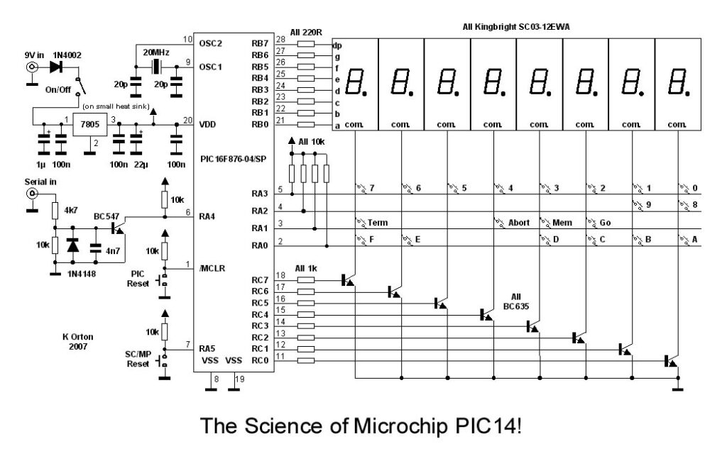
I found a very nice MK14 clone on this page an I intend to build this one. The PIC14 program will run in a PIC16F876, Ports A, B and C providing an interface to the display and keyboard. This is a very neat design and a nice piece of programming, it is a hardware clone of the MK14 using a PIC microcontroller.
This is a page about my SC/MP IDE program which is an editor / emulator / debugger / assembler / disassembler for the SC/MP processor all in one portable Windows executable. When I was 15 years old the Dutch magazine Elektuur published a lot of articles and designs about SC/MP computer boards and as I was fascinated. But I did not have the money to buy these chips and boards, so I build myself a paper version of the SC/MP board with a lot of ones and zeros on little paper. This is how I learned microprocessors and programming. Ten years later I would become a professional software / hardware engineer but mainly on Z80 based boards. Up until a few years ago I forgot about the SC/MP that was my first love but then I build a MK14 board (Karen Orton design) based on a PIC processor and I got interested again. You cannot buy a SC/MP processor anymore for a reasonable price and again I found a solution, I wrote a MK14 emulator for Windows. That gave me another challenge, there was no good assembler available except for a few multiple processor cross assemblers like the SB-assembler. But they all had errors in code generation, strange syntax so every source file had to be rewritten, and most annoying was that the offset (EA) calculation was wrong most of the time. In the sourcecode asm files you would see programmers correcting this by adding or subtracting values but this was not what I wanted. I could not find a decent assembler, so I decided to write my own SC/MP assembler, based in the syntax of the old original assembler. Then I added support for most of the syntax of the other assemblers as well. But in one thing I do not compromise, labels are followed with a colon. As I build IDE’s before for other processors I decided to write a complete development suite for the SC/MP processor, including assembler, disassembler, emulator, MK14,ELBUG and NIBL support, and a single step debugger. It is a portable program in x64 and x32 for Windows, it will run fine under WINE and the exe files are digitally signed with my code certificate. Have fun, Hein Pragt.
To be able to program for the SC/MP (INS8060) you need an assembler but I could not find any good functioning one for Windows 10 / 11. There were still some programs to download but most of them did not work fine or needed extra runtime installed. After some searching I decided that it was time for a new hobby project, building a complete integrated SC/MP (INS8060) development environment. I wrote my own SC/MP (INS8060) assembler in good old portable C code and and re-used the SC/MP emulator that I had wrtitten for the MK14 emuator, and most of the rest I had somewhere in my code library. The result is SC/MP (INS8060) workbench, a portable x64 Windows program that includes an editor, assembler, disassembler, emulator, single step debugger, Intel hex read / write function a terminal window, an MK14 compatible seven segment display with 8 LEDs and keyboard support.
Installation
Download the zip file and unzip it at the place where you want to install it on your hard drive. Then create a shortcut to the program to the desktop and the program is ready for use. It is a so-called portable program which means that it does not use external sources or libraries and does not use the registry. After removing the directory from this program, it has also disappeared completely from your system. The zip file contains the exe files an a example program directory.
First time use
To practice there is an alarmclock_f20.asm file in the example directory, which you can load after which it will be in the shown in the middle edit window. Now you can convert this into machine code by means of the assemble button, this will appear on the left of the screen and be put into the virtual memory of the emulator. The last (or first) .org statement will also be put in the program counter and by simply pressing the run button you can execute the program and follow it on the screen. This will not be very fast because every instruction will perform a screen update of all registers. If you want the program to run faster, you can disable the update of the registry block by means of the update checkbox. The emulator is timing correct, you can adjust the processor speed in the top bar. You can now modify the program, reassemble it and run it again.
The IDE supports four configurations, the SIMPLE one is basically the first simple Electuur design with just 8 leds at 0x100 and keys on 0x200. The MK14 is a fully working MK14 emulator include the type 2 rom. The ELBUG emulation is the second design of Elektuur with a seven segment display and a monitor program. The NIBL implementation is the BASIC computer emulation, including the original rom and a hardware serial I/O emulation. In all configurations you can use the full IDE features including assembler and debugger.
By means of the step button you can execute the program instruction by instruction and check the output and the registers, and with trace on you can see each instruction that is executed. You can also enter the break address for code and ram read/write access. the emulator will then stop at this address and display the registers of that moment. When 0000 is entered in the break fields will be ignored.
You can save the modified code as an asm file again but also save it as a hex file so that you can load the binary code in a circuit or ep(rom) for a real SC/MP circuit. You can also read an Intel-Hex file, which will then be loaded into the internal emulator memory. You can also run tis code when you put the correct start address in the program counter. You can also disassemble this internal emulator memory code after which the source code will appears in the edit screen in the middle. This can then be changed and written back into the emulator memory by means of assemble button.
Memory map
The emulator has the full 64K of ram memory and a part can be protected as rom by setting the Rom-end address. The memory mapped I/O is exactly like the machine hardware that is emulated including the shadow addresses. The keyboard is mapped to the hardware memory address bits of the emulated hardware so I could use original roms without any modifications.
Assembler
The assembler is a typical two pass assembler, on the first pass it does syntax checking and it collects and defines all symbols and during the second pass it will generate the code. The notation of the opcodes is the same as in the SC/MP (INS8060) datasheet, but for PTR register you can either use simply 1 of P1. The assembler contains an expression evaluator that will follow the regular mathematical rules first functions, then * and / and then + and -. The two functions are H() for the high byte of a word value and L() for the low byte of a word value. For compatibility reasons you can also use /label for H() and #label for L(). There are two special symbols that are overloaded, if a operand only contains a * or . this will represent the current address pointer.
The assembler knows the following directives:
.ORG <expression>
Sets the current address pointer to <expression>
.OR
same as .org
.BYTE <expression> [,<expression>]
Defines one or more bytes that will be stored in memory
.DB
Same as .byte
Label: .EQU <expression>
Adds a label with value <expression> to the symbol table
=
Same as .EQU
.BS <expression>
reserves <expression> bytes of memory at current address
.=
Same as .BS
.DS
Same as .BS
.WORD <expression> [,<expression>]
Defines one or more words that will be stored in memory
.DW
Same as .word
.END
defines the end of the source file
.EN
Same as .end
.CR
Dummy ignore
.TF
Dummy ignore
.LF
Dummy ignore
Labels may contain _ A..Z and 0..9 and numbers can be written as: 99 (decimal), 0x99, 0X99, 0H99 or 99H (Hexadecimal)
Version 1.02
This is my second release version 1.02 the code has been heavily tested and debugged by myself and there might still be some little bugs in the program, I am open to bug reports and feature requests.
Download
Here you can download the latest version if this IDE. This download is a zip file containing a portable x64 (and a x32 version) Windows exe programs, and example directory.
This page is dedicated to my fist microprocessor, the INS8060, also called the SC/MP processor. At the time I was 13 years old and did not have much money, I could afford to buy an electronics magazine called Elektuur every month, and they published a simple computer board based on the SC/MP processor. I was very interested in computer technology at that time and I read all I could about the SC/MP processor. The SC/MP is my first processor and nowadays you cannot get the processor anymore (at least not at a reasonable price), but there are emulators in software and hardware that are still available. I have to say that I recemtly bought a SC/MP processor in China for 20 Euros. On this page I will share all documentations, links, schematics and code that I have or have found. INS8060 or SC/MP Processor page
Deze pagina is gewijd aan een MK14 kloon door middel van een PIC processor, de PIC14. Toen ik 13 jaar oud was las ik veel over de INS8060, ook wel de SC/MP-processor genoemd. Ik had niet veel geld en ik kon het me net veroorloven om elke maand een elektronicamagazine genaamd Elektuur te kopen, en ze publiceerden een eenvoudig computerbord gebaseerd op de SC/MP-processor. Ik las alles wat ik kon over de SC/MP-processor. Omdat ik geen geld had om een echte processor te kopen tekende ik de binnenkant van de processor op een groot stuk papier, met het RAM / ROM / toetsenbord en display als registers en ik had veel kleine nul en één papiertjes om de stroom van de bits en bytes in het (papieren) circuit te simuleren. Terugkijkend was dit belachelijk, maar zo heb ik computerontwerpen en binaire logica wel geleerd. Indertijd was er ook een board dat de MK14 heette ook op basis van de SC/MP processor en ik heb destijds overwogen om er een aan te schaffen. Nu ik genoeg geld en tijd heb is de INS8060 processor niet meer koop (althans niet tegen een redelijke prijs). Op deze pagina staat een MK14 emulatie door middel van een PIC processor met de naam PIC14, die qua hardware zich exact gedraagt als een originele MK14. Met een beetje soldeervaardigheid is het in een paar avonden te bouwen. Wanneer u meer wilt weten over de INS8060 ofwel de SC/MP processor kunt u kijken op mijn Engelstalige pagina over deze processor.
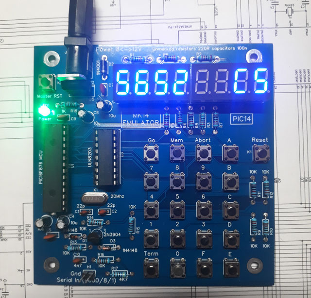
Hier ziet u de versie die ik zelf gemaakt heb, op één print zit de voeding en de processor, op de andere het toetsenbord en het display. Ik heb alles zeer ruim opgezet zodat het eenvoudiger te maken (en debuggen bij een fout) zou zijn. Het geheel is op een houten plaatje gemonteerd zodat het in de showkast kan staan en voor gebruik stabiel staat.
Een kennis uit de UK stuurde me een PCB voor een PIC14 kloon die gebruikt maakt van een UN2003 transistor array IC en een fijne compacte opstelling heeft. Ook deze is gebaseerd op het originele ontwerp van Karen. Ik had alle onderdelen op voorraad dus op een druilerige zaterdagavond was het in een paar uurtjes in elkaar gezet.
Nog een PIC14
En nog een PIC14
Wanneer u zelf een PIC14 wilt bouwen en niet wilt bedraden op experimenteerboard, is het lastig om nog een PCB te vinden. Het Nederlandse bedrijf Budgetronics.eu levert een compleet bouwpakket dat ook gebaseerd is op het ontwerp van Karen tegen een schappelijke prijs.
Dit is de originele versie van de MK14 single board computer, het was geen Acorn-product maar een eerste stap in de creatie van Acorn Computers. Chris Curry werkte met Clive Sinclair aan de ontwikkeling van de MK14 als een product van Science of Cambridge / Sinclair. De MK14 is gemaakt door Science of Cambridge (later Sinclair Computers en tenslotte Sinclair Research). De MK14 was het gebaseerd op de National Semiconductors SC/MP (INS8060) processor en werd het als bouwpakket verkocht. Het kon geprogrammeerd worden voor middel van een ingebouwd monitor programma en het hexadecimale toetsenbord en de zevensegment displays.
The shipment method for all of Europe is PostNL mailbox packages with track & trace. Shipping costs within the Netherlands are Euro 4.90, other countries have shipping costs depending on the location. These shipping costs will always be clearly stated. Shipping is usually done the same day or the next working day from the Netherlands. All components are shipped as safely as possible, when necessary in anistatic foam.


.jpg)
.jpg)