| INS1671 | Asynchronous/synchronous transmitter/receiver (National Semiconductor) Replacement for FD1671 |
| INS1771-1 | Floppy disk formatter/controller (National Semiconductor) Replacement for FD1771-1 |
| SAB1791 | Floppy disk formatter/controller SS/DD (Siemens) |
| SAB1793 | Floppy disk formatter/controller SS/DD (Siemens) |
| SAB1795 | Floppy disk formatter/controller SS/DD (Siemens) |
| SAB1797 | Floppy disk formatter/controller SS/DD (Siemens) |
| SAB2793B | Advanced floppy disk formatter/controller (Siemens) |
| SAB2797B | Advanced floppy disk formatter/controller (Siemens) |
| 7201A | Multi-protocol serial communication controller (Siemens) |
| UPD7210 | Intelligent general purpose interface bus controller (NEC) |
| 8202A | Dynamic RAM controller (Intel) |
| INS8202 | Tri-state 8-bit bus driver (National Semiconductor) |
| 8203 | Dynamic RAM controller (2164, 2117 and 2118 dram) (Intel) |
| INS8203 | Tri-state 8-bit bus driver (inverting) (National Semiconductor) |
| INS8208 | 8-bit bidirectional bus driver (National Semiconductor) |
| INS8212 | 8-bit I/O port (National Semiconductor) |
| 8216 | 4-bit bidirectional bus driver. (NEC, National Semiconductor) |
| 8224 | Clock generator and driver (Intel, National Semiconductor) |
| 8226 | 4-bit bidirectional bus driver (inverting). (NEC, National Semiconductor) |
| 8228 | System controller and bus driver (Intel, National Semiconductor) |
| 8237A | High performance programmable 4-channel DMA controller (AMD, Intel, NEC, Siemens, UMC) |
| 8238 | System controller and bus driver (Intel, National Semiconductor) |
| 8250 | Programmable asynchronous communications element (National Semiconductor, UMC) |
| 8251A | Programmable communication interface (AMD, Intel, NEC) |
| 8253 | Programmable interval timer (AMD, Intel, NEC, National Semiconductor, UMC) |
| INS8254 | 2 8-bit programmable I/O ports. (National Semiconductor) |
| 8255A | Programmable peripheral interface (AMD, Intel, NEC) |
| 82C55A | CHMOS programmable peripheral interface. (AMD, Intel, OKI, UMC) |
| INS8255 | Programmable peripheral interface (National Semiconductor) |
| 8257 | Programmable 4-channel DMA controller (Intel, NEC, National Semiconductor) |
| 8259A | Programmable interrupt controller (AMD, Intel, NEC, Siemens, UMC) |
| 82C59A | CHMOS programmable interrupt controller (AMD, Intel, OKI) |
| INS8259 | Programmable interrupt controller (National Semiconductor) |
| 8282 | Octal latch with 3-state outputs (Intel, NEC) |
| 8283 | 8-bit latch with 3-state outputs (Intel, NEC) |
| 8286 | 8-bit bus transeiver with 3-state outputs (Intel, NEC) |
| 8287 | 8-bit bus transeiver with 3-state outputs (Intel, NEC) |
| 8291A | GPIB talker/listener (Intel) |
| 8294A | Data encryption/decryption unit (Intel) |
| DP8350 | Programmable CRT controller (National Semiconductor) |
Category: Eng
English
82xx support and peripheral chips
| 82C01 | Capacitance keyboard encoder(UMC) |
| 8202A | Dynamic RAM controller (Intel) |
| INS8202 | Tri-state 8-bit bus driver(National Semiconductor) |
| 8203 | Dynamic RAM controller(Intel) |
| 8205 | High-speed 1 out of 8 binary decoder (Intel) |
| 8206 | Error detection and correction unit (Intel) |
| 8207 | Dual-port dynamic RAM controller (Intel) |
| 8208 | Dynamic RAM controller (Intel) |
| INS8208 | 8-bit bidirectional bus driver(National Semiconductor) |
| 82C12 | 8-bit I/O port(OKI) |
| INS8212 | 8-bit I/O port (National Semiconductor) |
| 8216 | 4-bit bidirectional bus driver. (National Semiconductor) |
| 8224 | Clock generator and driver (National Semiconductor) |
| 8226 | 4-bit bidirectional bus driver. (NEC, National Semiconductor) |
| 8228 | System controller and bus driver ( Intel, National Semiconductor) |
| 8237A | High perf. 4-channel DMA controller (AMD, Intel, NEC, Siemens, UMC) |
| 8238 | System controller and bus driver (Intel, National Semiconductor) |
| 8243 | Input/Output expander(Intel, NEC) |
| 8250 | Programmable async comm, element (National Semiconductor, UMC) |
| 8251 | Programmable communication interface (AMD, National Semiconductor) |
| INS8254 | 2 8-bit programmable I/O ports. (National Semiconductor) |
| 8255A | Programmable peripheral interface(AMD, Intel, NEC) |
| INS8255 | Programmable peripheral interface (National Semiconductor) |
| SAB8256A | Programmable multifunction UART (Siemens) |
| 8257 | Programmable 4-channel DMA controller (Intel, NEC, National Semiconductor) |
| 8259A | Programmable interrupt controller (AMD, Intel, NEC, Siemens, UMC) |
| 8272A | Single/double density floppy disk controller (Intel, UMC) |
| 8273 | Programmable HLDC/SLDC protocol controller (Intel) |
| 8274 | Multi-protocol serial controller (Intel) |
| 8275H | Programmable CRT controller (Intel) |
| 8276H | Small system CRT controller(Intel) |
| 8279 | Programmable keyboard/display interface (Intel, NEC) |
| 8282 | Octal latch with 3-state outputs (Intel, NEC) |
| 8283 | 8-bit latch with 3-state outputs (Intel, NEC) |
| 8284A | Clock generator and driver (Intel, NEC) |
| 8286 | 8-bit bus transeiver with 3-state outputs (Intel, NEC) |
| 8287 | 8-bit bus transeiver with 3-state outputs (Intel, NEC) |
| 8288 | Bus controller (Intel, NEC) |
| 8289 | Bus arbiter (Intel, NEC) |
| 8291A | GPIB talker/listener(Intel) |
| 8292 | GPIB controller (Intel) |
| 8294A | Data encryption/decryption unit (Intel) |
| INS8298 | LLL BASIC interpreter for 8080A CPU (National Semiconductor) |
| 82062 | Winchester disk controller(Intel) |
| 82064 | Winchester disk controller (Intel) |
| 82077SL | Floppy disk controller (Intel) |
| 82078 | Floppy disk controller (Intel) |
| 82091AA | Advanced integrated peripheral (Intel) |
| 82188 | Integrated bus controller (Intel) |
| 82258 | Advanced 16-bit 4-channel DMA controller (Intel) |
| 82284 | Clock generator and ready interface (AMD, Intel) |
| 82C284 | CHMOS clock generator and ready interface (Intel, UMC) |
| 82288 | Bus controller (Intel) |
| 82289 | Bus arbiter (Intel) |
| 82370 | Integrated system peripheral(Intel) |
| 82380 | 32-bit DMA controller (Intel) |
| 82384 | Clock generator and reset interface (Intel) |
| 82450 | Programmable async. Comm. Element (UMC) |
| 82501 | Ethernet serial interface (Intel) |
| 82C502 | Ethernet transceiver chip (Intel) |
| 82503 | Dual serial transceiver (Intel) |
| 82530 | Serial communications controller (Intel) |
| 82586 | LAN coprocessor (Intel) |
| 82588 | LAN controller (Intel) |
| 82593 | CSMA/CD core LAN controller (Intel) |
| 82595 | ISA/PCMCIA high-integration ethernet controller (Intel) |
| 82720 | Graphics display controller (Intel) |
| 82730 | Text coprocessor (Intel) |
| 82731 | Video interface controller(Intel) |
| 82C6818 | Real time clock and RAM (UMC) |
IC Manufacturer Codes
IC Manufacturer Codes Reference Table
Integrated Circuit (IC) manufacturer codes are unique identifiers printed on chips to indicate their origin and production details. These alphanumeric markings differ among companies, but all serve the same purpose – to ensure clear traceability and authenticity. Identifying the maker of an IC begins with reading its prefix, the abbreviation printed on the chip. This prefix links to a registered company — for instance, SN or TL typically represents Texas Instruments, LM may belong to National Semiconductor or TI, and MC points to Motorola or ON Semiconductor. Sometimes I have the same chip from different manufacturer f.i. SN and DM the chips are compatible.
| Abbreviation | Manufacturer | Abbreviation | Manufacturer |
| AM | Advanced Micro Devices (AMD) | A | National Semiconductor |
| AMSREF | Advanced Monolithic Systems | ADC | National Semiconductor |
| OM | AEG | CLC | National Semiconductor |
| PCD | AEG | COP | National Semiconductor |
| PCF | AEG | DAC | National Semiconductor |
| SAA | AEG | DM | National Semiconductor |
| SAB | AEG | DP | National Semiconductor |
| SAF | AEG | DS | National Semiconductor |
| SCB | AEG | F | National Semiconductor |
| SCN | AEG | L | National Semiconductor |
| TAA | AEG | LF | National Semiconductor |
| TBA | AEG | LFT | National Semiconductor |
| TCA | AEG | LH | National Semiconductor |
| TEA | AEG | LM | National Semiconductor |
| A | Allegro Microsystems | LMC | National Semiconductor |
| STR | Allegro Microsystems | LMD | National Semiconductor |
| UCN | Allegro Microsystems | LMF | National Semiconductor |
| UDN | Allegro Microsystems | LMX | National Semiconductor |
| UDS | Allegro Microsystems | LPC | National Semiconductor |
| UGN | Allegro Microsystems | MF | National Semiconductor |
| EP | Altera | MM | National Semiconductor |
| EPM | Altera | NH | National Semiconductor |
| PL | Altera | UNX | National Semiconductor |
| A | AMD | PB | NEC |
| Am | AMD | PC | NEC |
| AMPAL | AMD | PD | NEC |
| PAL | AMD | UPD | NEC |
| OM | Amperex | UPD8 | NEC |
| PCD | Amperex | NJM | New Japan Radio Corp. |
| PCF | Amperex | NSC | Newport |
| SAA | Amperex | SM | Nippon Precision Circuits |
| SAB | Amperex | NC | Nitron |
| SAF | Amperex | MM | Oki |
| SCB | Amperex | MSM | Oki |
| SCN | Amperex | MC | ON Semiconductor |
| TAA | Amperex | EF | ON Semiconductor (previously Thomson) |
| TBA | Amperex | ET | ON Semiconductor (previously Thomson) |
| TCA | Amperex | GSD | ON Semiconductor (previously Thomson) |
| TEA | Amperex | HCF | ON Semiconductor (previously Thomson) |
| V | Amtel | L | ON Semiconductor (previously Thomson) |
| AD | Analog Devices | LM | ON Semiconductor (previously Thomson) |
| ADEL | Analog Devices | LS | ON Semiconductor (previously Thomson) |
| ADG | Analog Devices | M | ON Semiconductor (previously Thomson) |
| ADLH | Analog Devices | MC | ON Semiconductor (previously Thomson) |
| ADM | Analog Devices | NE | Philips |
| ADP | Analog Devices | LM | Texas Instruments |
| CA | RCA | SN | Texas Instruments |
| CD | RCA | TL | Texas Instruments |
| HEP | RCA | UA | Fairchild Semiconductor |
| LM | National Semiconductor / TI | LF | Texas Instruments |
| MC | Motorola (ON Semiconductor) | LMV | Texas Instruments |
| NE | Philips | UC | Unitrode |
| NTE | NTE Electronics | LT | Linear Technology |
| MAX | Maxim Integrated | LTC | Linear Technology |
| ADI | Analog Devices | ST | STMicroelectronics |
| SG | Silicon General | STR | Sanken |
| TDA | Philips / STMicroelectronics | STRM | Sanken |
| TL | Texas Instruments | KA | Samsung |
| LMH | Texas Instruments | LA | Sanyo |
| MC | Motorola / ON Semiconductor | TA | Toshiba |
| NJU | New Japan Radio (JRC) | TC | Toshiba |
| HA | Hitachi | AN | Panasonic |
| HD | Hitachi | MN | Panasonic |
| BA | Rohm Semiconductor | BA | Rohm Semiconductor |
| BD | Rohm Semiconductor | CXA | Sony |
| CXA | Sony | CXD | Sony |
| CXD | Sony | IR | International Rectifier |
| IRF | International Rectifier | IX | IXYS Semiconductor |
| FDS | Fairchild Semiconductor | MMBT | Diodes Inc. |
| LMK | Texas Instruments | XC | Xilinx |
| XC | Xilinx | DS | Dallas Semiconductor |
| DS | Dallas Semiconductor | ISL | Intersil |
| ISL | Intersil | HN | Hitachi |
| KIA | KEC | SM | Silicon Motion |
| SI | Siliconix (Vishay) | VN | STMicroelectronics |
| TLV | Texas Instruments | MAX | Maxim Integrated |
| UC | Unitrode (now TI) | NJM | New Japan Radio Corp. |
| MCP | Microchip Technology | PIC | Microchip Technology |
| AT | Atmel (now Microchip) | SST | Silicon Storage Tech. |
| XC | Xilinx | EP | Altera |
| EPF | Altera | EPM | Altera |
MK14 component list

This is the original component list of the MK14 processor board.

IC’s
MK14 Board component list
IC1, IC2 DM74S571
IC3 DM74S571
CPU 1SP-8A/600(8060)
IC4 MM2111-1N 256 x 4 RAM
IC5 MM2111-1N 256 × 4 RAM
IC6 MM2111-1N 256 x 4 RAM
IC7 MM2111-1N 256 x 4 RAM
IC8 INS8154N
IC9 DM74LS157
IC10 DM74LS157
IC11 DM80L95
IC12 DM74LS173
IC13 DM7445
IC14 DM7408
IC15 Dm7408
IC16 DM74LS08
IC17 DM74LS00
IC18 DM74LS04
IC19 LM340
Crystal 4.433619 MH2
Intel MSC-48 chips

The MCS-48 microcontroller series was the first range of microcontroller from Intel and it was originally released in 1976. The first chips were the 8048, 8035 and 8748 and the 8048 is probably the most used chip of this family. The first chips were produced using NMOS and in the early 1980s they became available in CMOS. The chips were produced until the 1990tie but there are still a lot around these days.
The MCS-48 microcontroller series has a modified Harvard architecture, with internal or external program ROM and 64 to 256 bytes of internal (on-chip) RAM. The I/O is mapped into its own address space, separate from programs and data and that made it a perfect controller in f.i. keyboards and toys. The original IBM PC keyboard used an 8048 as its internal microcontroller.
Common chips that are still available today are:
| Device | Internal | Memory | Remarks |
| 8035 | none | 64 × 8 RAM | |
| 8038 | none | 64 × 8 RAM | |
| 8039 | none | 128 × 8 RAM | |
| 8040 | none | 256 × 8 RAM | |
| 8048 | 1K × 8 ROM | 64 × 8 RAM | 27× I/O ports |
| 8049 | 2K × 8 ROM | 128 × 8 RAM | 27× I/O ports |
| 8050 | 4K x 8 ROM | 256 × 8 RAM | |
| 8748 | 1K × 8 EPROM | 64 × 8 RAM | 4K program memory expandable, 2× 8-bit timers, 27× I/O ports |
| 8749 | 2K × 8 EPROM | 128 × 8 RAM | 2× 8-bit timers, 27× I/O ports |
Simple processor
The 8048 is a very simple (but powerful) processor, with only one A4 page of instructions. You can use the internal ROM and have a lot of I/O pins, but whem activating the EA pin, you can also map the ROM to outside and use a eeprom or eprom to hold the code.
Pinout 8048 microcontroller

Internal diagram of the 8048

Schematic 8048 with external Eprom

Intel_8048_Single_Board_Computer on GitHub
https://github.com/jim11662418/Intel_8048_Single_Board_Computer
A simple Intel 8048 Single Board Computer. The firmware was assembled with the Macro Assembler AS with full schematics and sourcecode of the project, even the sourcecode of a monitor programm. It is fun to play with such aq simple, but yet powerful, micrcontroller. There is a good open source assembler:
http://john.ccac.rwth-aachen.de:8000/as/
Documentation and downloads
Guitar tone capacitors
When it comes to guitar tone, capacitor value is what matters most. Capacitors also feature a voltage rating that also determines the physical size of the cap but because almost all capacitors can easily handle the voltages produced by your guitar, the voltage ratings is not so important. The value of the capacitor will roll your guitar’s tone back and the higher the value, the darker the tone and the lower the value, the brighter the tone. While there is a wide range of values to choose from, most electric guitars feature only a few options.
Popular values
- .015 µF (is equal to 15 nF)
- .022 µF (is equal to 22 nF)
- .047 µF (is equal to 47 nF)
15 nF
15 nF capacitors are not as popular as the other two but they are perfect for fine control of your high-end frequencies throughout the full sweep of your tone knob. They are also fantastic for taming harsh frequencies in your signal.
22 nF
22 nF is the most common value and however they interact differently with humbucking and single-coil pickups, they work great on both. But they are most often found in humbucker-equipped guitars. They are know for a warm and woolly sound.
47 nF
.047 µF capacitors are also a popular choice, they are darker than the other two capacitor values. This is why Fender often uses them for their brighter Stratocaster and Telecaster pickups. Turning the know you will hear that the high-end detail will disappear very fast. The dark, mid-range sound is especially popular with jazz players.
Type of capacitor
You can use the cheap Ceramic capacitors, but most people do not like them for guitars, because they are rather inacurate. The old Paper-in-oil capacitors are considered the best, but they are very hard to find and very expensive. So the best and most used capacitor is the Polypropylene capacitor, mostly recognisable by its red or orange color.

Swapping your tone capacitors is a powerful, affordable and easy-to-accomplish modification.
Kind regards, Hein Pragt.
Types of packages
Components come in several packages and it is not always so clear what package type you will need. I sell mosly DIP / DIL packages beacuse they are often used in old electronic designs and computers, but I also sell more modern packages. Analog chips and transistors also come in different packages. On this page I have soms pictures of the different package types.


Intel MCS-48 processor family

One of the forgotten microprocessors / microcontrollers is the Intel MCS-48 family which was Intel’s first microcontroller and was released in 1976 and was manufactured into the 1990ties. At the bottom of this page I have a overview of the many members of this microcontroller family. The 8048 is the most prominent member of the family. The MCS-48 family has a modified Harvard architecture, with internal or external program ROM and 64 to 256 bytes of internal RAM. The I/O is mapped into its own address space, separate from programs and data. Because of its low costs and single chip operation its was used in many cost-sensitive consumer electronics devices such as TV remotes, computer keyboards (TRS-80 Model II, IBM PC), and toys. Years later the MCS-48 chips were replaced by the very successful MCS-51 series that is still manufactured (and used) today.
I also have a Facebook Group on Retro Computing and Electronics, feel free to join!
The MCS-48 processor family
NEC UPD8022C (Processor)
 In 1976 Intel and NEC agreed that NEC could make second source chips from Intel and NEC also made and 8022 from Intel. The 8022 is as standard
MCS-48 series chip and has a modified Harvard architecture, with 2K × 8 ROM 64 × 8 RAM + A/D-converter. I cannot find any datasheet on this chip.
In 1976 Intel and NEC agreed that NEC could make second source chips from Intel and NEC also made and 8022 from Intel. The 8022 is as standard
MCS-48 series chip and has a modified Harvard architecture, with 2K × 8 ROM 64 × 8 RAM + A/D-converter. I cannot find any datasheet on this chip.
wikipedia MCS-48 / 8035 (Processor) (Eng)
Intel 8035 (Processor)
 In 1976 Intel introduced the MCS-48 microcontroller series, its first members were 8048, 8035 and 8748. In the beginning these chips were using NMOS
technology, later they became available in CMOS technology. The MCS-48 series has a modified Harvard architecture, with internal or external program
ROM and 64–256 bytes of internal (on-chip) RAM. The I/O is mapped into its own address space, separate from programs and data.The MCS-48 series was
later replaced by the very successful MCS-51 series but the chips are still used in cheap consumer electronics devices such as TV remotes, computer
keyboards. and toys. Compared to the standard 8048 the 8035 has no internal ROM and 64 x 8 bytes internal RAM memory.
In 1976 Intel introduced the MCS-48 microcontroller series, its first members were 8048, 8035 and 8748. In the beginning these chips were using NMOS
technology, later they became available in CMOS technology. The MCS-48 series has a modified Harvard architecture, with internal or external program
ROM and 64–256 bytes of internal (on-chip) RAM. The I/O is mapped into its own address space, separate from programs and data.The MCS-48 series was
later replaced by the very successful MCS-51 series but the chips are still used in cheap consumer electronics devices such as TV remotes, computer
keyboards. and toys. Compared to the standard 8048 the 8035 has no internal ROM and 64 x 8 bytes internal RAM memory.
wikipedia MCS-48 / 8035 (Processor) (Eng)
UPD80C35 Processor Datasheet
Intel 8039 (Processor)
 The 8039 is also a member of the MCS-48 processor family. Compared to the standard 8048 the 8039 equals to a 8035 and has no internal ROM and
128 x 8 bytes internal RAM memory on chip.
The 8039 is also a member of the MCS-48 processor family. Compared to the standard 8048 the 8039 equals to a 8035 and has no internal ROM and
128 x 8 bytes internal RAM memory on chip.
wikipedia MCS-48 / 8035 (Processor) (Eng)
P8039AHL Processor Datasheet
>
Intel 8039 (Processor)
The 8040 is also a member of the MCS-48 processor family. Compared to the standard 8048 the 8040 equals to a 8035 and has no internal ROM and
256 x 8 bytes internal RAM memory on chip.
wikipedia MCS-48 / 8035 (Processor) (Eng)
P8039AHL Processor Datasheet
8041 (UPI)
 The 8041 is also a member of the MCS-48 processor family and it use is a Universal Peripheral Interface 8 bit Slave Microcontroller. It has
1024 x 8 ROM and 64 x 8 RAM on chip. The 8041 is essentially a ‘‘slave’’ microcontroller, or a microcontroller with a slave interface included
on the chip. Interface registers are included to enable the UPI device to function as a slave peripheral controller in the MCS Modules and iAPX
family, as well as other 8-, 16-, and 32-bit systems.
The 8041 is also a member of the MCS-48 processor family and it use is a Universal Peripheral Interface 8 bit Slave Microcontroller. It has
1024 x 8 ROM and 64 x 8 RAM on chip. The 8041 is essentially a ‘‘slave’’ microcontroller, or a microcontroller with a slave interface included
on the chip. Interface registers are included to enable the UPI device to function as a slave peripheral controller in the MCS Modules and iAPX
family, as well as other 8-, 16-, and 32-bit systems.
wikipedia 8048 (Eng)
UPD8041 DatasManual
D8741 (UPI)
 The 8741 is also a member of the MCS-48 processor family and it use is a Universal Peripheral Interface 8 bit Slave Microcontroller. It has
1024 x 8 EPROM and 64 x 8 RAM on chip. The 8741 is essentially a ‘‘slave’’ microcontroller, or a microcontroller with a slave interface included
on the chip. Interface registers are included to enable the UPI device to function as a slave peripheral controller in the MCS Modules and iAPX
family, as well as other 8-, 16-, and 32-bit systems.
I have four D8741 from NEC and two D8741 from Intel in my collection.
The 8741 is also a member of the MCS-48 processor family and it use is a Universal Peripheral Interface 8 bit Slave Microcontroller. It has
1024 x 8 EPROM and 64 x 8 RAM on chip. The 8741 is essentially a ‘‘slave’’ microcontroller, or a microcontroller with a slave interface included
on the chip. Interface registers are included to enable the UPI device to function as a slave peripheral controller in the MCS Modules and iAPX
family, as well as other 8-, 16-, and 32-bit systems.
I have four D8741 from NEC and two D8741 from Intel in my collection.
wikipedia 8048 (Eng)
D8741 DatasManual
8042 (UPI)
 The 8042 is also a member of the MCS-48 processor family and it use is a Universal Peripheral Interface 8 bit Slave Microcontroller. It has
4096 x 8 ROM and 256 x 8 RAM on chip. The 8042 is essentially a ‘‘slave’’ microcontroller, or a microcontroller with a slave interface included
on the chip. Interface registers are included to enable the UPI device to function as a slave peripheral controller in the MCS Modules and iAPX
family, as well as other 8-, 16-, and 32-bit systems.
The 8042 is also a member of the MCS-48 processor family and it use is a Universal Peripheral Interface 8 bit Slave Microcontroller. It has
4096 x 8 ROM and 256 x 8 RAM on chip. The 8042 is essentially a ‘‘slave’’ microcontroller, or a microcontroller with a slave interface included
on the chip. Interface registers are included to enable the UPI device to function as a slave peripheral controller in the MCS Modules and iAPX
family, as well as other 8-, 16-, and 32-bit systems.
wikipedia 8048 (Eng)
MBL8042 DatasManual
8048 (MCU)
The 8048 is also a member of the MCS-48 processor family. The 8048 has 1Kb x 8 bytes ROM and 64 x 8 bytes
internal RAM memory on chip, and 27 I/O lines.
I have two PE8048 from Intel and four MAB8048 from Philips in my collection.
wikipedia 8048 (Eng)
8048 DatasManual
P8748 (MCU)
 The 8748 is also a member of the MCS-48 processor family. Compared to the standard 8048 the 8748 has 1Kb x 8 bytes PROM and 64 x 8 bytes
internal RAM memory on chip, and 27 I/O lines.
The 8748 is also a member of the MCS-48 processor family. Compared to the standard 8048 the 8748 has 1Kb x 8 bytes PROM and 64 x 8 bytes
internal RAM memory on chip, and 27 I/O lines.
wikipedia 8048 (Eng)
P8748 DatasManual
8049 (MCU)
The 8049 is also a member of the MCS-48 processor family. Compared to the standard 8048 the 8049 has 2Kb x 8 bytes ROM and 128 x 8 bytes
internal RAM memory on chip.
wikipedia 8048 (Eng)
MBL8042 DatasManual
8050 (8 bit Microsontroller)
 The 8050 is also a member of the MCS-48 processor family. Compared to the standard 8048 the 8039 has 4K x 8 ROM and 256 × 8 RAM memory on chip.
M5M8050H Datasheet (pdf)
The MSC-48 internals

The MSC-48 pin layouts

MSC-48 programming / technical reference
Book 8088 laptop

My first IBM compatible development machine was a IBM-XT clone with a 8088 processor, 640 MB memory, a CGA graphics card and a 10 Mb hard disk and two floppy drives. I later changed the 8088 for a NEC V20 and added a bigger hard disk. I was running DOS and the first releases of MS Windows up to version 3.0, I have some good memories from that time, beside development I also used the machine for games and I remember many hours of fun. But very soon I got an Intel 286 AT machine and then a Intel 286 and so on. At that time I was programming in C and 8086 assembler and I still have some code I wrote at that time.
Nowadays there are not that many 8088 / 8086 machine left and the prices of old retro IBM-PC machines is still rising. Also there are not that many 8088 DIY projects, it looks like a not so popular processor. I have been looking for a 8088 / 8086 system for a long time and beside some expensive development boards there is not that much on the market. Then I found this Book 8088 laptop on a Chinese website and at first it looked a little too good to ben true. A complete laptop with LCD screen, a VGA compatible video card, am OPL compatible soundcard, SD drive with preinstalled DOS 6 and Windows 3.0 and some nice software, and all that around 200 euros.
I ordered one and was surprised by this little device, it worked out of the box and after a good charge I tested most of the features. It is nice to see a dos machine boot and it brings back good memories. The speed is also “compatible” and that is a strange experience, but it is accurate. The machine has a NEC V20 processor on board and there is room for a 8087 co-processor.

It has 640 KB of ram, a parallel and serial port on the back, a USB host plug for USB sticks (that mound as drive D) to transfer data and files, it has an ISA header on the back where you can add a standard 3 slot ISA bus and it has a build in battery.

I also played some of my old games on this machine and it feels exactly like the old days, I am planning to look for more of my favorite games.

There are some plans I have, I want to build a 8088 / 8086 IDE with a build in IBM-PC emulator, I can use this machine as a reference. I am looking for a serial mouse, that would be nice using Windows 3.0. A also ordered the ISA extension card and a ISA serial card. I also intend to change the BIOS rom because there is an alternative that is open source and GPL and I want to see if the machine runs on a standard intel 8088 processor. A lot of things to do, and hopefully a lot of fun.
Regards, Hein Pragt
Retroshield INS8060

The INS8060 or SC/MP processor was my first “love” when I was 15 years old. But at that time the processor and boards were far too expensive for me. It was in my 60ties when I really went into Retro computing that I managed to buy an original (white ceramic) SC/MP chip and later I bought a INS8060, the second version that did not need the negative voltage. I kept the processors in a box, but it is always nice to have them running again, but I could not bring myself to re-building an old SC/MP project. I very rarely get a SC/MP INS8060 processor for my webshop, but if I find one I will put it in the shop!
RetroShield
I have a lot of so called RetroShield boards for the Arduino Mega board, this is a way to connect an old processor to the Arduino Mega andlet the Arduino Mega run as ROM / RAM and I/O. I found there was also a RetroShield for the INS8060 so I ordered one. After som soldering it worked as usual I rewrote the code and it runs NIBL basic for the SC/MP processor using the (very slow) serial capabilities of the IND8060 processor.

But it works and it is nice to see the old processor running. It has no practical use, but it is better than keeping the processor hidden in a box. At the bottom of the page I have a download link for the code I run in the Arduino Mega.
Download and links
My Arduino Mega sourcecode:
I did write a complet page about the SC/MP (INS8060) processor with a lot of documentation:
https://www.heinpragt-software.com/ins8060-or-scmp-processor/
And also I wrote a development IDE for the SC/MP (INS8060) processor, including an emulator, an assembler / disassembler.
https://www.heinpragt-software.com/sc-mp-processor-ide/
Have fun!
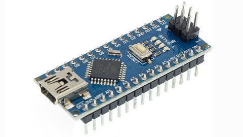
Arduino boards / AVR chips

I also sell Arduino boards like the Arduino Nano, Arduino Uno and several AVR based chips in mu webshop and although they are strictly not retro, they are used in a lot of Retro replicas, retroshields and chip testers. I build a lot of chip testers based on an Arduino board and I also have some PCB’s for these in my webshop. On this page I will tell you a little more about these AVR chips. AVR is a family of microcontrollers developed since 1996 by Atmel and acquired by Microchip Technology in 2016. The AVR chips are modified Harvard architecture 8-bit RISC single-chip microcontrollers and they were one of the first microcontroller families to use on-chip flash memory for program storage.
The AVR architecture was conceived by two students at the Norwegian Institute of Technology (NTH) named Alf-Egil Bogen and Vegard Wollan. Atmel says that the name AVR is not an acronym but it is commonly accepted that AVR stands for Alf and Vegard’s RISC processor. One of the first chips of the AVR line was the AT90S8515 and the processors got a big boost when the Arduino platform was released in 2005 and featured the ATmega8 AVR microcontrollers.
The Arduino based boards (but also the individual chips using SPI) can be easily programmed in assembler and the ‘C’ and ‘C++’ language and there are a lot of ready to use libraries for different devices and communication protocols.. The fact that (most of ) these chips use 5V power supply makes them also interesting to use in combination with old hardware and old chips. They are often used as a boot device and serial controller in several designs like the Z80 MBC and the Apple1 replica.
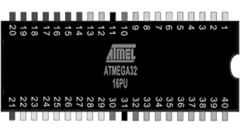
The ATMega32 is a high-performance, low-power Microchip 8-bit AVR® RISC-based microcontroller that combines 32 KB ISP flash memory with 1 KB EEPROM, 2 KB SRAM, 54/69 general purpose I/O lines, 32 general purpose working registers, three flexible timer/counters with compare modes, internal and external interrupts, serial programmable USART, an 8-channel 10-bit A/D converter, programmable watchdog timer with internal oscillator, SPI serial port, and five software selectable power saving modes. The device operates between 1.8-5.5 volts. This makes it suitable as external rom for boot and serial and I/O device for retro microprocessors like the Z80. The ATMega32 is used in a lot of MBC (Minimal Computer Board) designs like the Z80 MBC.

The Arduino Mega is a big Arduino board based on the ATmega2560. It has 256 KB of Flash Memory ( 8 KB used by bootloader), 8 KB Sram and 4 KB Eeprom, 54 digital input/output pins, 16 analog inputs, 4 UARTs (hardware serial ports) and a 16 MHz crystal oscillator. This makes it perfect to emulate Rom / Ram and I/O for a lot of old 8bit microprocessors. There are a lot of so called Retroshields for a wide verity of 8 bit processors like the Z80, the 6502, the 1802, the 2605 and 68xx processors. Sometimes even a small system using basic or emulation of an old computer is available in open source.
The Ardiono Uno and the Arduino Nano are often used as basic boards for chip testers, ISP programmers and f.i. as serial interface on a Retro computer where these boards replace a lot of glue logic. On the Apple1 replica the Arduino Nano replaces the terminal interface emulating the keyboard and the CRT interface. I also sell a dram tester based on Arduino Uno or Arduino Nano boards.

In retro designs the AVR chips are very handy to replace a lot of glue logic and I/O devices, because the AVR chips and boards support SPI they can easily interface to cheap SD card disk drives and realtime clock boards. So even if these chips are not retro themselves, the are often used in combination with Retro computers.
Have fun, regards, Hein Pragt.
Atmega328 retro board

Sometimes you have a project that you started and did not finish that keeps staring you in the eye every time you enter your shack. This was one of mine, I was planning to build a copy of the famous MPF1 board, but after soldering the keys and the displays, it stopped. After a while the urge of building a copy of the MPF1 faded and the board was laying on my desk. Then I thought about creating an ATMega328 based universal retro board that I could use to emulate f.i. a KIM1 or even a MPF1. The problem was the amount of I/O pins an ATMega328 has when using an external oscillator. But with some deep thinking and some clever design I managed to fit it all on one ATMega328 and keeping the RX/TX pins free for serial communication for debugging messages. This is the design I came up with.

I use two common cathode seven segment X 4 displays and I driver them using an ULN2803 that contains 8 Darlington transistor circuits. The outputs drive the displays (active to ground) but also the scanlines of the keyboard. As I wanted nine rows (MPF1) I had to use a clever trick, there is a 9e state and that is “all off”. By connecting the last row to the ground I can read these pins if all scanlines are inactive. The last button is hardwired to the reset pin. Furthermore the design is very straightforward, the TX line is used as an output for a scanline so it can be used as serial out at the same time. Only the first display will light up a little extra. The RX pin is left free so this can also be used.
The design is made in a way that the ATMega328 chip can be easily replaced with an Arduino Uno, that makes development very easy as you can download the sketch from the IDE and monitor using the terminal of the IDE. When all is working fine, just program the code in an ATMega328 and put the chip in place. Here I have a zip file with the basic test code to see if the hardware is working and an example of the keyboard and display drivers code.

When everything was working I took the sourcecode of the KIMUNO project and cleaned up the code and added my own keyboard and display drivers. This took me a while because the code was a little unclear sometimes. I reformatted / restuctured the code, deleted some unused code and added comment. After a few evening the KIM1 clone was working on my hardware. At the end of the page I included my full sourcecode of the project. And after putting the code inside a standalone ATMega328, this was the result. A working KIM1 emulator.

I hope I have inspired someone to build this and even add more features or other emulations. I still want to write a full MPF1 emulation for this board, but that is one of the future plans.
Sourecode KIM1 ATMega328
Have fun, regards, Hein Pragt.
Arduino Uno ATMega328 pins
The Arduino Uno is not a very Retro style board but it is one of the boards that made microcontrollers available for the main public with a simple and free IDE and opensource hardware. I like using the AVR chips and nowadays a lot new designs of old retro computers contain an AVR chip to replace al lot of glue logic chips. There are even complete emulations of old system available on AVR chips and f.i. de KIM-Uno is a complete emulation of the very old KIM computer board on an Arduino Uno.
AVR is a family of microcontrollers developed since 1996 by Atmel and these are modified Harvard architecture 8-bit RISC single-chip microcontrollers. AVR was one of the first microcontroller families to use on-chip flash memory for program storage. The AVR architecture was conceived by two students at the Norwegian Institute of Technology (NTH) Alf-Egil Bogen and Vegard Wollan. Atmel says that the name AVR is not an acronym and does not stand for anything in particular. However, it is commonly accepted that AVR stands for Alf and Vegard’s RISC processor. The AVR 8-bit microcontroller architecture was introduced in 1997.
In 2009 the team that would become Arduino was formed with the idea of an accessible, affordable electronics development platform. This would eventually give birth to the Arduino UNO. That cheap little board went all over the world and one of oy successors was the Arduino Nano, that us internally the same but has a much smaller size. It isvery easy to use the ATMega328 (DIL version 28 pins) in an electronic design as standalone microcontroller and because it has build in flash and sram memory, 20 I/O pins and a lot of internal peripherals (like a build in UART) it can be used in all kinds of remakes of old computer designs.
When I develop I like to use an UNO or Nano as a drop in for the ATMega328 chip, here is the mapping of the Arduino Uno to the ATMega328 pins.

The same for the Arduino Nano, this board has the 32 pins atmega328 chip.

Have fun, regards, Hein Pragt.
Eight digit seven segment display

When you want to clone a retro computer board like the MK14 or KIM you will need to connect a seven segment display array. This may also be very nice if you design your own standalone mini computer board. I was experimenting with a Tang Nano FPGA and also needed a display and that is when I decided to document what I made. This is a simple universal 8 digit seven segment display unit that can be driven by 8 (or 7) segment select lines and 8 row select lines. The idea is that you can multiplex the displays, so first select display 1 and output the correct segments, then select display 2 and output the correct segments and so on. If you do this at a speed of more then 50 times a second it will appear that all displays are stable and continuously displaying. This is a basic design you can use in your designs.

I use two 4 digit seven segments display units with common cathode (-) lines, but you can also use single or even 8 digit displays. You can also use 7 digits, in this case you will only connect the first 6 row select lines. To select a display we need a kind of switch, most MCU (or FPGA) chips are not capable of driving this current so we need a transistor to switch the display on or off. But I like the very handy, cheap and common Darlington-array ULN 2803 chip that is perfect for this job. The segements are drivern with a positive voltage for on and the rows als also selected with a positive level. You can use this design for 5V and also for 3V3 designs without any modification.
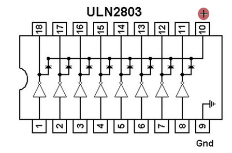
In the segment lines we need some way to reduce the current for the leds in out display and 470 Ohm is a very common value. You can lower or raise this value a little to make the displays light up brighter as you like. The ULN2803 is also very easy to wire on a breadboard, all the inputs are on one side and all the outputs on the other side, and compared to 8 transistors with a base resistor this chip takes up very little space.
Have fun, regards, Hein Pragt.
TTL IC Overview

This is a table with an overview of all TTL IC typenumbers and a short description of the chip. The chips are available in many variants such as LS and HC types, the operation is the same, but the electrical specifications are different. You cannot simply replace an LS with an HC type without being sure that the fan-in and fan-out and the threshold values have no effect.
List of TTL IC’s
| Part number | Description |
|---|---|
| 7400 | quad 2-input NAND gate |
| 7401 | quad 2-input NAND gate with open collector outputs |
| 7402 | quad 2-input NOR gate |
| 7403 | quad 2-input NAND gate with open collector outputs |
| 7404 | hex inverter |
| 7405 | hex inverter with open collector outputs |
| 7406 | hex inverter buffer/driver with 30 V open collector outputs |
| 7407 | hex buffer/driver with 30 V open collector outputs |
| 7408 | quad 2-input AND gate |
| 7409 | quad 2-input AND gate with open collector outputs |
| 7410 | triple 3-input NAND gate |
| 7411 | triple 3-input AND gate |
| 7412 | triple 3-input NAND gate with open collector outputs |
| 7413 | dual Schmitt trigger 4-input NAND gate |
| 7414 | hex Schmitt trigger inverter |
| 7415 | triple 3-input AND gate with open collector outputs |
| 7416 | hex inverter buffer/driver with 15 V open collector outputs |
| 7417 | hex buffer/driver with 15 V open collector outputs |
| 7418 | dual 4-input NAND gate with Schmitt trigger inputs |
| 7419 | hex Schmitt trigger inverter |
| 7420 | dual 4-input NAND gate |
| 7421 | dual 4-input AND gate |
| 7422 | dual 4-input NAND gate with open collector outputs |
| 7423 | expandable dual 4-input NOR gate with strobe |
| 7424 | quad 2-input NAND gate gates with schmitt-trigger line-receiver inputs. |
| 7425 | dual 4-input NOR gate with strobe |
| 7426 | quad 2-input NAND gate with 15 V open collector outputs |
| 7427 | triple 3-input NOR gate |
| 7428 | quad 2-input NOR buffer |
| 7430 | 8-input NAND gate |
| 7431 | hex delay elements |
| 7432 | quad 2-input OR gate |
| 7433 | quad 2-input NOR buffer with open collector outputs |
| 7434 | hex noninverters |
| 7435 | hex noninverters with open-collector outputs |
| 7436 | quad 2-input NOR gate (different pinout than 7402) |
| 7437 | quad 2-input NAND buffer |
| 7438 | quad 2-input NAND buffer with open collector outputs |
| 7439 | quad 2-input NAND buffer with open collector outputs, input and output terminals flipped, otherwise functionally identical to 7438 |
| 7440 | dual 4-input NAND buffer |
| 7441 | BCD to decimal decoder/Nixie tube driver |
| 7442 | BCD to decimal decoder |
| 7443 | excess-3 to decimal decoder |
| 7444 | excess-3-Gray code to decimal decoder |
| 7445 | BCD to decimal decoder/driver |
| 7446 | BCD to seven-segment display decoder/driver with 30 V open collector outputs |
| 7447 | BCD to 7-segment decoder/driver with 15 V open collector outputs |
| 7448 | BCD to 7-segment decoder/driver with Internal Pullups |
| 7449 | BCD to 7-segment decoder/driver with open collector outputs |
| 7450 | dual 2-wide 2-input AND-OR-invert gate (one gate expandable) |
| 7451 | dual 2-wide 2-input AND-OR-invert gate |
| 7452 | expandable 4-wide 2-input AND-OR gate |
| 7453 | expandable 4-wide 2-input AND-OR-invert gate |
| 7454 | 3-2-2-3-input AND-OR-invert gate |
| 7455 | 2-wide 4-input AND-OR-invert Gate (74H version is expandable) |
| 7456 | 50:1 frequency divider |
| 7457 | 60:1 frequency divider |
| 7458 | 2-input & 3-input AND-OR Gate |
| 7459 | 2-input & 3-input AND-OR-invert Gate |
| 7460 | dual 4-input expander |
| 7461 | triple 3-input expander |
| 7462 | 3-2-2-3-input AND-OR expander |
| 7463 | hex current sensing interface gates |
| 7464 | 4-2-3-2-input AND-OR-invert gate |
| 7465 | 4-2-3-2 input AND-OR-invert gate with open collector output |
| 7468 | dual 4 bit decade counters |
| 7469 | dual 4 bit binary counters |
| 7470 | AND-gated positive edge triggered J-K flip-flop with preset and clear |
| 7471 | AND-or-gated J-K master-slave flip-flop with preset |
| 7472 | AND gated J-K master-slave flip-flop with preset and clear |
| 7473 | dual J-K flip-flop with clear |
| 7474 | dual D positive edge triggered flip-flop with preset and clear |
| 7475 | 4-bit bistable latch |
| 7476 | dual J-K flip-flop with preset and clear |
| 7477 | 4-bit bistable latch |
| 7478 | dual positive pulse triggered J-K flip-flop with preset, common clock, and common clear |
| 7479 | dual D flip-flop |
| 7480 | gated full adder |
| 7481 | 16-bit random access memory |
| 7482 | 2-bit binary full adder |
| 7483 | 4-bit binary full adder |
| 7484 | 16-bit random access memory |
| 7485 | 4-bit magnitude comparator |
| 7486 | quad 2-input XOR gate |
| 7487 | 4-bit true/complement/zero/one element |
| 7488 | 256-bit read-only memory |
| 7489 | 64-bit random access memory |
| 7490 | decade counter (separate divide-by-2 and divide-by-5 sections) |
| 7491 | 8-bit shift register, serial In, serial out, gated input |
| 7492 | divide-by-12 counter (separate divide-by-2 and divide-by-6 sections) |
| 7493 | 4-bit binary counter (separate divide-by-2 and divide-by-8 sections) |
| 7494 | 4-bit shift register, dual asynchronous presets |
| 7495 | 4-bit shift register, parallel In, parallel out, serial input |
| 7496 | 5-bit parallel-In/parallel-out shift register, asynchronous preset |
| 7497 | synchronous 6-bit binary rate multiplier |
| 7498 | 4-bit data selector/storage register |
| 7499 | 4-bit bidirectional universal shift register |
| 74100 | dual 4-bit bistable latch |
| 74101 | AND-OR-gated J-K negative-edge-triggered flip-flop with preset |
| 74102 | AND-gated J-K negative-edge-triggered flip-flop with preset and clear |
| 74103 | dual J-K negative-edge-triggered flip-flop with clear |
| 74104 | J-K master-slave flip-flop |
| 74105 | J-K master-slave flip-flop |
| 74106 | dual J-K negative-edge-triggered flip-flop with preset and clear |
| 74107 | dual J-K flip-flop with clear |
| 74108 | dual J-K negative-edge-triggered flip-flop with preset, common clear, and common clock |
| 74109 | dual J-Not-K positive-edge-triggered flip-flop with clear and preset |
| 74110 | AND-gated J-K master-slave flip-flop with data lockout |
| 74111 | dual J-K master-slave flip-flop with data lockout |
| 74112 | dual J-K negative-edge-triggered flip-flop with clear and preset |
| 74113 | dual J-K negative-edge-triggered flip-flop with preset |
| 74114 | dual J-K negative-edge-triggered flip-flop with preset, common clock and clear |
| 74116 | dual 4-bit latch with clear |
| 74118 | hex set/reset latch |
| 74119 | hex set/reset latch |
| 74120 | dual pulse synchronizer/drivers |
| 74121 | monostable multivibrator |
| 74122 | retriggerable monostable multivibrator with clear |
| 74123 | dual retriggerable monostable multivibrator with clear |
| 74124 | dual voltage-controlled oscillator |
| 74125 | quad bus buffer with three-state outputs, negative enable |
| 74126 | quad bus buffer with three-state outputs, positive enable |
| 74128 | quad 2-input NOR Line driver |
| 74130 | quad 2-input AND gate buffer with 30 V open collector outputs |
| 74131 | quad 2-input AND gate buffer with 15 V open collector outputs |
| 74132 | quad 2-input NAND schmitt trigger |
| 74133 | 13-input NAND gate |
| 74134 | 12-input NAND gate with three-state output |
| 74135 | quad exclusive-or/NOR gate |
| 74136 | quad 2-input XOR gate with open collector outputs |
| 74137 | 3 to 8-line decoder/demultiplexer with address latch |
| 74138 | 3 to 8-line decoder/demultiplexer |
| 74139 | dual 2 to 4-line decoder/demultiplexer |
| 74140 | dual 4-input NAND line driver |
| 74141 | BCD to decimal decoder/driver for cold-cathode indicator/Nixie tube |
| 74142 | decade counter/latch/decoder/driver for Nixie tubes |
| 74143 | decade counter/latch/decoder/7-segment driver, 15 ma constant current |
| 74144 | decade counter/latch/decoder/7-segment driver, 15 V open collector outputs |
| 74145 | BCD to decimal decoder/driver |
| 74147 | 10-line to 4-line priority encoder |
| 74148 | 8-line to 3-line priority encoder |
| 74150 | 16-line to 1-line data selector/multiplexer |
| 74151 | 8-line to 1-line data selector/multiplexer |
| 74152 | 8-line to 1-line data selector/multiplexer |
| 74153 | dual 4-line to 1-line data selector/multiplexer |
| 74154 | 4-line to 16-line decoder/demultiplexer |
| 74155 | dual 2-line to 4-line decoder/demultiplexer |
| 74156 | dual 2-line to 4-line decoder/demultiplexer with open collector outputs |
| 74157 | quad 2-line to 1-line data selector/multiplexer, noninverting |
| 74158 | quad 2-line to 1-line data selector/multiplexer, inverting |
| 74159 | 4-line to 16-line decoder/demultiplexer with open collector outputs |
| 74160 | synchronous 4-bit decade counter with asynchronous clear |
| 74161 | synchronous 4-bit binary counter with asynchronous clear |
| 74162 | synchronous 4-bit decade counter with synchronous clear |
| 74163 | synchronous 4-bit binary counter with synchronous clear |
| 74164 | 8-bit parallel-out serial shift register with asynchronous clear |
| 74165 | 8-bit serial shift register, parallel Load, complementary outputs |
| 74166 | parallel-Load 8-bit shift register |
| 74167 | synchronous decade rate multiplier |
| 74168 | synchronous 4-bit up/down decade counter |
| 74169 | synchronous 4-bit up/down binary counter |
| 74170 | 4 by 4 register file with open collector outputs |
| 74171 | quad D-type flip-flops with clear |
| 74172 | 16-bit multiple port register file with three-state outputs |
| 74173 | quad d flip-flop with three-state outputs |
| 74174 | hex d flip-flop with common clear |
| 74175 | quad d edge-triggered flip-flop with complementary outputs and asynchronous clear |
| 74176 | presettable decade (bi-quinary) counter/latch |
| 74177 | presettable binary counter/latch |
| 74178 | 4-bit parallel-access shift register |
| 74179 | 4-bit parallel-access shift register with asynchronous clear and complementary Qd outputs |
| 74180 | 9-bit odd/even parity bit generator and checker |
| 74181 | 4-bit arithmetic logic unit and function generator |
| 74182 | lookahead carry generator |
| 74183 | dual carry-save full adder |
| 74184 | BCD to binary converter |
| 74185 | 6-bit binary to BCD converter |
| 74186 | 512-bit (64×8) read-only memory with open collector outputs |
| 74187 | 1024-bit (256×4) read only memory with open collector outputs |
| 74188 | 256-bit (32×8) programmable read-only memory with open collector outputs |
| 74189 | 64-bit (16×4) RAM with inverting three-state outputs |
| 74190 | synchronous up/down decade counter |
| 74191 | synchronous up/down binary counter |
| 74192 | synchronous up/down decade counter with clear |
| 74193 | synchronous up/down 4-bit binary counter with clear |
| 74194 | 4-bit bidirectional universal shift register |
| 74195 | 4-bit parallel-access shift register |
| 74196 | presettable decade counter/latch |
| 74197 | presettable binary counter/latch |
| 74198 | 8-bit bidirectional universal shift register |
| 74199 | 8-bit bidirectional universal shift register with J-Not-K serial inputs |
| 74200 | 256-bit ram with three-state outputs |
| 74201 | 256-bit (256×1) ram with three-state outputs |
| 74206 | 256-bit ram with open collector outputs |
| 74209 | 1024-bit (1024×1) ram with three-state output |
| 74210 | octal buffer |
| 74219 | 64-bit (16×4) RAM with noninverting three-state outputs |
| 74221 | dual monostable multivibrator with schmitt trigger input |
| 74222 | 16 by 4 synchronous FIFO memory with three-state outputs |
| 74224 | 16 by 4 synchronous FIFO memory with three-state outputs |
| 74225 | asynchronous 16×5 FIFO memory |
| 74226 | 4-bit parallel latched bus transceiver with three-state outputs |
| 74227 | 64-bit fifo memories 16×4 |
| 74228 | 64-bit fifo memories 16×4 open-collector outputs |
| 74230 | octal buffer/driver with three-state outputs, true and complementary inputs |
| 74231 | octal buffer and line driver with three-state outputs, G and /G complementary inputs |
| 74232 | quad NOR Schmitt trigger |
| 74237 | 3-of-8 decoder/demultiplexer with address latch, active high outputs |
| 74238 | 3-of-8 decoder/demultiplexer, active high outputs |
| 74239 | dual 2-of-4 decoder/demultiplexer, active high outputs |
| 74240 | octal buffer with Inverted three-state outputs |
| 74241 | octal buffer with noninverted three-state outputs |
| 74242 | quad bus transceiver with Inverted three-state outputs |
| 74243 | quad bus transceiver with noninverted three-state outputs |
| 74244 | octal buffer with noninverted three-state outputs |
| 74245 | octal bus transceiver with noninverted three-state outputs |
| 74246 | BCD to 7-segment decoder/driver with 30 V open collector outputs |
| 74247 | BCD to 7-segment decoder/driver with 15 V open collector outputs |
| 74248 | BCD to 7-segment decoder/driver with Internal Pull-up outputs |
| 74249 | BCD to 7-segment decoder/driver with open collector outputs |
| 74250 | 1 of 16 data selectors/multiplexers |
| 74251 | 8-line to 1-line data selector/multiplexer with complementary three-state outputs |
| 74253 | dual 4-line to 1-line data selector/multiplexer with three-state outputs |
| 74255 | dual 4-bit addressable latch |
| 74256 | dual 4-bit addressable latch |
| 74257 | quad 2-line to 1-line data selector/multiplexer with noninverted three-state outputs |
| 74258 | quad 2-line to 1-line data selector/multiplexer with Inverted three-state outputs |
| 74259 | 8-bit addressable latch |
| 74260 | dual 5-input NOR gate |
| 74261 | 2-bit by 4-bit parallel binary multiplier |
| 74264 | look ahead carry generator |
| 74265 | quad complementary output elements |
| 74266 | quad 2-input XNOR gate with open collector outputs |
| 74268 | hex d-type latches three-state outputs, common output control, common enable |
| 74270 | 2048-bit (512×4) read only memory with open collector outputs |
| 74271 | 2048-bit (256×8) read only memory with open collector outputs |
| 74273 | 8-bit register with reset |
| 74274 | 4-bit by 4-bit binary multiplier |
| 74275 | 7-bit slice Wallace tree |
| 74276 | quad J-Not-K edge-triggered Flip-Flops with separate clocks, common preset and clear |
| 74278 | 4-bit cascadeable priority registers with latched data inputs |
| 74279 | quad set-reset latch |
| 74280 | 9-bit odd/even Parity bit Generator/checker |
| 74281 | 4-bit parallel binary accumulator |
| 74282 | look-ahead carry generator with selectable carry inputs |
| 74283 | 4-bit binary Full adder |
| 74284 | 4-bit by 4-bit parallel binary multiplier (low order 4 bits of product) |
| 74285 | 4-bit by 4-bit parallel binary multiplier (high order 4 bits of product) |
| 74286 | 9-bit parity generator/checker with bus driver parity I/O port |
| 74287 | 1024-bit (256×4) programmable read-only memory with three-state outputs |
| 74288 | 256-bit (32×8) programmable read-only memory with three-state outputs |
| 74289 | 64-bit (16×4) RAM with open collector outputs |
| 74290 | decade counter (separate divide-by-2 and divide-by-5 sections) |
| 74291 | 4-bit universal shift register, binary up/down counter, synchronous |
| 74292 | programmable frequency divider/digital timer |
| 74293 | 4-bit binary counter (separate divide-by-2 and divide-by-8 sections) |
| 74294 | programmable frequency divider/digital timer |
| 74295 | 4-bit bidirectional register with three-state outputs |
| 74297 | digital phase-locked-loop filter |
| 74298 | quad 2-input multiplexer with storage |
| 74299 | 8-bit bidirectional universal shift/storage register with three-state outputs |
| 74301 | 256-bit (256×1) random access memory with open collector output |
| 74309 | 1024-bit (1024×1) random access memory with open collector output |
| 74310 | octal buffer with Schmitt trigger inputs |
| 74314 | 1024-bit random access memory |
| 74319 | 64-bit random access memories 16×4 open collector outputs |
| 74320 | crystal controlled oscillator |
| 74321 | crystal-controlled oscillators with F/2 and F/4 count-down outputs |
| 74322 | 8-bit shift register with sign extend, three-state outputs |
| 74323 | 8-bit bidirectional universal shift/storage register with three-state outputs |
| 74324 | voltage controlled oscillator (or crystal controlled) |
| 74340 | octal buffer with Schmitt trigger inputs and three-state inverted outputs |
| 74341 | octal buffer with Schmitt trigger inputs and three-state noninverted outputs |
| 74344 | octal buffer with Schmitt trigger inputs and three-state noninverted outputs |
| 74347 | bcd to seven segment decoders/drivers open collector outputs, low voltage version of 7447 |
| 74348 | 8 to 3-line priority encoder with three-state outputs |
| 74350 | 4-bit shifter with three-state outputs |
| 74351 | dual 8-line to 1-line data selectors/multiplexers with three-state outputs and 4 common data inputs |
| 74352 | dual 4-line to 1-line data selectors/multiplexers with inverting outputs |
| 74353 | dual 4-line to 1-line data selectors/multiplexers with inverting three-state outputs |
| 74354 | 8 to 1-line data selector/multiplexer with transparent latch, three-state outputs |
| 74355 | 8-line to 1-line data selector/multiplexer with transparent registers, open-collector outputs |
| 74356 | 8 to 1-line data selector/multiplexer with edge-triggered register, three-state outputs |
| 74357 | 8-line to 1-line data selectors/multiplexers/edge-triggered registers, open-collector outputs |
| 74361 | bubble memory function timing generator |
| 74362 | four-phase clock generator/driver |
| 74363 | octal three-state D-latches |
| 74365 | hex buffer with noninverted three-state outputs |
| 74366 | hex buffer with Inverted three-state outputs |
| 74367 | hex buffer with noninverted three-state outputs |
| 74368 | hex buffer with Inverted three-state outputs |
| 74370 | 2048-bit (512×4) read-only memory with three-state outputs |
| 74371 | 2048-bit (256×8) read-only memory with three-state outputs |
| 74373 | octal transparent latch with three-state outputs |
| 74374 | octal register with three-state outputs |
| 74375 | quad bistable latch |
| 74376 | quad J-Not-K flip-flop with common clock and common clear |
| 74377 | 8-bit register with clock enable |
| 74378 | 6-bit register with clock enable |
| 74379 | 4-bit register with clock enable and complementary outputs |
| 74380 | 8-bit multifunction register |
| 74381 | 4-bit arithmetic logic unit/function generator with generate and propagate outputs |
| 74382 | 4-bit arithmetic logic unit/function generator with ripple carry and overflow outputs |
| 74384 | 8-bit by 1-bit two’s complement multipliers |
| 74385 | quad 4-bit adder/subtractor |
| 74386 | quad 2-input XOR gate |
| 74387 | 1024-bit (256×4) programmable read-only memory with open collector outputs |
| 74388 | 4-bit register with standard and three-state outputs |
| 74390 | dual 4-bit decade counter |
| 74393 | dual 4-bit binary counter |
| 74395 | 4-bit universal shift register with three-state outputs |
| 74396 | octal storage registers, parallel access |
| 74398 | quad 2-input multiplexers with storage and complementary outputs |
| 74399 | quad 2-input multiplexer with storage |
| 74405 | 1 to 8 decoder, equivalent to Intel 8205, only found as UCY74S405 so might be non-TI number |
| 74408 | 8-bit parity tree |
| 74412 | multi-mode buffered 8-bit latches with three-state outputs and clear |
| 74422 | re-triggerable mono-stable multivibrators, two inputs |
| 74423 | dual retriggerable monostable multivibrator |
| 74424 | two-phase clock generator/driver |
| 74425 | quad gates with three-state outputs and active low enables |
| 74426 | quad gates with three-state outputs and active high enables |
| 74428 | system controller for 8080a |
| 74436 | line driver/memory driver circuits – mos memory interface, damping output resistor |
| 74437 | line driver/memory driver circuits – mos memory interface |
| 74438 | system controller for 8080a |
| 74440 | quad tridirectional bus transceiver with noninverted open collector outputs |
| 74441 | quad tridirectional bus transceiver with Inverted open collector outputs |
| 74442 | quad tridirectional bus transceiver with noninverted three-state outputs |
| 74443 | quad tridirectional bus transceiver with Inverted three-state outputs |
| 74444 | quad tridirectional bus transceiver with Inverted and noninverted three-state outputs |
| 74445 | bcd-to-decimal decoders/drivers |
| 74446 | quad bus transceivers with direction controls |
| 74447 | bcd-to-seven-segment decoders/drivers, low voltage version of 74247 |
| 74448 | quad tridirectional bus transceiver with Inverted and noninverted open collector outputs |
| 74449 | quad bus transceivers with direction controls, true outputs |
| 74450 | 16-to-1 multiplexer with complementary outputs |
| 74451 | dual 8-to-1 multiplexer |
| 74452 | dual decade counter, synchronous |
| 74453 | dual binary counter, synchronous |
| 74453 | quad 4-to-1 multiplexer |
| 74454 | dual decade up/down counter, synchronous, preset input |
| 74455 | dual binary up/down counter, synchronous, preset input |
| 74456 | NBCD (Natural binary coded decimal) adder |
| 74460 | bus transfer switch |
| 74461 | 8-bit presettable binary counter with three-state outputs |
| 74462 | fiber-optic link transmitter |
| 74463 | fiber-optic link receiver |
| 74465 | octal buffer with three-state true outputs |
| 74466 | octal buffers with three-state inverted outputs |
| 74467 | octal buffers with three-state true outputs |
| 74468 | octal buffers with three-state inverted outputs |
| 74470 | 2048-bit (256×8) programmable read-only memory with open collector outputs |
| 74471 | 2048-bit (256×8) programmable read-only memory with three-state outputs |
| 74472 | programmable read-only memory with open collector outputs |
| 74473 | programmable read-only memory with three-state outputs |
| 74474 | programmable read-only memory with open collector outputs |
| 74475 | programmable read-only memory with three-state outputs |
| 74481 | 4-bit slice cascadable processor elements |
| 74482 | 4-bit slice expandable control elements |
| 74484 | BCD-to-binary converter |
| 74485 | binary-to-BCD converter |
| 74490 | dual decade counter |
| 74491 | 10-bit binary up/down counter with limited preset and three-state outputs |
| 74498 | 8-bit bidirectional shift register with parallel inputs and three-state outputs |
| 74508 | 8-bit multiplier/divider |
| 74518 | 8-bit comparator with open collector output, input pull-up resistor |
| 74519 | 8-bit comparator with open collector output |
| 74520 | 8-bit comparator with inverted totem-pole output, input pull-up resistor |
| 74521 | 8-bit comparator with inverted totem-pole output |
| 74522 | 8-bit comparator with inverted open-collector output, input pull-up resistor |
| 74526 | fuse programmable identity comparator, 16 bit |
| 74527 | fuse programmable identity comparator, 8 bit + 4 bit conventional Identity comparator |
| 74528 | fuse programmable Identity comparator, 12 bit |
| 74531 | octal transparent latch with 32 ma three-state outputs |
| 74532 | octal register with 32 ma three-state outputs |
| 74533 | octal transparent latch with inverting three-state outputs |
| 74534 | octal register with inverting three-state outputs |
| 74535 | octal transparent latch with inverting three-state outputs |
| 74536 | octal register with inverting 32 ma three-state outputs |
| 74537 | BCD to decimal decoder with three-state outputs |
| 74538 | 1 of 8 decoder with three-state outputs |
| 74539 | dual 1 of 4 decoder with three-state outputs |
| 74540 | inverting octal buffer with three-state outputs |
| 74541 | non-inverting octal buffer with three-state outputs |
| 74544 | non-inverting octal registered transceiver with three-state outputs |
| 74558 | 8-bit by 8-bit multiplier with three-state outputs |
| 74560 | 4-bit decade counter with three-state outputs |
| 74561 | 4-bit binary counter with three-state outputs |
| 74563 | 8-bit d-type transparent latch with inverting three-state outputs |
| 74564 | 8-bit d-type edge-triggered register with inverting three-state outputs |
| 74568 | decade up/down counter with three-state outputs |
| 74569 | binary up/down counter with three-state outputs |
| 74573 | octal D-type transparent latch with three-state outputs |
| 74574 | octal D-type edge-triggered flip-flop with three-state outputs |
| 74575 | octal D-type flip-flop with synchronous clear, three-state outputs |
| 74576 | octal D-type flip-flop with inverting three-state outputs |
| 74577 | octal D-type flip-flop with synchronous clear, inverting three-state outputs |
| 74580 | octal transceiver/latch with inverting three-state outputs |
| 74589 | 8-bit shift register with input latch, three-state outputs |
| 74590 | 8-bit binary counter with output registers and three-state outputs |
| 74591 | 8-bit binary counters with output registers, open-collector outputs |
| 74592 | 8-bit binary counter with input registers |
| 74593 | 8-bit binary counter with input registers and three-state outputs |
| 74594 | 8-bit shift registers with output latches |
| 74595 | 8-bit shift registers with output latches, three-state parallel outputs |
| 74596 | 8-bit shift registers with output latches, open-collector parallel outputs |
| 74597 | 8-bit shift registers with input latches |
| 74598 | 8-bit shift register with input latches |
| 74599 | 8-bit shift registers with output latches, open-collector outputs |
| 74600 | dynamic memory refresh controller, transparent and burst modes, for 4K or 16K drams |
| 74601 | dynamic memory refresh controller, transparent and burst modes, for 64K drams |
| 74602 | dynamic memory refresh controller, cycle steal and burst modes, for 4K or 16K drams |
| 74603 | dynamic memory refresh controller, cycle steal and burst modes, for 64K drams |
| 74604 | octal 2-input multiplexer with latch, high-speed, with three-state outputs |
| 74605 | latch, high-speed, with open collector outputs |
| 74606 | octal 2-input multiplexer with latch, glitch-free, with three-state outputs |
| 74607 | octal 2-input multiplexer with latch, glitch-free, with open collector outputs |
| 74608 | memory cycle controller |
| 74610 | memory mapper, latched, three-state outputs |
| 74611 | memory mapper, latched, open collector outputs |
| 74612 | memory mapper, three-state outputs |
| 74613 | memory mapper, open collector outputs |
| 74618 | Schmitt-trigger positive-nand gates with totem-pole outputs |
| 74619 | Schmitt-trigger inverters with totem-pole outputs |
| 74620 | octal bus transceiver, inverting, three-state outputs |
| 74621 | octal bus transceiver, noninverting, open collector outputs |
| 74622 | octal bus transceiver, inverting, open collector outputs |
| 74623 | octal bus transceiver, noninverting, three-state outputs |
| 74624 | voltage-controlled oscillator with enable control, range control, two-phase outputs |
| 74625 | dual voltage-controlled oscillator with two-phase outputs |
| 74626 | dual voltage-controlled oscillator with enable control, two-phase outputs |
| 74627 | dual voltage-controlled oscillator |
| 74628 | voltage-controlled oscillator with enable control, range control, external temperature compensation, and two-phase outputs |
| 74629 | dual voltage-controlled oscillator with enable control, range control |
| 74630 | 16-bit error detection and correction (EDAC) with three-state outputs |
| 74631 | 16-bit error detection and correction with open collector outputs |
| 74632 | 32-bit parallel error detection and correction, three-state outputs, byte-write |
| 74633 | 32-bit parallel error detection and correction, open-collector outputs, byte-write |
| 74634 | 32-bit parallel error detection and correction, three-state outputs |
| 74635 | 32-bit parallel error detection and correction, open-collector outputs |
| 74638 | octal bus transceiver with inverting three-state outputs |
| 74639 | octal bus transceiver with noninverting three-state outputs |
| 74640 | octal bus transceiver with inverting three-state outputs |
| 74641 | octal bus transceiver with noninverting open collector outputs |
| 74642 | octal bus transceiver with inverting open collector outputs |
| 74643 | octal bus transceiver with mix of inverting and noninverting three-state outputs |
| 74644 | octal bus transceiver with mix of inverting and noninverting open collector outputs |
| 74645 | octal bus transceiver |
| 74646 | octal bus transceiver/latch/multiplexer with noninverting three-state outputs |
| 74647 | octal bus transceiver/latch/multiplexer with noninverting open collector outputs |
| 74648 | octal bus transceiver/latch/multiplexer with inverting three-state outputs |
| 74649 | octal bus transceiver/latch/multiplexer with inverting open collector outputs |
| 74651 | octal bus transceiver/register with inverting three-state outputs |
| 74652 | octal bus transceiver/register with noninverting three-state outputs |
| 74653 | octal bus transceiver/register with inverting three-state and open collector outputs |
| 74654 | octal bus transceiver/register with noninverting three-state and open collector outputs |
| 74658 | octal bus transceiver with Parity, inverting |
| 74659 | octal bus transceiver with Parity, noninverting |
| 74664 | octal bus transceiver with Parity, inverting |
| 74665 | octal bus transceiver with Parity, noninverting |
| 74668 | synchronous 4-bit decade Up/down counter |
| 74669 | synchronous 4-bit binary Up/down counter |
| 74670 | 4 by 4 register File with three-state outputs |
| 74671 | 4-bit bidirectional shift register/latch /multiplexer with three-state outputs |
| 74672 | 4-bit bidirectional shift register/latch/multiplexer with three-state outputs |
| 74673 | 16-bit serial-in serial-out shift register with output storage registers, three-state outputs |
| 74674 | 16-bit parallel-in serial-out shift register with three-state outputs |
| 74677 | 16-bit address comparator with enable |
| 74678 | 16-bit address comparator with latch |
| 74679 | 12-bit address comparator with latch |
| 74680 | 12-bit address comparator with enable |
| 74681 | 4-bit parallel binary accumulator |
| 74682 | 8-bit magnitude comparator |
| 74683 | 8-bit magnitude comparator with open collector outputs |
| 74684 | 8-bit magnitude comparator |
| 74685 | 8-bit magnitude comparator with open collector outputs |
| 74686 | 8-bit magnitude comparator with enable |
| 74687 | 8-bit magnitude comparator with enable |
| 74688 | 8-bit equality comparator |
| 74689 | 8-bit magnitude comparator with open collector outputs |
| 74690 | three-state outputs |
| 74691 | 4-bit binary counter/latch/multiplexer with asynchronous reset, three-state outputs |
| 74692 | 4-bit decimal counter/latch/multiplexer with synchronous reset, three-state outputs |
| 74693 | 4-bit binary counter/latch/multiplexer with synchronous reset, three-state outputs |
| 74694 | 4-bit decimal counter/latch/multiplexer with synchronous and asynchronous resets, three-state outputs |
| 74695 | 4-bit binary counter/latch/multiplexer with synchronous and asynchronous resets, three-state outputs |
| 74696 | 4-bit decimal counter/register/multiplexer with asynchronous reset, three-state outputs |
| 74697 | 4-bit binary counter/register/multiplexer with asynchronous reset, three-state outputs |
| 74698 | 4-bit decimal counter/register/multiplexer with synchronous reset, three-state outputs |
| 74699 | 4-bit binary counter/register/multiplexer with synchronous reset, three-state outputs |
| 74716 | programmable decade counter |
| 74718 | programmable binary counter |
| 74724 | voltage controlled multivibrator |
| 74740 | octal buffer/Line driver, inverting, three-state outputs |
| 74741 | octal buffer/Line driver, noninverting, three-state outputs, mixed enable polarity |
| 74744 | octal buffer/Line driver, noninverting, three-state outputs |
| 74748 | 8 to 3-line priority encoder |
| 74779 | 8-bit bidirectional binary counter (three-state) |
| 74783 | synchronous address multiplexer |
| 74790 | error detection and correction (EDAC) |
| 74794 | 8-bit register with readback |
| 74795 | octal buffer with three-state outputs |
| 74796 | octal buffer with three-state outputs |
| 74797 | octal buffer with three-state outputs |
| 74798 | octal buffer with three-state outputs |
| 74804 | hex 2-input NAND drivers |
| 74805 | hex 2-input NOR drivers |
| 74808 | hex 2-input AND drivers |
| 74822 | 10-bit bus interface flipflop with three-state outputs |
| 74832 | hex 2-input OR drivers |
| 74848 | 8 to 3-line priority encoder with three-state outputs |
| 74873 | octal transparent latch |
| 74874 | octal d-type flip-flop |
| 74876 | octal d-type flip-flop with inverting outputs |
| 74878 | dual 4-bit d-type flip-flop with synchronous clear, noninverting three-state outputs |
| 74879 | dual 4-bit d-type flip-flop with synchronous clear, inverting three-state outputs |
| 74880 | octal transparent latchwith inverting outputs |
| 74881 | arithmetic logic unit |
| 74882 | 32-bit lookahead carry generator |
| 74888 | 8-bit slice processor |
| 74901 | hex inverting TTL buffer |
| 74902 | hex non-inverting TTL buffer |
| 74903 | hex inverting CMOS buffer |
| 74904 | hex non-inverting CMOS buffer |
| 74905 | 12-Bit successive approximation register |
| 74906 | hex open drain n-channel buffers |
| 74907 | hex open drain p-channel buffers |
| 74908 | dual CMOS 30 V relay driver |
| 74909 | quad voltage comparator |
| 74910 | 256×1 CMOS static RAM |
| 74911 | 4 digit expandable display controller |
| 74912 | 6 digit BCD display controller and driver |
| 74914 | hex schmitt trigger with extended input voltage |
| 74915 | seven segment to BCD decoder |
| 74917 | 6 digit Hex display controller and driver |
| 74918 | dual CMOS 30 V relay driver |
| 74920 | 256×4 CMOS static RAM |
| 74921 | 256×4 CMOS static RAM |
| 74922 | 16-key encoder |
| 74923 | 20-key encoder |
| 74925 | 4-digit counter/display driver |
| 74926 | 4-digit counter/display driver |
| 74927 | 4-digit counter/display driver |
| 74928 | 4-digit counter/display driver |
| 74929 | 1024×1 CMOS static RAM |
| 74930 | 1024×1 CMOS static RAM |
| 74932 | phase comparator |
| 74933 | address bus comparator |
| 74934 | =ADC0829 ADC, see corresponding NSC datasheet |
| 74935 | 3.5-digit digital voltmeter (DVM) support chip for multiplexed 7-segment displays |
| 74936 | 3.75-digit digital voltmeter (DVM) support chip for multiplexed 7-segment displays |
| 74937 | =ADC3511 ADC, see corresponding NSC datasheet |
| 74938 | =ADC3711 ADC, see corresponding NSC datasheet |
| 74941 | octal bus/line drivers/line receivers |
| 74945 | 4 digit up/down counter with decoder and driver |
| 74947 | 4 digit up/down counter with decoder and driver |
| 74948 | =ADC0816 ADC, see corresponding NSC datasheet |
| 74949 | =ADC0808 ADC, see corresponding NSC datasheet |
| 741005 | hex inverting buffer with open-collector output |
| 741035 | hex noninverting buffers with open-collector outputs |
| 742960 | error detection and correction (EDAC) |
| 742961 | edac bus buffer, inverting |
| 742962 | edac bus buffer, noninverting |
| 742968 | dynamic memory controller |
| 742969 | memory timing controller for use with EDAC |
| 742970 | memory timing controller for use without EDAC |
| 744002 | dual 4-input NOR gate |
| 744015 | dual 4-bit shift registers |
| 744016 | quad bilateral switch |
| 744017 | 5-stage ÷10 Johnson counter |
| 744020 | 14-stage binary counter |
| 744024 | 7 stage ripple carry binary counter |
| 744028 | BCD to decimal decoder |
| 744040 | 12-stage binary ripple counter |
| 744046 | phase-locked loop and voltage-controlled oscillator |
| 744049 | hex inverting buffer |
| 744050 | hex buffer/converter (non-inverting) |
| 744051 | high-speed CMOS 8-channel analog multiplexer/demultiplexer |
| 744052 | dual 4-channel analog multiplexer/demultiplexers |
| 744053 | triple 2-channel analog multiplexer/demultiplexers |
| 744059 | programmable divide-by-N counter |
| 744060 | 14-stage binary ripple counter with oscillator |
| 744066 | quad bilateral switches |
| 744067 | 16-channel analog multiplexer/demultiplexer |
| 744075 | triple 3-input OR gate |
| 744078 | 8-input OR/NOR gate |
| 744094 | 8-bit three-state shift register/latch |
| 744316 | quad analog switch |
| 744351 | 8-channel analog multiplexer/demultiplexer with latch |
| 744353 | Triple 2-channel analog multiplexer/demultiplexer with latch |
| 744511 | BCD to 7-segment decoder |
| 744514 | 4-to-16 line decoder/demultiplexer with input latches |
| 744520 | dual 4-bit synchronous binary counter |
| 744538 | dual retriggerable precision monostable multivibrator |
| 747007 | hex buffer |
| 747266 | quad 2-input XNOR gate |
| 7429841 | 10-bit bus-interface D-type latch with three-state outputs |
| 7440103 | presettable 8-bit synchronous down counter |
| 7440105 | 4-bit by 16-word FIFO register |
Programming the ATTiny85

In this post I will explain how to program am ATTiny25/45/85 MCU. I really like the AVR chips, they are powerful, have enough flash and sram memory and have a lot of build in I/O devices. And the chips come in many sizes that all have the same MCU kernel, but a different number of I/O pins and different Flash/Sram sizes. The ATTiny85 is what I use the most, it has the most flash af the 25/45/85 series and it is rather cheap. The chip has 6 programmeble I/O pins and that is enough for a lot of things. It does not have a serial Uart but if you really need this you can use the software Uart. To program this chip you will need a programming environment, I use Visuals Studio PlatformIO and the old but decent Arduino IDE. Fot beginners I would recommend the Arduino IDE as it is foolproof and easier. With PlatformIO you can control much more (like all the fuse settings in binary format) but if you do something wrong you can get totally unusable bricked MCU chips. On this page I describe an Arduino Uno as ISP programmer.
Arduino Uno as ISP
I have bought a lot of Arduino programmers when I first started and I had a lot of problems with them especially the Chinese clones. Then I discovered the Arduino Uno as ISP and build several shields for 8, 14 , 20 and 28 pins AVR chips. Because all the different sizes of chips have their programming pins on different pins and need the power pins also connected, I build several shields. But they are cheap to make. Hier is the schematic of the shield I use for the ATTiny25/45/85 processor.
I use a standard prototype shield and a ZIF header for this (8 pins zif are hard to get so I use a bigger one and put tape on the unused pins), then first upload the Arduino as ISP scketch to the Arduino Uno. Select the AruidnoISP sketch from the examples and select Arduino Uno as board.


Connect the Arduino Uno using the USB cable and select the correct port in the Tools settings. Then use the Upload button to upload the ArduinoISP sketch to the Arduino Uno and your ISP programmer is ready.

I hope this was clear, if you got anything to add to this post then let me know, regards, Hein Pragt.
Programming the ATTiny2313

In this post I will explain how to program am ATTiny2313 / AT90S2313 MCU. I really like the AVR chips, they are powerful, have enough flash and sram memory and have a lot of build in I/O devices. And the chips come in many sizes that all have the same MCU kernel, but a different number of I/O pins and different Flash/Sram sizes. The ATTiny2313 (or the even cheaper AT90S2313) is just in the middle and I like to use this chip and it is not that expensive. To program this chip you will need a programming environment, I use Visuals Studio PlatformIO and the old but decent Arduino IDE. Fot beginners I would recommend the Arduino IDE as it is foolproof and easier. With PlatformIO you can control much more (like all the fuse settings in binary format) but if you do something wrong you can get totally unusable bricked MCU chips. On this page I describe an Arduino Uno as ISP programmer.
Arduino Uno as ISP
I have bought a lot of Arduino programmers when I first started and I had a lot of problems with them especially the Chinese clones. Then I discovered the Arduino Uno as ISP and build several shields for 8, 14 , 20 and 28 pins AVR chips. Because all the different sizes of chips have their programming pins on different pins and need the power pins also connected, I build several shields. But they are cheap to make. Hier is the schematic of the shield I use for the ATTiny2313 / AT90S2313 processor.

I use a standard prototype shield and a ZIF header for this, then first upload the Arduino as ISP scketch to the Arduino Uno. Select the AruidnoISP sketch from the examples and select Arduino Uno as board.
Connect the Arduino Uno using the USB cable and select the correct port in the Tools settings. Then use the Upload button to upload the ArduinoISP sketch to the Arduino Uno and your ISP programmer is ready.
I hope this was clear, if you got anything to add to this post then let me know, regards, Hein Pragt.
Programming the ATMega32A
In this post I will explain how to program am ATMega32A MCU. I really like the AVR chips, they are powerful, have enough flash and sram memory and have a lot of build in I/O devices. And the chips come in many sizes that all have the same MCU kernel, but a different number of I/O pins and different Flash/Sram sizes. If you really need a lot of I/O pins the ATMega32A is what you need, I like to use this chip and it is not that expensive. To program this chip you will need a programming environment, I use Visuals Studio PlatformIO and the old but decent Arduino IDE. Fot beginners I would recommend the Arduino IDE as it is foolproof and easier. With PlatformIO you can control much more (like all the fuse settings in binary format) but if you do something wrong you can get totally unusable bricked MCU chips. On this page I describe the Arduino IDE with an Arduino Uno as ISP programmer.
ARDUINO IDE

I really liked the Arduino IDE until the last versions. The (configuration / libraries) directories it uses are all over your disk and hard to find. That is why I recommend the portable arduino-1.8.19 version. This has all the files in a single directory. Install this version somewhere on your drive and it works out of the box. But out of the box it does not support the ATMega32 processors. There are several solutions that depend on your version of the Arduino IDE, find one that fits your IDE and install it. I have included this standard in my portable version of the Arduino IDE.
Arduino Uno as ISP
I have bought a lot of Arduino programmers when I first started and I had a lot of problems with them especially the Chinese clones. Then I discovered the Arduino Uno as ISP and build several shields for 8, 14 , 20 and 28 pins AVR chips. Because all the different sizes of chips have their programming pins on different pins and need the power pins also connected, I build several shields. But they are cheap to make. Hier is the schematic of the shield I use for the ATTin24 processor.

I use a standard prototype shield and a ZIF header for this, then first upload the Arduino as ISP scketch to the Arduino Uno. Select the AruidnoISP sketch from the examples and select Arduino Uno as board.
Connect the Arduino Uno using the USB cable and select the correct port in the Tools settings. Then use the Upload button to upload the ArduinoISP sketch to the Arduino Uno and your ISP programmer is ready.
Programming an ATMega32A
First we start by loading (or writing) the sourcecode file of the ATMega32 code in the programming language C in the Arduino IDE. Then go to the tools setting and select the correct device. Under tools select the configuration of the ATMega32A you will use, in my case an ATMega32 with external 16 Mhz clock.
// -----------------------------------------------
// Blink for ATMega32A
// H.M. Pragt 2022
// -----------------------------------------------

#ifndef F_CPU
#define F_CPU 16000000UL // 16 MHz clock speed
#endif

#include <avr/io.h>
#include <util/delay.h>

int main(void)
{
  DDRD = 0xFF; //Makes PORTD as Output
  while(1) //infinite loop
  {
    PORTD = 0xFF; //Turns ON All LEDs
    _delay_ms(2000); //1 second delay
    PORTD= 0x00; //Turns OFF All LEDs
    _delay_ms(2000); //1 second delay
  }
}
Now the last setting is selecting to use the ArduinoISP programmer:

Connect the Arduino Uno with the shield and the ATMega32A chip inserted to the computers and select upload button to program the code into the chip. As easy as that, happy programming.
I hope this was clear, if you got anything to add to this post then let me know, regards, Hein Pragt.
Programming the ATTiny24

In this post I will explain how to program am ATTiny24 (or 44,84) MCU. I really like the AVR chips, they are powerful, have enough flash and sram memory and have a lot of build in I/O devices. And the chips come in many sizes that all have the same MCU kernel, but a different number of I/O pins and different Flash/Sram sizes. I like to use the ATTiny85, it has 8 pins but of 6 I/O lines are enough this is a perfect MCU. The ATTiny2313 has 20 pins if you need more I/O lines, but the ATTiny24 has 14 pins and is cheap and has 12 programmable I/O lines. The small size with 12 I/O lines makes this one of my favorite AVR chips. To program this chip you will need a programming environment, I use Visuals Studio PlatformIO and the old but decent Arduino IDE. Fot beginners I would recommend the Arduino IDE as it is foolproof and easier. With PlatformIO you can control much more (like all the fuse settings in binary format) but if you do something wrong you can get totally unusable bricked MCU chips. On this page I describe the Arduino IDE with an Arduino Uno as ISP programmer.
ARDUINO IDE
I really liked the Arduino IDE until the last versions. The (configuration / libraries) directories it uses are all over your disk and hard to find. That is why I recommend the portable arduino-1.8.19 version. This has all the files in a single directory. Install this version somewhere on your drive and it works out of the box. But out of the box it does not support the ATTiny processors. Install a ATTiny core package like the https://github.com/damellis/attiny (I used this one). On this website is also an installation manual so I recommend you follow this. After this you will have a Arduino IDE that can program ATTiny24 / 44 / 84 chips. I have included this standard in my portable version of the Arduino IDE.
Arduino Uno as ISP
I have bought a lot of Arduino programmers when I first started and I had a lot of problems with them especially the Chinese clones. Then I discovered the Arduino Uno as ISP and build several shields for 8, 14 , 20 and 28 pins AVR chips. Because all the different sizes of chips have their programming pins on different pins and need the power pins also connected, I build several shields. But they are cheap to make. Hier is the schematic of the shield I use for the ATTin24 processor.

I use a standard prototype shield and a ZIF header for this, then first upload the Arduino as ISP scketch to the Arduino Uno. Select the AruidnoISP sketch from the examples and select Arduino Uno as board.
Connect the Arduino Uno using the USB cable and select the correct port in the Tools settings. Then use the Upload button to upload the ArduinoISP sketch to the Arduino Uno and your ISP programmer is ready.
Programming an ATTiny24
First we start by loading (or writing) the sourcecode file of the ATTinty code in the programming language C in the Arduino IDE. Then go to the tools setting and select the correct device.

Then select the internal or external clock and the frequency.

Now the last setting is selecting to use the ArduinoISP programmer:
Connect the Arduino Uno with the shield and the ATTiny24A chip inserted to the computers and select upload button to program the code into the chip. As easy as that, happy programming.
I hope this was clear, if you got anything to add to this post then let me know, regards, Hein Pragt.
Five way pushbutton latch

As a former hardware designer and embedded programmer I still like a little challenge. I design and build my own devices here are home but sometimes I get asked for a solution to a electronic design problem. When I was working as a designer there was always the challenge of my boss wanting to reduce the hardware, he said if you can fix it in software it will only cost me once, if you fix it in hardware it will cost me on every device. He could drive me crazy when he had been to the golf course and someone had convinced him to buy an even cheaper chip (that was not compatible most of the time) and I had to fix this in software. It created my way of thinking right now, be creative and use as less hardware resources as possible.
Someone asked me for a simple circuit that had five input pushbuttons and five output lines and when a button was pushed the corresponding output line had to go high. This is basically a latch function. There was one restriction, there may only be one output line active at the same time. You could create a circuit with traditional components but you would need a lot of resistors and diodes and transistors or a logical IC to do this. So a microcontroller option seemed the best solution. A PIC chip could do this, but I am not a big PIC fan, I like the AVR chips. My first idea was a ATTiny2313, as I had a few of them. This chip as an internal oscillator and internal pullups so a bare chip could do the job. I wrote some code using PlatformIO and downloaded that into a chip. It works as planned, the design and the code are below, there is also a zip file with the code of the PlatformIO project.

// -----------------------------------------------------
// Read 5 inputs and latch this input to the output
// Only one output can be active at the same time
// PA0 PA1  PD2 PD3 PD4 are inputs
// PB1 PB2 PB3 PB4 PB5  are outputs
// ------------------------------------------------------

#include <Arduino.h>

void setHigh(int prt);

// -----------------------------
// Init hardware
// -----------------------------

void setup()
{
    PORTA = _BV(PA0) | _BV(PA1);             // Set input + pullup
    PORTD = _BV(PD2) | _BV(PD3) | _BV(PD4);  // Set input + pullup
    DDRB = 0xff; // All pins of portB as output
    setHigh(1);
}


// -----------------------------------
// Main loop scan inputs
// -----------------------------------
void loop()
{
   while (-1) {
     if (~PINA & 0x02) {
        setHigh(1);
        continue;    // Prevent two keys at the same time
     }
     if (~PINA & 0x01) {
        setHigh(2);
        continue;
     }
     if (~PIND & 0x04) {
        setHigh(3);
        continue;
     }
     if (~PIND & 0x08) {
        setHigh(4);
        continue;
     }
     if (~PIND & 0x10) {
        setHigh(5);
        continue;
     }
   }
}

// ------------------------------------
// Set one ouput high 1..5
// ------------------------------------
void setHigh(int prt)
{
   PORTB = 0; // All off
   switch(prt) {
    case 1: PORTB |= 0x20;
            break;
    case 2: PORTB |= 0x10;
            break;
    case 3: PORTB |= 0x08;
            break;
    case 4: PORTB |= 0x04;
            break;
    case 5: PORTB |= 0x02;
            break;
   }
}Even smaller design
Then my old habit started to come up and I saw the unused pins and thought this is a shame, a ATTiny24A with only 14 pins could do the same. So I went back to the beginning and rewired the breadboard for a ATTiny24A. I created a new project in PlatformIO and reused the old code. This also works, so you can use whatever chip is cheaper, both do the same. This design and the code are also below, there is also a zip file with the code of the PlatformIO project. These designs and code are free to use, there is no copyright.

// -----------------------------------------------------
// Read 5 inputs and latch this input to the output
// Only one output can be active at the same time
// PB0 PB1 PB2 PA7 PA6 are inputs
// PA1 PA2 PA3 PA4 PA5  are outputs
// ------------------------------------------------------

#include <Arduino.h>

void setHigh(int prt);

// -----------------------------
// Init hardware
// -----------------------------

void setup()
{
    PORTB = _BV(PB0) | _BV(PB1) |_BV(PB2);  // Set input + pullup
    PORTA = _BV(PA7) | _BV(PA6);  // Set input + pullup
    DDRA = 0x3f; // All pins of portA as output exept 6 and 7
    setHigh(1);
}


// -----------------------------------
// Main loop scan inputs
// -----------------------------------
void loop()
{
   while (-1) {
     if (~PINB & 0x01) {
        setHigh(1);
        continue;    // Prevent two keys at the same time
     }
     if (~PINB & 0x02) {
        setHigh(2);
        continue;
     }
     if (~PINB & 0x04) {
        setHigh(3);
        continue;
     }
     if (~PINA & 0x80) {
        setHigh(4);
        continue;
     }
     if (~PINA & 0x40) {
        setHigh(5);
        continue;
     }
   }
}

// ------------------------------------
// Set one ouput high 1..5
// ------------------------------------
void setHigh(int prt)
{
   PORTA &= 0xC0; // All off
   switch(prt) {
    case 1: PORTA |= 0x02;
            break;
    case 2: PORTA |= 0x04;
            break;
    case 3: PORTA |= 0x08;
            break;
    case 4: PORTA |= 0x10;
            break;
    case 5: PORTA |= 0x20;
            break;
   }
}Arduino Uno based ISP shield
To program the ATTiny24 you will need to have an ISP programmer, I have designed several shields for different AVR processors, this is the shield I designed and build for the ATTiny24.
Have fun using this in your own way or as inspiration, regards, Hein Pragt
Basic knowledge Cmos ic’s

I didn’t really like Cmos ICs when I was young, mainly because (at that time) they often broke down quickly due to static electricity. I preferred to use the more robust TTL ICs and in most computer circuits I also usually saw TTL instead of Cmos, except for the processors. On this page I tell you more about CMOS ICs. CMOS ICs contain digital circuits and can be used for more purposes than one might think at first glance. When CMOS circuits were first introduced in the 1970s, they were much more expensive than the other logic families, but this is no longer the case and they are almost the cheapest of all. Simple CMOS ICs are often cheaper than normal transistors.
Older TTL ICs have a few disadvantages, they have a relatively large power consumption, the supply voltage is quite critical (5 v 10%) and the input impedance is quite low, on the order of a few hundred ohms. CMOS ICs have none of these disadvantages and they consume very little power and simple gate circuits consume virtually no power when in a static state. The supply voltage for most CMOS ICs is between 3 Volt and 15 Volt. The input impedance of a CMOS IC is very high, on the order of 1,000,000 megohm. For most applications this can be considered infinitely high. CMOS circuits are therefore voltage rather than current controlled.
Construction of the CMOS circuit
The simplest CMOS circuit is the inverter, which consists of only two active parts. The output of this circuit also has only two stable states “high” and “low” and the operation of the circuit is easy to understand. The output must be at the opposite level as the input.

This inverter contains a P-channel IGFET (insulated gate field effect transistor) and an N-channel IGFET. The input is either ‘high’ when its potential is near the positive supply voltage, or ‘low’ when the potential is near the negative supply voltage. These states are also called logic “1 and logic 0 respectively. An IGFET has a very large drag-source resistance when the voltage on the gate is the same as that on the source. In this circuit, only one of the two IGFETs can be conductive and thus inverts the input voltage level.
This might give the impression that the circuit consumes no current at all, but this is not the case, transistors are not perfect switches, they have a resistance of a few hundred ohms when conducting and thousands of megohms when cut off. So a very small current also flows through a static inverter. Only a small current pulse is created in the circuit when it changes state. Although Cmos ICs can only supply a small current at the output, they still have a large fanout when using other Cmos ISs because the required input current is negligible.
Security of cmos circuits
As most readers will probably know, IGFETs are easily damaged by the high voltages of static charge. Even someone wearing a nylon shirt can be the cause of damaging an IGFET which could give the impression that Cmos ICs are very delicate and almost unusable. The reality is that all current CMOS ICs are internally equipped with protection diodes, which limit the voltage on inputs to a safe value. However, it is recommended to follow a few simple rules when dealing with CMOS ICs. The ICs are usually supplied with the connection pins inserted in a piece of conductive foam and it is best to leave the IC in this foam until it is actually needed. Never remove an IC from the base when the power supply is still on and preferably wear a grounded bracelet when working with CMOS ICs.
Arduino based LED marquee
I build myself a scrolling led message board and every Christmas and new year I have this in my front window to greet the people in front of my house. Every year I reprogram the Arduino Uno with the wishes I want to display. I has become kind of a tradition here. I used an Arduino Uno (clone) and six MAX7219 based LED Matrix Displays forming a 192 x 8 led marquee. I chose these number of displays because it would fit my window, but the number of displays you want to use is not limited. When a line is displayed it will scroll on the display from right to left and when the display
is fully filled it will scroll on until the whole message is displayed. Then it will wait for a few seconds, clear the display with animation and start a random new message.
What components do you need?
- An Arduino Uno board; (Nano will also work)
- MAX7219 LED Matrix Display 8×32 (2 – 8);
- 5V DC Power supply at least 3A;
- Board to build it on.

I used an Arduino Uno clone but an Arduino Nano would also be possible, you would have to find the SPI and SS lines for the Nano yourself. I mounted the led displays on a wooden board with stands and the Arduino Uno at the back. In my first design I included a power supply board (the power supply of the Arduino is by far not sufficient) but in the end it was better to use a switching external power supply of 5V DC to feed the Arduino (Vin) and the Led displays. The led displays will take a lot of current, so more displays means a more powerful power supply. The connections are very easy, just two power lines and three SPI lines. The Matrix units come in 8×8 times four on a single board, with holes for the connectors at both sides. The treick is to mount the display tight together.
The software
I wrote a standalone Arduino sketch that you can modify according your own ideas, you can find the complete sourcode on my software website using the link below.
https://www.heinpragt-software.com/software_development/arduino_scrolling_text_display.html
MPF1 emulator (Windows)

The Micro-Professor MPF-1 was introduced by Multitech in 1981 and it was Multitech’s first computer product and probably one of the world’s longest selling single board computers. Multitech changed its name to Acer in 1987. The MPF-1 was based on the Zilog Z80 microprocessor and designed specifically to teach the fundamentals of machine code and assembly language. The MPF-1 doesn’t look like a standard microcomputer board, it comes in a plastic book that folds out into two parts, along with two audio cassettes and a training manual. When closed, the MPF-1 can be placed on a bookshelf for easy storage which made it more attractive as it was easy to store. There are still quite a few MPF-1 boards for sale and you see them regularly on auction and marketplace websites. I haven’t owned an MPF-1 myself, but I’ve read a lot about it and secretly hoped I could get one someday. In the end I wrote a full implementation of an MPF-1 emulator including the old keyboard and seven segment displays.
This MPF-1 emulator emulates a standard MPF-1b, but the rom is in the subdirectory and you could replace it if you like. It uses the old display that is also emulated and the on screen keyboard acts like the original keyboard of the MPF-1. In this version there is no sound support, I will add this in the future. Its has full memory expansion and emulates all the hardware components. You can load and save programs in hex or binary format using the top menu. Press the go button to execute the program. When loading and saving the program will prompt for start and end adressed, this will require some knowledge of the memory map of the MPF-1 board.
https://www.heinpragt-software.com/software_development/MPF1_emulator.html
CPMBox emulator (Windows)

The second operating system I used (after TrsDos) was CPM on a Z80 development machine. Some time ago I build the Z80 MBC2 board and I played with CPM again. I included a fully working MBC2 emulation in my Z80 IDE program but after using DosBox I got the idea of creating CpmBox. CpmBox is a full CPM 2.2 implementation on a Z80 emulator for Windows, including a VT100 terminal and 8 CPM disks based on the MBC2 with the looks of a real terminal. It is a portable windows program (one single executable) and the zip file contains the emulator, a directory with a lot of disks and the bootdisk and a dos based directory to load CPM files from and to dos. It is also possible to save and load programs from dos and save or load them to a CPM disk. This emulator is exactly like a Z80 MBC2 computer running CPM 2.2 (without the i/o chip) and connected to a VT100 terminal.
- Emulates: Z80 and VT100 terminal;
- OS: CPM 2.2;
- Keyboard: full 53 keys emulated by the PC keyboard;
- CPU: Zilog Z80 the speed is depending on the PC hardware;
- RAM: 64 kb;
- Textmode: 24 x 80 characters;
- Graphics: None;
- Color: White on green screen;
- Sound: None;
- I/O: 15 CMM disks and access to DOS disk;
- Design: Like an old terminal screen.
https://www.heinpragt-software.com/software_development/cpmbox.html
Apple 1 emulator (Windows)

I wrote a 6502 emulator. The first idea I had was building the Apple 1 computer emulator as I knew the design. The result is a portable Apple 1 emulator program for Windows 10 and 11. This Apple 1 emulator is exactly like the original Apple 1 computer with the Wozmon, but with a build in basic rom and build in Forth.
- Emulates: Apple 1 computer with keyboard and TV monitor attached;
- Basic: The original basic is loaded at startup at location E000;
- Keyboard: Emulated by the PC keyboard;
- CPU: MOS 6502 emulator the speed does not match the old hardware;
- RAM: 64 kb with Wonzmon at FF00 and basic at E000;
- VRAM: none;
- Textmode: 40 chars x 24 lines;
- Graphics: None;
- Color: Black and white on green with screen;
- Sound: None;
- I/O: Emulation of the 6821 chip is done;
- OS: No disk and no DOS.
https://www.heinpragt-software.com/software_development/apple1_emulator.html
RCA 1802 Retroshield

I have a lot of Retroshields here at home because it is a nice way to play with a microprocessor without having to build a complete computer. This Retroshield (that is available in this webshop) is a little different from the common ones, this one covers the whole Arduino Mega, but has the advantage that it uses no SMD components (the small one does) and it has an experiment area and a connector to connect a SPI device.

This is my build, as you can see it is quite simple to do. This shield adds an RCA 1802-processor to your Arduino Mega 2560 and with the provided code it will run a lot of 1802-based software from the good old 70s. This board is based on software and designs by Erturk Kocalar, there is a small prototyping area to the left side that you can use to a button, an extra blinking LED and an I2C header was added, perfect for those cheap 0.96″ I2C OLED displays.

Above is a screenshot of the startup screen of the Retroshield. This board is completely compatible with the small board and all the software will run on this board as well. The software contains a Monitor program, a Tiny basic and a full basic implementation. As it is all in the Arduino sketch you can add whatever you want or modify it, the software is on Github and open source. You can find the link to the Github project at the bottom of this page. I had some fun building this and playing with the software.
Sourcecode of this project
Link hardware: https://github.com/tebl/RetroShield1802-PCB
Link software: https://gitlab.com/8bitforce/retroshield-arduino
Links about the RCA 1802
- My page about the RCA 1802 processor – https://www.heinpragt.nl/?p=2924
- Wikipedia page about the RCA1802 – https://en.wikipedia.org/wiki/RCA_1802
- Page about the RCA1802 with a lot of documentation – http://www.decodesystems.com/cosmac/#cdp1802
- The 1802 Membership Card project – http://www.sunrise-ev.com/1802.htm
- Information about the 1802 Cosmicos computer – http://retro.hansotten.nl/radio-bulletin/1802-cosmicos/
- Nice page about the RCA 1802 – https://academickids.com/encyclopedia/index.php/RCA_1802
- Datasheet of the RCA 1802 processor – https://www.heinpragt.com/download1/CDP1802ACE_datasheet.pdf
RCA 1802 (1974)

I have read a lot about this rather strange microprocessor but I have not (yet) used it myself. I have a number of them in the webshop and if I have time and a nice project I will definitely do something with them. But why is this processor so weird? When the processor came out it was a very fast processor (6.4 MHz) but the processor did need 10 Volt power supply. Later versions no longer had these limitations. The chip had sixteen 16-bit registers that could also be used as thirty-two 8-bit registers and an accumulator register D.

It had a limited form of DMA and any register could be used (selected) as a PC (program counter). All instructions were 8 bit, 4 bit opcode and 4 bit operand. The processor had no real conditional branching (some form of conditional skips), had no subroutine support, and no real stack, but with some clever use of registers this could be programmed around.

There are a number of microcomputers based on the 1802, including the COSMAC ELF (1976), Netronics ELF II, Quest Super ELF, COSMAC VIP, Comx-35. The processor is still (limited) available and there are still a number of enthusiastic hobbyists who build and develop new devices with it. At the bottom of the page is an overview of 1802 projects.
Links RCA 1802
- Wikipedia page about the RCA1802 – https://en.wikipedia.org/wiki/RCA_1802
- Page about the RCA1802 with a lot of documentation – http://www.decodesystems.com/cosmac/#cdp1802
- The 1802 Membership Card project – http://www.sunrise-ev.com/1802.htm
- Information about the 1802 Cosmicos computer – http://retro.hansotten.nl/radio-bulletin/1802-cosmicos/
- Nice page about the RCA 1802 – https://academickids.com/encyclopedia/index.php/RCA_1802
- Datasheet of the RCA 1802 processor – https://www.heinpragt.com/download1/CDP1802ACE_datasheet.pdf
AT90S2313 vs ATTiny2313
I sell AT90S2313 chips in my webshop but also ATTiny2313 chips, what is the difference and are can one replace the other. Well the answer is not that plains simple, yes, both chips are pin compatible and have the same architecture. In fact the ATTiny2313 is an enhanced version of the AT90S2313 chip. If you look at the datasheets you will see that they are almost the same, with some little upgrades in the ATTiny2313. The big question is, are they compatible and can I swap them out. Yes, you could replace the AT90S2313 with a ATTiny2313, this will work most of the time. The other way around will also work in a lot of cases, when the enhanced features of the ATTiny2313 are not used.

So why choose for the AT90S2313 instead of the ATTiny2313, well it is a little cheaper. If you really want to know ALL the small differences, you can download the documentation I found on the Atmel site, it is a few pages of PDF that will explain a lot. Meanwhile I use them both, for the projects that I am making it does not make a difference, only in price of the chip.
Sram pin comparison table

Static rams come in several different sizes, the first computers boards had very little ram, because sram was very expensive at that time. So if you had 2 KB x 8 Sram you were very lucky. The next big step was 8 KB x 8 Sram chips, you will find them in a lot popular boards of the 70ties. The next step was 32 KB x 8 Sram, these are still used in some designs where in a 64 Kb 8 bit computer the memory is divided in 32 Kb of rom and 32 KB of Sram. There are 64 KB x 8 Srams that are still using 28 Pins, but 128 KB x 8 Srams and 256 KB Sram use 32 Pins.
To make it easier to swap different Srams they were clever on the extending of the pins, they did this on the TOP side, The Ground pin is always on the left bottom side, and on the right top, it does not matter if you supply 5V to the pins of the bigger chips at the old position, because these are select or address pins that can be 5V too. This is also the reason the CE2 (select 2 pins) are not inverted. Very clever, you will not destroy a chip so easy. So you can easily use a bigger chip on an old board with a little extra wiring. To make things easier I made a picture of the pins of most common Sram chips.

Hope this will help solving some Sram connection issues.
Arduino Uno MC14500 shield

I have made several projects with the MC14500B 1-bit processor and after reading a lot of datasheets and looking at several designs I decided to design my own board. I experimented on my big breadboard unit and got a lot of things working. Especially the glue logic and the timing was something to experiment with. But I got most of it done and I ended up with a very detailed schematic and then I first build a PLC14500 board and developed a programming IDE. I was getting a little tired and to test the IDE I programmed the hardware of my design into an Arduino Uno and I created a little shield with the MC14500B processor, just like the retroshields do.

The (virtual) hardware contains a 12 bit counter, a 16 bit eprom, a one level return stack, JMP support and a 2048 bit sram. The JMP and the RTN are implemented as this: when a JMP instruction is executed the JMP flag pin becomes high for the full cycle, we want to latch the upper address bits but these will change during the JMP pulse because the new address will be om the eeprom, To prevent this we latch at the first clock pulse of the cycle only. We also store the eeprom input address bits into the return latch at the same time. So a JMP instruction will fille the return latch (1 word stack) and preload the counters with the new address. Now when the RTN instruction is executed the RTN pin will bee high for the whole cycle. This will output enable the return latch and preset the address of the last JMP into the program counter. The MC14500B executes a skip instruction after the RTN so the next instruction executed after the RTN will be the next instruction after the last JMP. Voila, jump and return work in a simple way.
The I/O is simple any write from address 0..7 will go to the output latch and any read from address 0..7 will come from the input latch. Any read / write from address 8 and up will access the sram, we use only bit 0 so it will be a one bit x 2048 sram. But we can define f.i. location 8..15 as (8 bit)register A and location 16..23 as (8 bit) register B to do some serious processing. To make conditional executing of code easier I connected the RR output pin to the last input pin (0x07) so that it can be read back into the processor. So effective there are 7 output bits.
How I tried to connect a terminal is simple, I took the spare FLAGO output as a input strobe bit signaling the input to put a character on the seven input pins on the rising edge of strobe. For the output I decided that the first 7 bits would be the character and the last bit (8) would be the strobe to the output, meaning there is a valid character at the rising edge of bit 8 (output strobe). You can define FLAGF for any purpose, not it only is high for one cycle when executing a NOPF instruction. Al in all this is almost a real computer. To avoid shorting a on an Arduino shield, (D pin can be input as well as output) I added a 200 ohm resistor in the Data line.

A nice and cheap board to experiment with this small one bit microprocessor. I used an ordinary Arduino Uno of the shelf, I used a predefined empty shield board (because its easier) and a socket and some wires. The processor is still available, most of the time I will have them in my webshop as well. You can order them also in China, but I (and a college) found out that cheap IC’s from China sometimes are just fake or contain faulty chips that do not meet the specs. If you look at the production date, I prefer the older ones from before 2000. But the speed at this board will not exceed 1500 Hz so most chips will actually work. I also added a cheap LED/KEY board to the shield, it uses only 3 pins of the Arduino and can be accessed serially, there is good working library for it: TM1638plus that will support three kinds of LED/KEY boards. I use this board to simulate the input buttons, the output leds and to display messages on the seven segment displays.

To program this Arduino with the MC14500B shield, you can use my IDE program, it contains an assembler, disassembler, emulator, single step debugger and ISP uploader, just connect the Arduino Uno to a serial port of the PC and it will work. The IDE supports two boards right now, the PLC14500 board and my virtual board on the Arduino, When selecting one of the boards all the predefined names (symbol table) will be loaded so the assembler and disassembler can translate to human readable address locations. You can debug the code in the IDE and then upload it to the Arduino. The Arduino will also write the code the its internal Eeprom and load this at reset or startup. It is all in the Arduino sourcecode, change it to whatever you want. You can download the zip file that contains the Arduino code, build instruction, simple virtual hardware design, and some build pictures. You can download the IDE on my other website, just google for MC14500 IDE. Have fun….
Download the zip file with sourcode and diagrams here: https://www.heinpragt.com/download1/ArduinoMC14500_101.zip
Motorola MC14500B tester

I have a NOP tester for most of the CPU’s I use (and sell) just to be sure there is nothing wrong with them. I know a NOP tester does not test the chip completely but it is a good indication the chip is still working. When I was studying the MC14500 I had some questions about the timing of the signals and I build a simple circuit on a breadboard to test this. I left the circuit on the breadboard and now it is my CPU tester for the MC14500 chip.

This is the diagram of this circuit:

When you have all the dipswitches in the off position the instruction will be NOPO and when you toggle the first dipswitch and clock the processor, you will see the toggle of X1 and X2 and it will show that the FLAGO output has gone high. If you now put dipswitch 3 to 6 in the upwards position, this will be instruction FLAGF and after toggling the first dipswitch (clock) the FLAG0 led will go off and the FLAGF led will light up. There, your processor is working fine. You can test any instruction with this test board, also the JMP and RTN pins will light up a led.
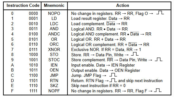
I build this on a breadboard using three resistor arrays because they are so easy to use on a breadboard and a Led Bar, also easy to use on a breadboard because it will save you a lot of wiring. You might say that the 330 ohm resistors between the dipswitch and the + 5V are not needed and you are right. But I put them there because on a breadboard a faulty wire may cause a shortage and by adding these resistors I save myself from destroying a line of the processor with a mistake of wiring. If you do this long enough you try to be careful.
Links and download
Motorola MC14500B processor

This page is about the Motorola MC14500B, a simple 1-bit microprocessor also called an Industrial Control Unit (ICU). The MC14500B is a CMOS one-bit microprocessor designed by Motorola in 1977 for simple control applications. I got to know this microprocessor through some open source projects and since the IC is still available it was a nice experiment to investigate. After a short time I got so excited about this little beast with its so simple but powerful (quirky) design that I decided to write a circuit and a complete IDE for it. The idea is to develop a kind of higher meta language for it, just for fun.

The MC14500B is well suited for the implementation of ladder logic, so it can be used as a replacement for (or as) a programmable logic controller. The processor supports 16 commands that all take 1 cycle and the chip operates at a frequency of up to 1 MHz. The chip has an internal RC clock where an external resistor determines the frequency, but it can also be controlled by an external clock. The MC14500B unit does not contain an internal program counter, but expects an external counter to be incremented on the rising edge of the clock, which places the new instruction from the rom onto the 4-bit opcode bus. The size of the program and the size of the ROM can therefore be as large as the designer wants.

The chip has a 1 bit ALU and one 1 bit internal register to perform logical operations. In addition, the chip has a number of output lines that can receive a high pulse through instructions and where external logic can be controlled. The only internal RR register is also available as an output via a pin. The lines are: RR – the logic state of the internet RR register, JMP – this pin will be equal high during the execution of a JMP instruction, RTN – this pin will be equal high during the execution of an RTN instruction, FLAG 0 – this pin will be the same high while executing a NOP0 (0x00) instruction and FLAG F – this pin will be the same high while executing a NOPF (0xff) instruction.
There is no support for JMP and RTN on the chip itself, this can be implemented in hardware by the designer of the circuit. In its simplest form, the JMP pin controls the reset of the program counter, so that a JMP instruction will always result in JMP 0000 and thus a simple program loop can be made. The other signal pins can also be used for your own interpretation and in this way you can give your own interpretation in hardware to the operation of the RTN signal (which has nothing to do with an RTN instruction), for example to control something or to activate a latch. The same is true for both the NOPO and the NOPF instruction. The designer of the circuit is given complete freedom to fill this in himself, which makes it a wonderful universally applicable design.

It is a 5V static processor that can even be manually clocked externally, which also makes debugging very easy. In the most elementary version, I connected an 8-bit dip switch and an 8-bit LED array to the chip on a breadboard and was able to execute instructions via the dip switch (which was also connected to the clock line) that became visible on the output LEDs. This allowed me to completely figure out and document the sequence and timing of signals.
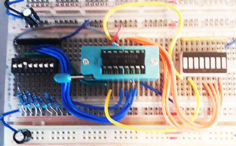
A nice open source project for the MC1400 is the PLC14500 from Nicola Cimmino (https://github.com/nicolacimmino/PLC-14500) this is a complete PLC solution using an MC14500 processor with 7 inputs, 7 outputs, an 8 bits sram and an adjustable timer that can be used under software control. The programming interface is very skimmed by means of an Arduino Nano that can take over the address and data bus from the program memory in order to upload new code. I am in contact with Nicola and have also ordered and built his board.

Being able to work with a microprocessor and a board also requires a programming environment. There were some separate programs, I converted my programming IDE for the MC14500 processor with a two pass assembler, a disassember, an emulator for various boards including visual display and clickable buttons, a single step debugger, breakpoint and trace capability. This IDE can also upload code directly into the various boards.
This IDE can be downloaded here at: https://www.heinpragt.nl/?product=mc14500b-processor-ide
This download is a zip file containing a portable x64 (and a x32 version) Windows exe programs, acustom bootloader and a examples directory.
Links and download
Information (old) microprocessors

I have been working in the computer industry since 1970 and I have used and programmed a lot of different microprocessors at work but also at home. I have been working as lead engineer of a R&D department for many years and I have designed a lot of equipment as embedded programmer and hardware designer. Nowedays it is sometimes hard to get an old microprocessor, sometimes you can still buy them. But a lot of old microprocessors and old computer support chips I get from disassembling old computer boards, but I lso buy them online and in East
European countries thay have a lot of old equipment and chips. Some microprocessors are special to me and they have their own page on this website. I also try to tell something about these processors and try to link to other information like wikipeadia and datasheets that I collect. The overview is organized according to the first year the microprocessor came out. There is also an overview of support chips (PIO.SIO,PIA,VIA,UART,DMA controllers) and and the video controller and sound controller chips. The year 1976 was a very successful year for new processors, this was the year that I became 17 years old and was very interested in home computers. This page is an overview of old computer chips. Kind regards, Hein Pragt.
| 1971 | |
| 1971 |
4004 (Processor)
|
| 1972 | |
| 1972 |
8008 (Processor)
|
| 1973 | |
| 1973 | |
| 1974 | |
| 1974 |
RCA 1802 (Processor)
MC6820 (Peripheral Interface Adapter)
Intel 8080 (Processor)
Intel 8224 (Clock generator)
Intel 8212 (Input/Output port)
Motorola 6800 (Processor)
|
| 1975 | |
| 1975 |
6502 (Processor)
650x (Processor)
R6532(RIOT)
AM2901CPC (4 Bits processor)
Signetics 2650 (8 Bits processor)
|
| 1976 | |
| 1976 |
Z80 (Processor)
z84c2006pec Z80 PIO
Z84C4006PEC Z80 SIO
Z8430 Z80 CTC
INS8060, of SC/MP (Processor)
Intel 8085 (Processor)
Intel MSC-49 FamilyNEC UPD8022C (Processor)
Intel 8035 (Processor)
Intel 8039 (Processor)
Intel 8039 (Processor)
8041 (UPI)
D8741 (UPI)
8042 (UPI)
8048 (MCU)
P8748 (MCU)
8049 (MCU)
8050 (8 bit Microsontroller)
MC6821 (Peripheral Interface Adapter)
TMS9900 (Processor)
P8274 (Intel – Multi Protocol Serial Controller)
P8253 (PROGRAMMABLE INTERVAL TIMER AMD)
D3242 (Multiplex / Refresh dram contr.)
|
| 1977 | |
| 1977 |
AM9080 (Processor)
6802 (Processor)
Motorola 6808 (Processor)
MC14500BCP (Processor)
MC6845 (Display controller)
6522 (Versatile Interface Adapter VIA)
P8155 (2048 bit sram – I/O port – timer)
P8243 (MS-48 I/O expander)
MK3870 (8-bit microcontroller)
|
| 1978 | |
| 1978 |
Motorola 6809 (Processor)
Motorola 6803 (Processor)
Motorola 6840 (Programmable Timer Module PTM)
Intel 8086 (Processor)
Intel 8087 (Floating-point Co-Processor)
AY-3-8910A (Sound)
SN76477N (Sound generator)
|
| 1979 | |
| 1979 |
Motorola 68000 (Processor)
Motorola 68901 (Multi-Function Peripheral)
Intel 8088 (Processor)
TMS9918 (Video controller)
TMS9118 (Video controller)
MC6847P (Video controller)
SAA5050 (Video controller)
SAA5051 (Teletext video controller) Philips)
Zilog Z8 (Processor)
P8256AH (Support Intel)
D8255AC (Support NEC)
D8259AC (Programmable Interrupt Controller NEC)
UPD765AC (Single/Double Density FDisk Controller NEC)
UPB8214 (PRIORITY INTERRUPT CONTROLLER NEC)
INS8243N (Iunput / output expander)
D8251AC (Prog. Comm. Interface)
AM2964 (Dynamic memory controller)
Intel D8089 (I/O Processor)
|
| 1980 | |
| 1980 |
Intel 8031 (Processor)
Intel 8051 (Processor)
Intel 8344 (Processor)
Intel 8044 (Processor)
Intel 8744 (Processor)
Intel 8051 (Processor)
Intel 8052 (Processor)
Intel 8751 (Processor)
SN76489AN (Sound generator)
P80C152 (UNIVERSAL COMMUNICATION CONTROLLER 8051)
P8237A (Intel DMA CONTROLLER)
MOS6561 (VIC video chip)
80A (Rusian Z80 clone)
D8293 (Bus Driver/Transceivers)
|
| 1981 | |
| 1981 |
TMS9914 (General bus adapter)
uPB8284AD (CLOCK GENERATOR AND DRIVER)
WD8250-PL (ACE)
|
| 1982 | |
| 1982 |
NEC 8086 (Processor)
Hitachi HD63B03 (Processor)
Hitachi HD63C09 (Processor)
Motorola MC68008P10 (Processor)
Motorola MC68010P12 (Processor)
Intel 80186 (Processor)
Intel 80286 (Processor)
Intel 80287 (Floating-point Co-Processor)
TMS9937 (Video Timers Controller)
MOS6510 (Processor)
D71059C (Interrupt controller)
P82586 (Ethernet chip)
AM29x305 (Processor)
|
| 1983 | |
| 1983 |
SCN68562 (DUSCC)
YM2149F (Sound)
MC68230 (Parallel Interface/Timer)
EM83050 (Keyboard controller PC)
MOS906114-01 (Commodore PLA chip)
UA6527 (Nes CPU clone 6502)
MH8228 (System Controller and Bus Driver for 8080A)
|
| 1984 | |
| 1984 |
Atmel AT89C2051 (Processor)
NEC V20 (Processor)
NEC V30 (Processor)
Motorola 68HC11 (Processor)
YM2203C (Sound generator)
HCS10017 (Oric Atmos ULA)
MOS8360R2 (TED chip comnodore 16)
MC2681P (Serial I/O Controller, 2 Channels)
MC68HC05C4 (6800) MCU
HD63484 (Graphics processor)
uPB8282C (8 bit Latches)
MC68701 (M6800 upgrade with Eeprom & RAM)
M50955 (Single chip computer based in 6502)
|
| 1985 | |
| 1985 |
HD614023S (Processor)
YM2608 (Sound chip)
YM3812 (OPL2 Sound chip)
MC68HC681 (DUART)
|
| 1986 | |
| 1986 |
AM33C93A (SCSI Controller)
P8052-Basic (MCU + Basic)
|
| 1987 | |
| 1987 |
TMP82C79P (Programmable keyboard / display interface)
D71054C (Programable Timer Counter)
|
| 1988 | |
| 1988 | |
| 1989 | |
| 1989 |
UB8002D (Rusian Z8002 clone)
|
| 1990 | |
| 1990 |
TMP47C432AP (Processor)
|
| 1991 | |
| 1991 | |
| 1992 | |
| 1992 |
TMS390 Sun SPARK processor
|
| 1993 | |
| 1993 | |
| 1994 | |
| 1994 |
COP888EG-DDU/N (Processor)
|
| 1995 | |
| 1995 | |
| 1996 | |
| 1996 | |
| 1997 | |
| 1997 |
Atmega328 (Processor)
Atmega32A (Processor)
|
| 1998 | |
| 1998 |
PIC16F876 and PIC16F877 (Processor)
|
| 1999 | |
| 1999 |
Attiny85 (Processor)
|
| 2000 and shortly after | |
| 2000 |
SH69P25K (4 bit microcontroller)
MC908QY4CPE (Processor)
XC68HC705DGP (Processor)
|
 In 1971 Intel created the first real microcessor chip the Intel 4004. It is a legendary chip amd not many are available nowadays.
 In 1972 Intel introduced their second real microcessor chip the Intel 8008. It is also a legendary chip amd not many are available nowadays.
 In 1974 the RCA 1802 (COSMAC 8-bit microprocessor family) became available, the processor design began in 1973. Most processors of that time were NMOS,
the 1802 was implemented in CMOS and used static logic. It did not have that much success for microcomputers and the company designed a (DIY) single board simple
computer called the COSMAC ELF, with switches to enter code and data and two hexadecimal LED displays. It was used as embedded controller especially aerospace and the
Hubble Space Telescope. The 1802 also ran the Galileo probe to Jupiter in 1989. Some computers were based on the 1802 like some ELF based systems, the
COMX-35 home computer and Telmac home computers in Finland only. The COMX-35 was the only computer that I knew and saw working. It is a funny but a little
strange processor.
In 1974 the RCA 1802 (COSMAC 8-bit microprocessor family) became available, the processor design began in 1973. Most processors of that time were NMOS,
the 1802 was implemented in CMOS and used static logic. It did not have that much success for microcomputers and the company designed a (DIY) single board simple
computer called the COSMAC ELF, with switches to enter code and data and two hexadecimal LED displays. It was used as embedded controller especially aerospace and the
Hubble Space Telescope. The 1802 also ran the Galileo probe to Jupiter in 1989. Some computers were based on the 1802 like some ELF based systems, the
COMX-35 home computer and Telmac home computers in Finland only. The COMX-35 was the only computer that I knew and saw working. It is a funny but a little
strange processor. In 1974, together with the MC6800 family Motorola introduced a PIA (Peripheral Interface Adapter) like the MC6820 as a 40 pin DIP chip to support the 6800
processor. It provided 20 I/O lines (two 8-bit bidirectional ports and 4 control lines for handshaking and interrupt generation. The MC6820 was used in the
Apple I to interface the ASCII keyboard and the display. It was also used in electronic pinball machines, the Atari 400 / Atari 800 and Commodore PET.
In 1974, together with the MC6800 family Motorola introduced a PIA (Peripheral Interface Adapter) like the MC6820 as a 40 pin DIP chip to support the 6800
processor. It provided 20 I/O lines (two 8-bit bidirectional ports and 4 control lines for handshaking and interrupt generation. The MC6820 was used in the
Apple I to interface the ASCII keyboard and the display. It was also used in electronic pinball machines, the Atari 400 / Atari 800 and Commodore PET.
 In 1974 Intel introduced the 8080 processor, and 8-bit microprocessor designed and manufactured by Intel and it was an extended and enhanced variant of the earlier
8008 design. The 8080 needs two support chips to function: the i8224 clock generator/driver and the i8228 bus controller. The first version was implemented in
NMOS and needed a +12 V and a −5 V and + 5 voltage. With its full 16-bit address bus it could access 64 KB of memory. It had a good competitor in the Z80, that
was binary compatible and had a lot of more instructions and registers. It was used in the Altair 8800 and S-100 bus personal computers and it was the base for
the CP/M operating system until the Z80 took over.
In 1974 Intel introduced the 8080 processor, and 8-bit microprocessor designed and manufactured by Intel and it was an extended and enhanced variant of the earlier
8008 design. The 8080 needs two support chips to function: the i8224 clock generator/driver and the i8228 bus controller. The first version was implemented in
NMOS and needed a +12 V and a −5 V and + 5 voltage. With its full 16-bit address bus it could access 64 KB of memory. It had a good competitor in the Z80, that
was binary compatible and had a lot of more instructions and registers. It was used in the Altair 8800 and S-100 bus personal computers and it was the base for
the CP/M operating system until the Z80 took over. In 1974 Intel produced some support chips for their 8080 processor and the 8224 chip was a single chip clock generator for the 8080 processor. It included circuits
to provide power-up reset, status strobe and sync of ready. It was mend to reduce the chip count of 8080 based computers.
In 1974 Intel produced some support chips for their 8080 processor and the 8224 chip was a single chip clock generator for the 8080 processor. It included circuits
to provide power-up reset, status strobe and sync of ready. It was mend to reduce the chip count of 8080 based computers. In 1974 Intel produced some support chips for their 8080 processor and the 8212 was an I/O chip designed for the Intel 8080/8085 processors. The device
comes in a 24-pin DIL package. Its main function is an 8-bit latch and an interrupt request flip-flop. It was mend to reduce the chip count of 8080 based
computers.
In 1974 Intel produced some support chips for their 8080 processor and the 8212 was an I/O chip designed for the Intel 8080/8085 processors. The device
comes in a 24-pin DIL package. Its main function is an 8-bit latch and an interrupt request flip-flop. It was mend to reduce the chip count of 8080 based
computers. In 1974 Motorola introduced the 6800 processor, it is an 8-bit microprocessor and one of the first that only needed a single 5V power supply. The 6800
has a 16-bit address bus that can directly access 64 KB of memory and an 8-bit bi-directional data bus. It has 72 instructions with seven addressing
modes for a total of 197 opcodes. The 6800 was popular in computer peripherals, test equipment applications and point-of-sale terminals. It also
found use in arcade games and pinball machines.
In 1974 Motorola introduced the 6800 processor, it is an 8-bit microprocessor and one of the first that only needed a single 5V power supply. The 6800
has a 16-bit address bus that can directly access 64 KB of memory and an 8-bit bi-directional data bus. It has 72 instructions with seven addressing
modes for a total of 197 opcodes. The 6800 was popular in computer peripherals, test equipment applications and point-of-sale terminals. It also
found use in arcade games and pinball machines.
 In 1975 MOS Technology introduced the 6502 8-bit microprocessor that was designed by a small team led by Chuck Peddle, a team that had formerly worked at Motorola
on the Motorola 6800 project. The 6502 is essentially a simplified, less expensive and faster version of the 6800 design. It was cheap and the biggest competitor
of the Z80 processor. I never used this processor, for me it was inferior to the Z80, with no I/O (only memory mapped I/O) and a very limited instruction set. But
the processor became very popular in systems like the Atari 2600, Atari 8-bit family, Apple II, Nintendo Entertainment System, Commodore 64, Atari Lynx, and the
BBC Microcomputer. Today the CMNOS version is still used in embedded systems. The difference between the 6502 and the 6502A is that the A version runs at 2 Mhz
and the normal 6502 version at 1Mhz.
I have two 40 pins DIL processors MOS6502 and UM6502A, but it is still not my favorite processor.
In 1975 MOS Technology introduced the 6502 8-bit microprocessor that was designed by a small team led by Chuck Peddle, a team that had formerly worked at Motorola
on the Motorola 6800 project. The 6502 is essentially a simplified, less expensive and faster version of the 6800 design. It was cheap and the biggest competitor
of the Z80 processor. I never used this processor, for me it was inferior to the Z80, with no I/O (only memory mapped I/O) and a very limited instruction set. But
the processor became very popular in systems like the Atari 2600, Atari 8-bit family, Apple II, Nintendo Entertainment System, Commodore 64, Atari Lynx, and the
BBC Microcomputer. Today the CMNOS version is still used in embedded systems. The difference between the 6502 and the 6502A is that the A version runs at 2 Mhz
and the normal 6502 version at 1Mhz.
I have two 40 pins DIL processors MOS6502 and UM6502A, but it is still not my favorite processor. In 1975 Rockwell introduced the R6532 (RIOT) Ram, I/O, Timer chip, that contained 128 x 8 bytes static ram, two 8 bit bidirectional data ports and a programmable timer
with interrupt capabilities. It was 6500 / 6800 bus compatible and I found the use of this chip in electronic pinball machines at that time and I know that the Atari 2600 used one.
In 1975 Rockwell introduced the R6532 (RIOT) Ram, I/O, Timer chip, that contained 128 x 8 bytes static ram, two 8 bit bidirectional data ports and a programmable timer
with interrupt capabilities. It was 6500 / 6800 bus compatible and I found the use of this chip in electronic pinball machines at that time and I know that the Atari 2600 used one.
 Am2900 is a family of integrated circuits (ICs) created in 1975 by Advanced Micro Devices (AMD). There is something special about this chip, the Am2900 family
was able to implement a CCU with data, addresses, and instructions to be any multiple of 4 bits by multiplying the number of ICs. The Am2901 chip was the
arithmetic-logic unit (ALU), and the “core” of the series. It could count using 4 bits and implement binary operations as well as various bit-shifting operations.
The 2901 and some other chips in the family were second sourced by an unusually large number of other manufacturers and was still in production in 2016.
Am2900 is a family of integrated circuits (ICs) created in 1975 by Advanced Micro Devices (AMD). There is something special about this chip, the Am2900 family
was able to implement a CCU with data, addresses, and instructions to be any multiple of 4 bits by multiplying the number of ICs. The Am2901 chip was the
arithmetic-logic unit (ALU), and the “core” of the series. It could count using 4 bits and implement binary operations as well as various bit-shifting operations.
The 2901 and some other chips in the family were second sourced by an unusually large number of other manufacturers and was still in production in 2016.
 The Signetics 2650 was introduced in July 1975 and it was an 8-bit microprocessor with a rather odd design. Because of the rather odd design and the
complex and odd memory access the processor was not used in commercial products that often. Actually the chip was designed in 1972 and the designer
selected the IBM 1130 as the model. But due to high chip production for Dolby the processor was only introduced in 1975. Advanced features were
status bits that were used to track the status of input/output devices and vectored interrupts. The 2650’s processor registers were divided into
two sets of three index registers, with a single global register R0 used as the accumulator. It had an odd address bus that was only 15 bits wide
and had some paging bits as well so only 8 KB could be addressed directly.
The Signetics 2650 was introduced in July 1975 and it was an 8-bit microprocessor with a rather odd design. Because of the rather odd design and the
complex and odd memory access the processor was not used in commercial products that often. Actually the chip was designed in 1972 and the designer
selected the IBM 1130 as the model. But due to high chip production for Dolby the processor was only introduced in 1975. Advanced features were
status bits that were used to track the status of input/output devices and vectored interrupts. The 2650’s processor registers were divided into
two sets of three index registers, with a single global register R0 used as the accumulator. It had an odd address bus that was only 15 bits wide
and had some paging bits as well so only 8 KB could be addressed directly.
 The Z80 (my first love as a processor) design started in 1974 when Federico Faggin left Intel to start the Zilog company with Ralph Ungermann. Faggin previously
worked as chief designer on, among others, the Intel 4004 and the 8080 processor. The Z80 is an 8 bit processor and officially released in 1976. The processor is
opcode compatible with Intel’s 8080 (which was a very slim move), but had more instructions, registers and addressing methods. The Z80 was designed for use in
computer terminals, printers, cash registers, but many home computers have also been produced based on the Z80 computer such as the TRS80, the Sinclair computer
series, the Philips P2000 and the well-known MSX computers. Even today there is still a club of avid hobbyists who build designs for the Z80 microprocessor.
The chip is still available. The Z80 processor was the main processor in my first TRS80 computer, the Sinclair ZX81, the Sinclair Spectrum, the MSX1 and MSX2
computer and the CP/M systems and embedded machine control units at my first job.
The Z80 (my first love as a processor) design started in 1974 when Federico Faggin left Intel to start the Zilog company with Ralph Ungermann. Faggin previously
worked as chief designer on, among others, the Intel 4004 and the 8080 processor. The Z80 is an 8 bit processor and officially released in 1976. The processor is
opcode compatible with Intel’s 8080 (which was a very slim move), but had more instructions, registers and addressing methods. The Z80 was designed for use in
computer terminals, printers, cash registers, but many home computers have also been produced based on the Z80 computer such as the TRS80, the Sinclair computer
series, the Philips P2000 and the well-known MSX computers. Even today there is still a club of avid hobbyists who build designs for the Z80 microprocessor.
The chip is still available. The Z80 processor was the main processor in my first TRS80 computer, the Sinclair ZX81, the Sinclair Spectrum, the MSX1 and MSX2
computer and the CP/M systems and embedded machine control units at my first job. This chip is basically just a digital parallel I/O port chip. You can configure the individual port pins as digital inputs or outputs and then use them for
whatever you want. The A/B input selects between either PortA or PortB and the C/D input selects between either the control register or the data register. The
control registers are used to configure the ports and the data registers are used to read/write the actual data. By connecting these to A0 and A1 one can access
the desired register using the address bus in an I/O read or write. The least significant bit of the memory address A0 then seledts the port A or B and the A1
line selects between the data and the control registers. With an address decoder you can put this chip anywhere in the I/O addressing space. In a lot of systems
this chip was used to add a parallel printer port to the Z80 system. But the chip can also handle digital inputs from switches and can be used to driver
signaling LEDs. One of the unique features of the Z80-PlO is that all data transfer between the peripheral device and the CPU can be accomplished
under total interrupt control even with nested interrupts. The the PlO can be programmed to interrupt if any specified peripheral alarm conditions
should occur. This interrupt capability reduces the amount of time that the processor has to spend in polling peripheral status.You can still buy
this chip and it costs only a few dollars.
This chip is basically just a digital parallel I/O port chip. You can configure the individual port pins as digital inputs or outputs and then use them for
whatever you want. The A/B input selects between either PortA or PortB and the C/D input selects between either the control register or the data register. The
control registers are used to configure the ports and the data registers are used to read/write the actual data. By connecting these to A0 and A1 one can access
the desired register using the address bus in an I/O read or write. The least significant bit of the memory address A0 then seledts the port A or B and the A1
line selects between the data and the control registers. With an address decoder you can put this chip anywhere in the I/O addressing space. In a lot of systems
this chip was used to add a parallel printer port to the Z80 system. But the chip can also handle digital inputs from switches and can be used to driver
signaling LEDs. One of the unique features of the Z80-PlO is that all data transfer between the peripheral device and the CPU can be accomplished
under total interrupt control even with nested interrupts. The the PlO can be programmed to interrupt if any specified peripheral alarm conditions
should occur. This interrupt capability reduces the amount of time that the processor has to spend in polling peripheral status.You can still buy
this chip and it costs only a few dollars. Together with the Z80 processor Zilog also produced some support chips and one of these chips was the Z80 SIO. It is basically a two channel serial input / output
device, with all control logic on board. Because a lot of Z80 systems were using a serial console for input and output, this was an important chip. It is a perfect
match with the Z80.
Together with the Z80 processor Zilog also produced some support chips and one of these chips was the Z80 SIO. It is basically a two channel serial input / output
device, with all control logic on board. Because a lot of Z80 systems were using a serial console for input and output, this was an important chip. It is a perfect
match with the Z80. Together with the Z80 processor Zilog also produced some support chips and one of these chips was the Z80 CTC. The Z80 CTC is a four-channel counter/timer that can be
programmed by system software for a broad range of counting and timing applications. These four independently programmable channels can be used for system event counting,
interrupt and interval timing, and clock rate generation.
Together with the Z80 processor Zilog also produced some support chips and one of these chips was the Z80 CTC. The Z80 CTC is a four-channel counter/timer that can be
programmed by system software for a broad range of counting and timing applications. These four independently programmable channels can be used for system event counting,
interrupt and interval timing, and clock rate generation. In 1976, National Semiconductor released the INS8060 or SC/MP (pronounced scamp) processor as a Simple Cost-effective Micro Processor. The processor had a few odd
quirks like a 12 bit program counter and four bank switch address bits on the data port and the odd ability to use one control pin to control three processors on
a single set of memory making it very easy to create a multiprocessor system. It also had to reduce costs a 1 bit ALU so the processor was not really fast. But
it was a nice simple design and the well-known electronics magazine Elektuur built several systems along. This was my first encounter with a microprocessor.
Sinclair released a board called MK14 with an SC/MP processor on it. In front of to the hobbyist it was a nice and relatively cheap processor, in the industry
it did not catch on. I bought one but at the last minute the buyer doubled the price, so I still do not have one.
In 1976, National Semiconductor released the INS8060 or SC/MP (pronounced scamp) processor as a Simple Cost-effective Micro Processor. The processor had a few odd
quirks like a 12 bit program counter and four bank switch address bits on the data port and the odd ability to use one control pin to control three processors on
a single set of memory making it very easy to create a multiprocessor system. It also had to reduce costs a 1 bit ALU so the processor was not really fast. But
it was a nice simple design and the well-known electronics magazine Elektuur built several systems along. This was my first encounter with a microprocessor.
Sinclair released a board called MK14 with an SC/MP processor on it. In front of to the hobbyist it was a nice and relatively cheap processor, in the industry
it did not catch on. I bought one but at the last minute the buyer doubled the price, so I still do not have one. In 1976 Intel introduced the 8085 8-bit microprocessor that was software-binary compatible with the Intel 8080 with only two minor instructions added. The 5 in
the part number was because the 8085 used only a single +5 V power supply, unlike the 8080 that required +5 V, −5 V and +12 V. The processor was a competitor
(Intel ‘s answer to) the very popular Z80 processor. The 8085 was often used as microcontroller in embedded systems thanks to its built-in serial I/O and
five prioritized interrupts, features that the Z80 CPU did not have. It was used in the famous VT102 terminal and the TRS-80 Model 100. The processor was
also cloned in the Soviet Union and also NASA used it in several space missions. I never used it, I was a Z80 fan.
In 1976 Intel introduced the 8085 8-bit microprocessor that was software-binary compatible with the Intel 8080 with only two minor instructions added. The 5 in
the part number was because the 8085 used only a single +5 V power supply, unlike the 8080 that required +5 V, −5 V and +12 V. The processor was a competitor
(Intel ‘s answer to) the very popular Z80 processor. The 8085 was often used as microcontroller in embedded systems thanks to its built-in serial I/O and
five prioritized interrupts, features that the Z80 CPU did not have. It was used in the famous VT102 terminal and the TRS-80 Model 100. The processor was
also cloned in the Soviet Union and also NASA used it in several space missions. I never used it, I was a Z80 fan.
 In 1974, together with the MC6800 family Motorola introduced a PIA (Peripheral Interface Adapter) like the MC6820 as a 40 pin DIP chip to support
the 6800 processor. It provided 20 I/O lines (two 8-bit bidirectional ports and 4 control lines for handshaking and interrupt generation. In 1976 Motorola
switched the MC6800 family to a depletion-mode technology so the MC6820 became the MC6821. The MC6820 was used in the Apple I to interface the ASCII keyboard
and the display. The Tandy Color Computer used two MC6821s to provide I/O access to the video, audio and peripherals.
In 1974, together with the MC6800 family Motorola introduced a PIA (Peripheral Interface Adapter) like the MC6820 as a 40 pin DIP chip to support
the 6800 processor. It provided 20 I/O lines (two 8-bit bidirectional ports and 4 control lines for handshaking and interrupt generation. In 1976 Motorola
switched the MC6800 family to a depletion-mode technology so the MC6820 became the MC6821. The MC6820 was used in the Apple I to interface the ASCII keyboard
and the display. The Tandy Color Computer used two MC6821s to provide I/O access to the video, audio and peripherals.
 In June 1976 Texas Instruments introduced the TMS9900 processor and it was one of the first commercially available, single-chip 16-bit microprocessors. It
implemented Texas Instruments’ TI-990 minicomputer architecture in a single-chip but the 64-pin DIP format made it more expensive to implement in smaller
machines than the more common 40-pin DIP chips. It was used in the Texas Instruments own home computer the TI-99/4. It has a little strange architecture
compared to other microprocessors of that time, given its origin from a mini-computer.
In June 1976 Texas Instruments introduced the TMS9900 processor and it was one of the first commercially available, single-chip 16-bit microprocessors. It
implemented Texas Instruments’ TI-990 minicomputer architecture in a single-chip but the 64-pin DIP format made it more expensive to implement in smaller
machines than the more common 40-pin DIP chips. It was used in the Texas Instruments own home computer the TI-99/4. It has a little strange architecture
compared to other microprocessors of that time, given its origin from a mini-computer. In 1976 (as far as I know) Intel introduced the P8274 Multi Protocol Serial Controller. It had two independent full duplex transmitters and receivers,
it could do asynchronous, Byte synchronous and Bit synchronous operation and was fully compatible with the 8048, 8051, 8085, 8088, 8086 CPU’s.
It supported 4 independent DMA channels.
In 1976 (as far as I know) Intel introduced the P8274 Multi Protocol Serial Controller. It had two independent full duplex transmitters and receivers,
it could do asynchronous, Byte synchronous and Bit synchronous operation and was fully compatible with the 8048, 8051, 8085, 8088, 8086 CPU’s.
It supported 4 independent DMA channels.
 In 1976 AMD introduced the P8253 Programmeble Interval Timer chipas as a licensed Intel second source. The P8253 is a programmable interval timer/counter
specially designed for Intel processors that can be treated as a series of I/O ports for access.
In 1976 AMD introduced the P8253 Programmeble Interval Timer chipas as a licensed Intel second source. The P8253 is a programmable interval timer/counter
specially designed for Intel processors that can be treated as a series of I/O ports for access.
 The Intel 3242 is an address multiplexer and refresh counter for multiplexed address dynamic rams. The chip a 7-bit refresh counter that is
externally controlled so it can support distributed and burst refresh. It is often used together with 2116 dram chips.
The Intel 3242 is an address multiplexer and refresh counter for multiplexed address dynamic rams. The chip a 7-bit refresh counter that is
externally controlled so it can support distributed and burst refresh. It is often used together with 2116 dram chips.
 In 1977 AMD reverse engineered the Intel 8080 processor and created the Am9080 a chip that could replace the 8080 chip. It was
originally produced without license but later an agreement was made with Intel to become a licensed second source for the 8080.
It is not a very common chip to find.
In 1977 AMD reverse engineered the Intel 8080 processor and created the Am9080 a chip that could replace the 8080 chip. It was
originally produced without license but later an agreement was made with Intel to become a licensed second source for the 8080.
It is not a very common chip to find.
 In 1977 Motorola introduced the 6802 processor based on the already famous 6800 design. It was a 8-bit microprocessor and it had a 16-bit address bus that
could directly access 64 KB of memory. The 6800 processor has 72 instructions with seven addressing modes for a total of 197 opcodes. The MC6802 included
128 bytes of RAM and an internal clock oscillator on chip.
In 1977 Motorola introduced the 6802 processor based on the already famous 6800 design. It was a 8-bit microprocessor and it had a 16-bit address bus that
could directly access 64 KB of memory. The 6800 processor has 72 instructions with seven addressing modes for a total of 197 opcodes. The MC6802 included
128 bytes of RAM and an internal clock oscillator on chip.
 In 1977 Motorola introduced the MC14500B (ICU) to replace relay systems and programmable logic controllers and serial data manipulation. The processor supports
16 commands and is operating at a frequency of 1 MHz. It does not have a program counter (PC), instead, a clock signal drives a separate chip that also determines
the supported memory size. The ICU architecture seems to be similar to that of the DEC PDP-14 computer.
In 1977 Motorola introduced the MC14500B (ICU) to replace relay systems and programmable logic controllers and serial data manipulation. The processor supports
16 commands and is operating at a frequency of 1 MHz. It does not have a program counter (PC), instead, a clock signal drives a separate chip that also determines
the supported memory size. The ICU architecture seems to be similar to that of the DEC PDP-14 computer. In 1977 Motorola introduced the MC6845 Display controller and it was widely used in 8-bit computers during the 1980s. It was originally designed for
the Motorola 6800 CPU but used for many more processors like the Zilog Z80 and MOS 6502. It was not a one in all solution, it needed other chips to
function and the implementation of that hardware is entirely up to the designer. It was used in the BBC Micro, Amstrad CPC, and Videx VideoTerm display
cards for the Apple II. It was also used in early graphics adapter cards for the IBM PC like the MDA, Hercules Graphics Card and Color Graphics Adapter (CGA).
In 1977 Motorola introduced the MC6845 Display controller and it was widely used in 8-bit computers during the 1980s. It was originally designed for
the Motorola 6800 CPU but used for many more processors like the Zilog Z80 and MOS 6502. It was not a one in all solution, it needed other chips to
function and the implementation of that hardware is entirely up to the designer. It was used in the BBC Micro, Amstrad CPC, and Videx VideoTerm display
cards for the Apple II. It was also used in early graphics adapter cards for the IBM PC like the MDA, Hercules Graphics Card and Color Graphics Adapter (CGA). In 1977 MOS Technology introduced the 6522 Versatile Interface Adapter (VIA), as an I/O port controller for the 6502 family of microprocessors. It provided two
bidirectional 8-bit parallel I/O ports, two 16-bit timers and an 8-bit shift register for serial communications. The 6522 was widely used in computers of the
1980s, particularly Commodore’s machines, the Apple III, Oric-1 and Oric Atmos, BBC Micro, Victor 9000 / Sirius 1, the Apple Macintosh and the Vectrex game console.
In 1977 MOS Technology introduced the 6522 Versatile Interface Adapter (VIA), as an I/O port controller for the 6502 family of microprocessors. It provided two
bidirectional 8-bit parallel I/O ports, two 16-bit timers and an 8-bit shift register for serial communications. The 6522 was widely used in computers of the
1980s, particularly Commodore’s machines, the Apple III, Oric-1 and Oric Atmos, BBC Micro, Victor 9000 / Sirius 1, the Apple Macintosh and the Vectrex game console.
 In 1977 Intel introduced the P8155 as support chip for the 8085 (and 8088) processor. It contains 2038 bits (256 x 8 bytes) static Ram, two programmeble 8 bit I/O
ports and one 6 bit programmeble I/O port and a 14 bit programmeble timer / counter. It was an attempt of Intel to lower the chip count in 8085 and 8088 designs.
In 1977 Intel introduced the P8155 as support chip for the 8085 (and 8088) processor. It contains 2038 bits (256 x 8 bytes) static Ram, two programmeble 8 bit I/O
ports and one 6 bit programmeble I/O port and a 14 bit programmeble timer / counter. It was an attempt of Intel to lower the chip count in 8085 and 8088 designs. The Intel 8243 contains four 4-bit I/O ports which serve as an extension to the on-chip I/O and are addressed as port 4 to 7. This chip is specially
designed for the 8048 processor and supports transfer from accumulator to port, port to accumulator, AND accumulator to port and OR accumulator to port.
The Intel 8243 contains four 4-bit I/O ports which serve as an extension to the on-chip I/O and are addressed as port 4 to 7. This chip is specially
designed for the 8048 processor and supports transfer from accumulator to port, port to accumulator, AND accumulator to port and OR accumulator to port. The MK3870 is an 8-bit microcontroller and a single chip implementation of Fairchild F8. The microcontroller includes up to 4 KB mask-programmable ROM, 64 bytes
scratchpad RAM and up to 64 bytes executable RAM. The MCU also integrates 32-bit I/O and programmable timer. There was also a MK38P70 development version of
the 3870 MCU that supported external EPROM chip. It was used in the Heathkit Aircraft Navigation Computer OCW-1401 that was basically a special calculator.
The MK3870 is an 8-bit microcontroller and a single chip implementation of Fairchild F8. The microcontroller includes up to 4 KB mask-programmable ROM, 64 bytes
scratchpad RAM and up to 64 bytes executable RAM. The MCU also integrates 32-bit I/O and programmable timer. There was also a MK38P70 development version of
the 3870 MCU that supported external EPROM chip. It was used in the Heathkit Aircraft Navigation Computer OCW-1401 that was basically a special calculator. In 1978 Motorola introduced the 6809, an 8-bit microprocessor with some 16-bit features. It was source compatible with Motorola 6800 but offered some good improvements.
Compared to other popular processors of that time it was very expensive (4 times the price of a Z80). It was used in the TRS-80 Color Computer, Dragon 32/64, SuperPET,
the famous Vectrex game console, and some arcade machines. I have never programmed this processor, but it is nice to have one.
In 1978 Motorola introduced the 6809, an 8-bit microprocessor with some 16-bit features. It was source compatible with Motorola 6800 but offered some good improvements.
Compared to other popular processors of that time it was very expensive (4 times the price of a Z80). It was used in the TRS-80 Color Computer, Dragon 32/64, SuperPET,
the famous Vectrex game console, and some arcade machines. I have never programmed this processor, but it is nice to have one. In 1978 Motorola also introduced the 6803, an 8-bit microprocessor with some 16-bit features. It was source compatible with Motorola 6800 but offered some good
improvements like the 6801 and 6802. The MC6803 had no ROM and fewer different bus configurations. I have never programmed this processor, but it is nice to have one.
In 1978 Motorola also introduced the 6803, an 8-bit microprocessor with some 16-bit features. It was source compatible with Motorola 6800 but offered some good
improvements like the 6801 and 6802. The MC6803 had no ROM and fewer different bus configurations. I have never programmed this processor, but it is nice to have one. In 1978 Motorola also introduced the 6840, the MC6840 programmable counter had three 16-bit binary counters that could be used for frequency measurement,
event counting, or interval measurement.
In 1978 Motorola also introduced the 6840, the MC6840 programmable counter had three 16-bit binary counters that could be used for frequency measurement,
event counting, or interval measurement. In 1978 Intel released the 8086 processor, the 8086 was also called iAPX 86 and it is a 16-bit microprocessor. The 8086 was the base
of all x86 architecture that became Intel’s most successful line of processors. I used this processor a lot and the segment registers that Intel used
in the 8086 CPU’s to access one megabyte of memory was a “pain in the ass” for many programmers. I used to replace the Intel processors
by the NEC version.
In 1978 Intel released the 8086 processor, the 8086 was also called iAPX 86 and it is a 16-bit microprocessor. The 8086 was the base
of all x86 architecture that became Intel’s most successful line of processors. I used this processor a lot and the segment registers that Intel used
in the 8086 CPU’s to access one megabyte of memory was a “pain in the ass” for many programmers. I used to replace the Intel processors
by the NEC version. In 1978 Intel also introduced the 8087 Floating-point Co-Processor, it is the math coprocessor for the Intel 8086 series of microprocessors. The popularity
of the 8087 got a real boost when IBM included a coprocessor socket on the IBM PC motherboard. The development of the 8087 led to the IEEE 754-1985 standard
for floating-point arithmetic.
In 1978 Intel also introduced the 8087 Floating-point Co-Processor, it is the math coprocessor for the Intel 8086 series of microprocessors. The popularity
of the 8087 got a real boost when IBM included a coprocessor socket on the IBM PC motherboard. The development of the 8087 led to the IEEE 754-1985 standard
for floating-point arithmetic.  In 1978 by General Instrument introduced the AY-3-8910 sound chip. It is a 3-voice programmable sound generator (PSG). The AY-3-8910 and its variants were
used in many arcade games and pinball machines but it was also the typical sound chip in the Intellivision and Vectrex video game consoles, the Amstrad CPC,
Oric-1, Colour Genie, MSX, and later ZX Spectrum home computers. It was also used in the Mockingboard and Cricket sound cards for the Apple II and the
Speech / Sound Cartridge for the TRS-80 Color Computer. After General Instrument’s spinoff of Microchip Technology in 1987, the chip was sold for a few years
under the Microchip brand. It was also manufactured under license by Yamaha as the YM2149F, the Atari ST uses this version.
In 1978 by General Instrument introduced the AY-3-8910 sound chip. It is a 3-voice programmable sound generator (PSG). The AY-3-8910 and its variants were
used in many arcade games and pinball machines but it was also the typical sound chip in the Intellivision and Vectrex video game consoles, the Amstrad CPC,
Oric-1, Colour Genie, MSX, and later ZX Spectrum home computers. It was also used in the Mockingboard and Cricket sound cards for the Apple II and the
Speech / Sound Cartridge for the TRS-80 Color Computer. After General Instrument’s spinoff of Microchip Technology in 1987, the chip was sold for a few years
under the Microchip brand. It was also manufactured under license by Yamaha as the YM2149F, the Atari ST uses this version.  In 1978 Texas Instruments introduced the SN76477 complex sound generator. The chip is typically used as a sound effects generator in arcade games
and toys. The use of the SN76477 in a musical context is limited by the fact that it was difficult to electronically control the pitch of the
produced sound. The SN76477 generates complex audio combining the outputs of a LFO, VCO and noise generator, through an envelope ADSR. The sound
generation is controlled by supplying control voltages, logic levels and different resistor and capacitor values.
In 1978 Texas Instruments introduced the SN76477 complex sound generator. The chip is typically used as a sound effects generator in arcade games
and toys. The use of the SN76477 in a musical context is limited by the fact that it was difficult to electronically control the pitch of the
produced sound. The SN76477 generates complex audio combining the outputs of a LFO, VCO and noise generator, through an envelope ADSR. The sound
generation is controlled by supplying control voltages, logic levels and different resistor and capacitor values. In 1979 Motorola introduced the 68000 processor, a 16/32-bit complex instruction set computer (CISC) microprocessor. It has a 32-bit instruction set, 32-bit registers
and a 16-bit internal data bus, the address bus is 24 bits and it uses a 16-bit ALU. The processor was used in a few high end computers like the Macintosh, Amiga and
Atari ST, and the Mega Drive console. All of these were known because of their great graphic capabilities. These system were too expensive for me at the time and so
I have never programmed a 68000 processor, but I have one MC68000P12 processor. Nowadays the 68000 architecture is still in use.
In 1979 Motorola introduced the 68000 processor, a 16/32-bit complex instruction set computer (CISC) microprocessor. It has a 32-bit instruction set, 32-bit registers
and a 16-bit internal data bus, the address bus is 24 bits and it uses a 16-bit ALU. The processor was used in a few high end computers like the Macintosh, Amiga and
Atari ST, and the Mega Drive console. All of these were known because of their great graphic capabilities. These system were too expensive for me at the time and so
I have never programmed a 68000 processor, but I have one MC68000P12 processor. Nowadays the 68000 architecture is still in use. Intel introduced the Intel 8088 on June 1, 1979, the processor has an eight-bit external data bus instead of the 16-bit bus of the 8086. The 16-bit registers
and the one megabyte address range are unchanged, it was intended to be a version of the 8086 for cheaper system. The original IBM PC used the 8088 at a clock
frequency of 4.77 MHz. Some of IBM’s engineers wanted another (better) processor but Intel offered the best price. This processor was the beginning of the whole
x86 processor range of Intel.
Intel introduced the Intel 8088 on June 1, 1979, the processor has an eight-bit external data bus instead of the 16-bit bus of the 8086. The 16-bit registers
and the one megabyte address range are unchanged, it was intended to be a version of the 8086 for cheaper system. The original IBM PC used the 8088 at a clock
frequency of 4.77 MHz. Some of IBM’s engineers wanted another (better) processor but Intel offered the best price. This processor was the beginning of the whole
x86 processor range of Intel. In 1979 Texas Instruments introduced the TMS9918 video display controller (VDC). This is a famous video processor that was used in a lot of systems like the
ColecoVision, CreatiVision, Memotech MTX, MSX, SG-1000/SC-3000, Spectravideo, Sord M5, Sega game gear, Texas Instruments TI-99/4 and the Casio PV-2000. The TMS9918
generates both grid-based character graphics (used to display text or background images) and sprites used for moving foreground objects. I have used this
processor and programmed it in my first MSX-1 computer. The TMS9928 and TMS9929 are variants of the TMS9918.
In 1979 Texas Instruments introduced the TMS9918 video display controller (VDC). This is a famous video processor that was used in a lot of systems like the
ColecoVision, CreatiVision, Memotech MTX, MSX, SG-1000/SC-3000, Spectravideo, Sord M5, Sega game gear, Texas Instruments TI-99/4 and the Casio PV-2000. The TMS9918
generates both grid-based character graphics (used to display text or background images) and sprites used for moving foreground objects. I have used this
processor and programmed it in my first MSX-1 computer. The TMS9928 and TMS9929 are variants of the TMS9918.  In 1979 Texas Instruments also introduced the TMS9118 video display controller (VDC). This is a lesser used famous video processor that was used in some MSX-1 computers.
The TMS9118 is a variant of the TMS9918 with a different external ram configuration of 16K x 4 ram chips.
In 1979 Texas Instruments also introduced the TMS9118 video display controller (VDC). This is a lesser used famous video processor that was used in some MSX-1 computers.
The TMS9118 is a variant of the TMS9918 with a different external ram configuration of 16K x 4 ram chips.
 In 1979 Motorola introduced the MC6847P video display controller (VDC). It was used in the TRS-80 Color Computer, Dragon 32/64, Laser 200, TRS-80 MC-10,
NEC PC-6000 series, Acorn Atom, and it is a relatively simple display generator compared to other display chips of the time. It is capable of displaying
text and graphics contained within a roughly square display matrix 256 pixels wide by 192 lines high. The ROM includes a 5 x 7 pixel font, compatible
with 6-bit ASCII. Effects such as inverse video or colored text are possible. It is capable of displaying nine colors. The low display resolution was
a necessity of using television sets as display monitors.
In 1979 Motorola introduced the MC6847P video display controller (VDC). It was used in the TRS-80 Color Computer, Dragon 32/64, Laser 200, TRS-80 MC-10,
NEC PC-6000 series, Acorn Atom, and it is a relatively simple display generator compared to other display chips of the time. It is capable of displaying
text and graphics contained within a roughly square display matrix 256 pixels wide by 192 lines high. The ROM includes a 5 x 7 pixel font, compatible
with 6-bit ASCII. Effects such as inverse video or colored text are possible. It is capable of displaying nine colors. The low display resolution was
a necessity of using television sets as display monitors.  In 1979 Mullard introduced the SAA5050, a character generator chip for implementing the Teletext character set. The SAA5050 was used in teletext-equipped
television sets, viewdata terminals, and microcomputers like the Philips P2000, Acorn System 2 and BBC Microcomputer. The chip generated appropriate
video output for a 7-bit input character code representing the current character on the text line, full-screen resolution generated by the SAA5050
was 480×500 pixels, corresponding to 40×25 characters.
In 1979 Mullard introduced the SAA5050, a character generator chip for implementing the Teletext character set. The SAA5050 was used in teletext-equipped
television sets, viewdata terminals, and microcomputers like the Philips P2000, Acorn System 2 and BBC Microcomputer. The chip generated appropriate
video output for a 7-bit input character code representing the current character on the text line, full-screen resolution generated by the SAA5050
was 480×500 pixels, corresponding to 40×25 characters. The SAA5051 is also a character generator chip for implementing the Teletext character set, with a German characterset. The SAA5051 was used in teletext-equipped
television sets, viewdata terminals, and microcomputers. The chip generated appropriate video output for a 7-bit input character code representing the current
character on the text line, full-screen resolution generated by the SAA5051 was 480×500 pixels, corresponding to 40×25 characters.
The SAA5051 is also a character generator chip for implementing the Teletext character set, with a German characterset. The SAA5051 was used in teletext-equipped
television sets, viewdata terminals, and microcomputers. The chip generated appropriate video output for a 7-bit input character code representing the current
character on the text line, full-screen resolution generated by the SAA5051 was 480×500 pixels, corresponding to 40×25 characters.
 In 1979 Zilog introduced the Z8 microcontroller architecture. One of the features is up to 4,096 fast on-chip registers which may be used as accumulators, pointers
or as ordinary random-access memory (RAM). A 16-bit address space for between 1 kB and 64 kB of either PROM, ROM or flash memory and there is even a second 16-bit
address space. On chip peripherals include analog-to-digital converter, Serial Peripheral Interface (SPI) bus and I²C channels, IrDA encoders / decoders etc.
There are versions with from 8 up to 80 pins and a lot of different packages.
In 1979 Zilog introduced the Z8 microcontroller architecture. One of the features is up to 4,096 fast on-chip registers which may be used as accumulators, pointers
or as ordinary random-access memory (RAM). A 16-bit address space for between 1 kB and 64 kB of either PROM, ROM or flash memory and there is even a second 16-bit
address space. On chip peripherals include analog-to-digital converter, Serial Peripheral Interface (SPI) bus and I²C channels, IrDA encoders / decoders etc.
There are versions with from 8 up to 80 pins and a lot of different packages. This chip is an Intel Multifunction microprocessor support controller with a SIO (Serial interface) and PIO (Parallel interface), timers and an Interrupt controller
all in one chip. I do not know the year it cam out and I never used one but I have calculated it came ouit around 1979.
This chip is an Intel Multifunction microprocessor support controller with a SIO (Serial interface) and PIO (Parallel interface), timers and an Interrupt controller
all in one chip. I do not know the year it cam out and I never used one but I have calculated it came ouit around 1979.  This chip is a PIO ( parallel Input Output) device from NEC with 24 programmable I/O lines. It can be used in the same way as an Z80 PIO. I do not know
the year it cam out and I never used one but I have calculated it came ouit around 1979. NEC produced all Intel chips as second source under licence since 1976.
This chip is a PIO ( parallel Input Output) device from NEC with 24 programmable I/O lines. It can be used in the same way as an Z80 PIO. I do not know
the year it cam out and I never used one but I have calculated it came ouit around 1979. NEC produced all Intel chips as second source under licence since 1976.
 The 8259 is a Programmable Interrupt Controller (PIC) designed for the Intel 8085 and Intel 8086 microprocessors. The 8259 combines multiple interrupt input sources
to a single interrupt output to the host microprocessor, expanding the interrupt levels available in a system.
The 8259A was the interrupt controller for the ISA bus in the IBM PC and IBM PC AT and IBM also used the NEC chips for this.
NEC produced all Intel chips as second source under licence since 1976.
The 8259 is a Programmable Interrupt Controller (PIC) designed for the Intel 8085 and Intel 8086 microprocessors. The 8259 combines multiple interrupt input sources
to a single interrupt output to the host microprocessor, expanding the interrupt levels available in a system.
The 8259A was the interrupt controller for the ISA bus in the IBM PC and IBM PC AT and IBM also used the NEC chips for this.
NEC produced all Intel chips as second source under licence since 1976.
 The uPD765AC from NEC is a an LSI floppy disk controller (FDC) chip which contains the circuitry and control functions for interfacing a processor to 4 floppy
disk drives. . It is capableof either IBM 3740 singledensity format (FM), or IBM System 34 double density format (MFM) including double-sided recording.
The uPD765AC from NEC is a an LSI floppy disk controller (FDC) chip which contains the circuitry and control functions for interfacing a processor to 4 floppy
disk drives. . It is capableof either IBM 3740 singledensity format (FM), or IBM System 34 double density format (MFM) including double-sided recording.
 The UPB8214 from NEC is an eight-level priority interrupt controller, designed to simplify interrupt driven microcomputer systems. The interrupt structure
of the microcomputer system can be expanded beyond eight interrupt levels by cascading UPB8214s.
The UPB8214 from NEC is an eight-level priority interrupt controller, designed to simplify interrupt driven microcomputer systems. The interrupt structure
of the microcomputer system can be expanded beyond eight interrupt levels by cascading UPB8214s.
 The INS8243 is a n I/O expander specially designed for the INS8048 / INS8049 and INS8050 processors. It consists of five, four bit bidirectional
I/O ports in a 24 DIP package.
The INS8243 is a n I/O expander specially designed for the INS8048 / INS8049 and INS8050 processors. It consists of five, four bit bidirectional
I/O ports in a 24 DIP package.  The Intel 8251 is a standard Universal Synchronous/Asynchronous Receiver/Transmitter (USART) designed for the MCS-48, 8080, 8085, 8086 and 8088 processors.
NEC produced all Intel chips as second source under licence.
The Intel 8251 is a standard Universal Synchronous/Asynchronous Receiver/Transmitter (USART) designed for the MCS-48, 8080, 8085, 8086 and 8088 processors.
NEC produced all Intel chips as second source under licence.
 The AM2964 from AMD is a Dynamic Memory Controller (DMC), it has two 8 bit latches to hold the memory addresses. It also has a refresh counter to update
the refresh of the 16K or 64K dynamic rams.
The AM2964 from AMD is a Dynamic Memory Controller (DMC), it has two 8 bit latches to hold the memory addresses. It also has a refresh counter to update
the refresh of the 16K or 64K dynamic rams.
 The Intel 8089 is a microprocessor dedicated for inpu/outpu processing. It is made for the 8088 and 8086 processors and the chip performs
the function of an inteliogent DMA controller for the Intel iAPX 86 family. It can operate completely parallel with the CPU giving dramaticly
improved I/O performance. The chip has two I/O channels supporting a transferrate up to 1.25 mbyte/sec. It is not a very common chip.
The Intel 8089 is a microprocessor dedicated for inpu/outpu processing. It is made for the 8088 and 8086 processors and the chip performs
the function of an inteliogent DMA controller for the Intel iAPX 86 family. It can operate completely parallel with the CPU giving dramaticly
improved I/O performance. The chip has two I/O channels supporting a transferrate up to 1.25 mbyte/sec. It is not a very common chip. In 1980 Intel released the 8031 (family of the 8051) microcontroller and I have have used this one in my first modem design with and external eprom. The 8031 is just like
the 8051 an eight bit CISC processor. The 8031 had no rom and only 128 bytes ram on board which was a big challenge for the programmer. By default, the processor had a
number of Timers multiple interrupt lines and an internal serial uart on board and many programmable I/O pins. The processor wasn’t expensive and was used as a central
processor in many devices. Even today this processor is still used and it still is available.
I have several types of this processor like original Intel P8031, a SAB8031 (Siemens) and P80C321 (AMD)
In 1980 Intel released the 8031 (family of the 8051) microcontroller and I have have used this one in my first modem design with and external eprom. The 8031 is just like
the 8051 an eight bit CISC processor. The 8031 had no rom and only 128 bytes ram on board which was a big challenge for the programmer. By default, the processor had a
number of Timers multiple interrupt lines and an internal serial uart on board and many programmable I/O pins. The processor wasn’t expensive and was used as a central
processor in many devices. Even today this processor is still used and it still is available.
I have several types of this processor like original Intel P8031, a SAB8031 (Siemens) and P80C321 (AMD) In 1980 Intel released the 8051 microcontroller and I have designed many circuits and devices (modems) with this processor myself. The 8051 is an eight bit CISC processor
that has been marketed in many types, also by many other manufacturers of which Atmel is the is best known. The system normally had 4 kb rom and 256 bytes ram on board
which was a big challenge for the programmer. But there could also 64 kb of ROM and 64 kb of RAM can be connected externally, sacrificing many I/O pins. By default, the
processor had a number of Timers multiple interrupt lines and an internal serial uart on board and many programmable I/O pins. The processor wasn’t expensive either
and was used as a central processor in many devices. Even today this processor is still used and it still is available.
In 1980 Intel released the 8051 microcontroller and I have designed many circuits and devices (modems) with this processor myself. The 8051 is an eight bit CISC processor
that has been marketed in many types, also by many other manufacturers of which Atmel is the is best known. The system normally had 4 kb rom and 256 bytes ram on board
which was a big challenge for the programmer. But there could also 64 kb of ROM and 64 kb of RAM can be connected externally, sacrificing many I/O pins. By default, the
processor had a number of Timers multiple interrupt lines and an internal serial uart on board and many programmable I/O pins. The processor wasn’t expensive either
and was used as a central processor in many devices. Even today this processor is still used and it still is available. In 1980 Intel released the P8344AH, another variant of the 8051 microcontroller The 8051 is an eight bit CISC processor
that has been marketed in many types, also by many other manufacturers of which Atmel is the is best known. This chip has 4 kb rom and 192 bytes ram on board
which is a big challenge for the programmer. But there could also 64 kb of ROM and 64 kb of RAM can be connected externally, sacrificing many I/O pins. By default, the
processor had a number of Timers multiple interrupt lines and an internal serial uart on board and many programmable I/O pins. The processor wasn’t expensive either
and was used as a central processor in many devices.
In 1980 Intel released the P8344AH, another variant of the 8051 microcontroller The 8051 is an eight bit CISC processor
that has been marketed in many types, also by many other manufacturers of which Atmel is the is best known. This chip has 4 kb rom and 192 bytes ram on board
which is a big challenge for the programmer. But there could also 64 kb of ROM and 64 kb of RAM can be connected externally, sacrificing many I/O pins. By default, the
processor had a number of Timers multiple interrupt lines and an internal serial uart on board and many programmable I/O pins. The processor wasn’t expensive either
and was used as a central processor in many devices. The Intel P8044 is the same as the P8344, but has on chip 4Kb factory masked rom on board.
 The Intel C8744 is the same as the P8344, but has on chip 4Kb Programmable/UV Erasable EPROM on board and with on-chip serial
communication controller for SDLC/HDLC.
The Intel C8744 is the same as the P8344, but has on chip 4Kb Programmable/UV Erasable EPROM on board and with on-chip serial
communication controller for SDLC/HDLC. The 8051 is the basic bare 8-bit CPU from Intel, it has 8-bit registers (one 16-bit register with special move instructions),
8-bit data bus and 2×16-bit address buses, program counter, data pointer. Four fast switchable register banks with eight registers memory mapped),
fast interrupt with optional register bank switching and selectable priority, 128 bytes of on-chip RAM (IRAM), three full) 8-bit bi-directional
input/output ports, bit addressable UART (serial port) and two 16-bit counter/timers. It is indeed a MCU chip.
The 8051 is the basic bare 8-bit CPU from Intel, it has 8-bit registers (one 16-bit register with special move instructions),
8-bit data bus and 2×16-bit address buses, program counter, data pointer. Four fast switchable register banks with eight registers memory mapped),
fast interrupt with optional register bank switching and selectable priority, 128 bytes of on-chip RAM (IRAM), three full) 8-bit bi-directional
input/output ports, bit addressable UART (serial port) and two 16-bit counter/timers. It is indeed a MCU chip. The 8052 is the basic bare 8-bit CPU from Intel, it has 8-bit registers (one 16-bit register with special move instructions),
8-bit data bus and 2×16-bit address buses, program counter, data pointer. Four fast switchable register banks with eight registers memory mapped),
fast interrupt with optional register bank switching and selectable priority, three full) 8-bit bi-directional
input/output ports, bit addressable UART (serial port) and three 16-bit counter/timers. It is indeed a MCU chip. The 8052 was an enhanced version
of the original 8051 that features 256 bytes of internal RAM instead of 128 bytes, 8 KB of ROM instead of 4 KB, and a third 16-bit timer. Most
modern 8051-compatible microcontrollers include these features.
The 8052 is the basic bare 8-bit CPU from Intel, it has 8-bit registers (one 16-bit register with special move instructions),
8-bit data bus and 2×16-bit address buses, program counter, data pointer. Four fast switchable register banks with eight registers memory mapped),
fast interrupt with optional register bank switching and selectable priority, three full) 8-bit bi-directional
input/output ports, bit addressable UART (serial port) and three 16-bit counter/timers. It is indeed a MCU chip. The 8052 was an enhanced version
of the original 8051 that features 256 bytes of internal RAM instead of 128 bytes, 8 KB of ROM instead of 4 KB, and a third 16-bit timer. Most
modern 8051-compatible microcontrollers include these features. The 8751 is an EPROM version of the 8051AH. It has 4 Kbytes of electrically programmable ROM which can be erased with ultraviolet light.
It is fully compatible with the 8051AH but incorporates s Program Memory Security bit that can be used to protect the EPROM against readout
The 8751 is an EPROM version of the 8051AH. It has 4 Kbytes of electrically programmable ROM which can be erased with ultraviolet light.
It is fully compatible with the 8051AH but incorporates s Program Memory Security bit that can be used to protect the EPROM against readout In 1980 introduceerde Texas Intruments de SN76489 sound chip. It is a complex sound generator and has 3 programmeble tone generators,
a programmable white noise generator and programmeble attenuation.The SN76489 was originally designed to be used in the TI-99/4 computer,
where it was first called the TMS9919 and later SN94624, when it was sold outside of TI it was renamed to the SN76489.
Sega used this chip in the Sega Master System, Game Gear, and Sega Genesis game consoles.
In 1980 introduceerde Texas Intruments de SN76489 sound chip. It is a complex sound generator and has 3 programmeble tone generators,
a programmable white noise generator and programmeble attenuation.The SN76489 was originally designed to be used in the TI-99/4 computer,
where it was first called the TMS9919 and later SN94624, when it was sold outside of TI it was renamed to the SN76489.
Sega used this chip in the Sega Master System, Game Gear, and Sega Genesis game consoles.  In 1980 Intel introduced the P80C152, an Universal Communications Controller based on the 8051 8-Bit microcontroller architecture. It had a
8K Factory Mask Programmable ROM and was intended as a Multi-Protocol Serial Communication controller for SDLC / HDLC, CSMA / CD and SDLC / HDLC
or User Definable Protocols, Full Duplex / Half Duplex extra I/O ports and much more. I have one because it is a 8051 based device.
In 1980 Intel introduced the P80C152, an Universal Communications Controller based on the 8051 8-Bit microcontroller architecture. It had a
8K Factory Mask Programmable ROM and was intended as a Multi-Protocol Serial Communication controller for SDLC / HDLC, CSMA / CD and SDLC / HDLC
or User Definable Protocols, Full Duplex / Half Duplex extra I/O ports and much more. I have one because it is a 8051 based device.
 In 1980 Intel introduced the 8237, a direct memory access (DMA) controller a part of the MCS 85 microprocessor family. It enables data transfer
between memory and the I/O with reduced load on the system’s main processor. The 8237 is a four-channel device that can be expanded to include
any number of DMA channel inputs. A single 8237 was used as the DMA controller in the original IBM PC and IBM XT. The IBM PC AT added another
8237 in master-slave configuration, increasing the number of DMA channels from four to seven.
In 1980 Intel introduced the 8237, a direct memory access (DMA) controller a part of the MCS 85 microprocessor family. It enables data transfer
between memory and the I/O with reduced load on the system’s main processor. The 8237 is a four-channel device that can be expanded to include
any number of DMA channel inputs. A single 8237 was used as the DMA controller in the original IBM PC and IBM XT. The IBM PC AT added another
8237 in master-slave configuration, increasing the number of DMA channels from four to seven.
 In 1980 Commodore brought the VIC-20 computer on the market and it had a MOS6561(VIC video chip) on board. The history of this chip goes back to 1977
and it was Mos and Commodore that made the final version. Its features include: 16 kB address space for screen, character and color memory, 16 colors
two selectable character sizes, video resolution (176 × 184) VIC-20, although up to 256 × 280 is possible on PAL, 4 channel sound system (3 square wave
+ “white” noise + global volume setting), on-chip DMA, two 8-bit analog-to-digital converters, light pen support. Programmable characters are the only
way of creating graphics and animation on the VIC as the chip does not have sprites or an all-points-addressable bitmap mode.
In 1980 Commodore brought the VIC-20 computer on the market and it had a MOS6561(VIC video chip) on board. The history of this chip goes back to 1977
and it was Mos and Commodore that made the final version. Its features include: 16 kB address space for screen, character and color memory, 16 colors
two selectable character sizes, video resolution (176 × 184) VIC-20, although up to 256 × 280 is possible on PAL, 4 channel sound system (3 square wave
+ “white” noise + global volume setting), on-chip DMA, two 8-bit analog-to-digital converters, light pen support. Programmable characters are the only
way of creating graphics and animation on the VIC as the chip does not have sprites or an all-points-addressable bitmap mode.
 The 80A is an 8-bit microprocessor that was manufactured by VEB Mikroelektronik in the German DDR. Production started in 1980 and the 80A is an unlicensed
clone of the Zilog Z80 microprocessor, also supporting illegal opcodes and bugs.
The 80A is an 8-bit microprocessor that was manufactured by VEB Mikroelektronik in the German DDR. Production started in 1980 and the 80A is an unlicensed
clone of the Zilog Z80 microprocessor, also supporting illegal opcodes and bugs.
 The Intel 8293 is a bidirectional transceiver and it was designed to interface the Intel 8291A GPIB Talker/Listener and the 8293 GPIB controller
for IEEE 488-1978 standard instrumentation. It can also be used as a standard three-state open collector bus transceiver.
The Intel 8293 is a bidirectional transceiver and it was designed to interface the Intel 8291A GPIB Talker/Listener and the 8293 GPIB controller
for IEEE 488-1978 standard instrumentation. It can also be used as a standard three-state open collector bus transceiver.
 In 1981 National Instruments introduced the TMS9914 a General Purpose Interface Bus Adapter. It is designed to implement all of the functions
define in the IEEE 488-1975 standard. It was one of the support chips of the TMS9900 processor, I do not know that much about this chip,
or where it was used.
In 1981 National Instruments introduced the TMS9914 a General Purpose Interface Bus Adapter. It is designed to implement all of the functions
define in the IEEE 488-1975 standard. It was one of the support chips of the TMS9900 processor, I do not know that much about this chip,
or where it was used.
 I do not know the exact introduction date but calculating it should be around 1981 when NEC started to make Intel compatible chips. This chip is
a clock generator and driver for the Intel 8086 and 8088 processor and a replacement for the Intel 8284 chip. As I also collect variant of chips
I got one of these too, it is a small 18 pins chip.
I do not know the exact introduction date but calculating it should be around 1981 when NEC started to make Intel compatible chips. This chip is
a clock generator and driver for the Intel 8086 and 8088 processor and a replacement for the Intel 8284 chip. As I also collect variant of chips
I got one of these too, it is a small 18 pins chip.
 The WD8250 from Western Digital is a programmable Asynchronous communication element (ACE) and it is used as a serial I/O device and can be used
in either polling of interrupt mode. It can be interfaced to most common microprocessors like the Z80, 8080, 8088 and 6800 and supports full double buffering.
The WD8250 from Western Digital is a programmable Asynchronous communication element (ACE) and it is used as a serial I/O device and can be used
in either polling of interrupt mode. It can be interfaced to most common microprocessors like the Z80, 8080, 8088 and 6800 and supports full double buffering.
 In 1982 NEC also put a 8086 variant on the market, these processors were compatible with the original Intel 8086 processor from 1978. The 8086 was also called
iAPX 86 and it is a 16-bit microprocessor the 8086 was the base of all the x86 architecture that became Intel’s most successful line of processors. I have
used this processor a lot and the four 16-bit segment registers that allowed the 8086 CPU to access one megabyte of memory was a “pain in the ass” for a
lot of programmers. I used to replace the Intel processors with the NEC versions.
In 1982 NEC also put a 8086 variant on the market, these processors were compatible with the original Intel 8086 processor from 1978. The 8086 was also called
iAPX 86 and it is a 16-bit microprocessor the 8086 was the base of all the x86 architecture that became Intel’s most successful line of processors. I have
used this processor a lot and the four 16-bit segment registers that allowed the 8086 CPU to access one megabyte of memory was a “pain in the ass” for a
lot of programmers. I used to replace the Intel processors with the NEC versions.  In 1982 Motorola released the 68008 as an 8/32-bit microprocessor, it is a version of the standard Motorola 68000 with an 8-bit external data bus, as well as a
smaller address bus. The 68008 was available with 20 or 22 address lines (respective to 48-pin or 52-pin package) which allowed 1 MB or 4 MB address space versus
the 16 MB addressable on the 68000. The 68008 processor was designed to work with lower cost and simpler 8-bit memory systems, but this mad it also half as fast
as an standard 68000 processor, but still much faster than the 8-bit competitors.
In 1982 Motorola released the 68008 as an 8/32-bit microprocessor, it is a version of the standard Motorola 68000 with an 8-bit external data bus, as well as a
smaller address bus. The 68008 was available with 20 or 22 address lines (respective to 48-pin or 52-pin package) which allowed 1 MB or 4 MB address space versus
the 16 MB addressable on the 68000. The 68008 processor was designed to work with lower cost and simpler 8-bit memory systems, but this mad it also half as fast
as an standard 68000 processor, but still much faster than the 8-bit competitors.
 In 1982 Motorola released the MC68010 processor as the successor to the Motorola 68000. This processor fixes several small flaws in the 68000, and adds a
few features. The 68010 is pin-compatible with the 68000, but is not 100% software compatible. In practice, the overall speed gain to a 68000 processor at
the same frequency is less than 10% and the 68010 was never as popular as the 68000.
In 1982 Motorola released the MC68010 processor as the successor to the Motorola 68000. This processor fixes several small flaws in the 68000, and adds a
few features. The 68010 is pin-compatible with the 68000, but is not 100% software compatible. In practice, the overall speed gain to a 68000 processor at
the same frequency is less than 10% and the 68010 was never as popular as the 68000.
 In 1982 Intel introduced the 80186 processor (also known as the iAPX 186) it was based on the Intel 8086 and had a 16-bit external data bus multiplexed with a 20-bit
address bus. The 80188 variant, with an 8-bit external data bus was also available. The 80186 series was generally intended for embedded systems. The Original
IBM-PC was not hardware compatible with the 80186 to it changed the hardware to a IBM PC/AT. The processor was used in a lot of other PC’s too and I did a
lot of assembly / C programming for this processor.
In 1982 Intel introduced the 80186 processor (also known as the iAPX 186) it was based on the Intel 8086 and had a 16-bit external data bus multiplexed with a 20-bit
address bus. The 80188 variant, with an 8-bit external data bus was also available. The 80186 series was generally intended for embedded systems. The Original
IBM-PC was not hardware compatible with the 80186 to it changed the hardware to a IBM PC/AT. The processor was used in a lot of other PC’s too and I did a
lot of assembly / C programming for this processor. In 1982 Intel also introduced the 80286 processor (also known as the iAPX 286) iut was based on the 8086 and 80186 CPU’s with separate, non-multiplexed address and
data buses and also the first with memory management and wide protection abilities. A good feature was that it was backward code compatible with the earlier
Intel 8086 and 8088 processors. The 80286 was used in the IBM PC/AT, introduced in 1984 and then widely used in most PC/AT compatible computers. I did a lot
of assembly / C programming for this processor.
In 1982 Intel also introduced the 80286 processor (also known as the iAPX 286) iut was based on the 8086 and 80186 CPU’s with separate, non-multiplexed address and
data buses and also the first with memory management and wide protection abilities. A good feature was that it was backward code compatible with the earlier
Intel 8086 and 8088 processors. The 80286 was used in the IBM PC/AT, introduced in 1984 and then widely used in most PC/AT compatible computers. I did a lot
of assembly / C programming for this processor. In 1982 Intel also introduced the 80287 Floating-point Co-Processor, it is the math coprocessor for the Intel 80286 series of microprocessors. The x87 provides single-precision,
double-precision and 80-bit double-extended precision binary floating-point arithmetic as per the IEEE 754-1985 standard. By default, the x87 processors all
use 80-bit double-extended precision internally.
In 1982 Intel also introduced the 80287 Floating-point Co-Processor, it is the math coprocessor for the Intel 80286 series of microprocessors. The x87 provides single-precision,
double-precision and 80-bit double-extended precision binary floating-point arithmetic as per the IEEE 754-1985 standard. By default, the x87 processors all
use 80-bit double-extended precision internally. In 1982 Texas Instruments introduced the TMS9937 single chip video/controller, a 40 pin chip that could generate video timing signals for
standard and non-standard CRT monitors, both interlaced and non-interlaced. I don’t have that much information about this chip besides the datasheet.
In 1982 Texas Instruments introduced the TMS9937 single chip video/controller, a 40 pin chip that could generate video timing signals for
standard and non-standard CRT monitors, both interlaced and non-interlaced. I don’t have that much information about this chip besides the datasheet.
 I do not know exactly when this processor came out, but it was special produced for the Commodore 64 so I connected this processor to the date of the C64. The
MOS Technology 6510 is an 8-bit microprocessor and it is a slightly modified form of the very successful 6502. The primary change from the 6502 was the addition
of an 8-bit general purpose I/O port and the address bus could be made tristate.
I do not know exactly when this processor came out, but it was special produced for the Commodore 64 so I connected this processor to the date of the C64. The
MOS Technology 6510 is an 8-bit microprocessor and it is a slightly modified form of the very successful 6502. The primary change from the 6502 was the addition
of an 8-bit general purpose I/O port and the address bus could be made tristate.  In 1983 NEC introduced the uPD71059 Interrupt Control Unit as a low power CMOS programmable interrupt controller for microcomputer system
and it can process eight interrupt requests allocating a priority level to each one. It transfers the interrupt with the highest priority
to the processor with interrupt address information. By cascading 8 slave it can process 64 interrupts.
In 1983 NEC introduced the uPD71059 Interrupt Control Unit as a low power CMOS programmable interrupt controller for microcomputer system
and it can process eight interrupt requests allocating a priority level to each one. It transfers the interrupt with the highest priority
to the processor with interrupt address information. By cascading 8 slave it can process 64 interrupts. In 1982 Intel was very active in the Ethernet standardization and implementation and they introduced a Ethernet controller chip for their 80186 and 80188
processors. I do not know the exact date of the chip, but when I read the history of Ethernet and Intel it should be around this year. It is a big chip
with 48 pins. It supported networks up to 10 Mb/s.
In 1982 Intel was very active in the Ethernet standardization and implementation and they introduced a Ethernet controller chip for their 80186 and 80188
processors. I do not know the exact date of the chip, but when I read the history of Ethernet and Intel it should be around this year. It is a big chip
with 48 pins. It supported networks up to 10 Mb/s. The AM29x305 is based on the Signetics N8X305, that’s was an improved version of the SMS300, a non-traditional design processor
that focused on manipulation of signals. It had 16-bit instructions, but operated on data 8 bits at a time. It had very limited
ways of accessing external memory was designed as perhaps the first DSP. AMD second sourced this processor.
The AM29x305 is based on the Signetics N8X305, that’s was an improved version of the SMS300, a non-traditional design processor
that focused on manipulation of signals. It had 16-bit instructions, but operated on data 8 bits at a time. It had very limited
ways of accessing external memory was designed as perhaps the first DSP. AMD second sourced this processor. In 1983 Yamaha produced the YM2149, a clone of the famous AY-3-8910 (see above) under license from General Instrument. This chip was also used in many home computers
as replacement of the AY-3-8910. The Yamaha YM2149 shares the same pinout as the AY-3-8910 with the minor difference that pin number 26 could halve the master
clock if pulled down. If not connected, as it would replace an AY-3-8910.
In 1983 Yamaha produced the YM2149, a clone of the famous AY-3-8910 (see above) under license from General Instrument. This chip was also used in many home computers
as replacement of the AY-3-8910. The Yamaha YM2149 shares the same pinout as the AY-3-8910 with the minor difference that pin number 26 could halve the master
clock if pulled down. If not connected, as it would replace an AY-3-8910. In 1983 Motola introduced the MC68230 (Parallel Interface/Timer) chip, a 64 dip chip in line with the big chips Motorola used to
make. It was a double buffered I/O chip for the MC68000 series processors, the I/O ports could be 8 or 16 bits wide and the
timer could be used for interrupts, wave generation, time measurements and watchdog timer.
In 1983 Motola introduced the MC68230 (Parallel Interface/Timer) chip, a 64 dip chip in line with the big chips Motorola used to
make. It was a double buffered I/O chip for the MC68000 series processors, the I/O ports could be 8 or 16 bits wide and the
timer could be used for interrupts, wave generation, time measurements and watchdog timer. In 1983 the EM83050H microcontroller was dedicated to be a keyboard encoder specially designed for IBM PC XT/AT and all compatible
machines. The EM83050H controls all scan codes, three LEDs status, scan timing and communications between the keyboard and PC. It
is easy to implement a high performance, low cost keyboard with the minimal external components.
In 1983 the EM83050H microcontroller was dedicated to be a keyboard encoder specially designed for IBM PC XT/AT and all compatible
machines. The EM83050H controls all scan codes, three LEDs status, scan timing and communications between the keyboard and PC. It
is easy to implement a high performance, low cost keyboard with the minimal external components. In 1983 the Commodore 64 came on the market and it used the MOS906114-01 PLA chip. The PLA is used to make chip selection signals
to determine which chip should be connected to the data bus. Therefore, the PLA is responsible for dictating the memory map of the C64 and
enables the implementation of bank switching. Commodore engineer James Redfield said it was the “glue logic of connecting everything together”.
The chip was very sensitive and most defective on the Commodore 64, until a better version was released.
In 1983 the Commodore 64 came on the market and it used the MOS906114-01 PLA chip. The PLA is used to make chip selection signals
to determine which chip should be connected to the data bus. Therefore, the PLA is responsible for dictating the memory map of the C64 and
enables the implementation of bank switching. Commodore engineer James Redfield said it was the “glue logic of connecting everything together”.
The chip was very sensitive and most defective on the Commodore 64, until a better version was released. Nintendo created a custom version of the 6502 processor for their Famicon and NES consoles, also for a reason to protect them from clones of their console.
When the demand of consoles got very high they also got these chips from UMC in Taiwan. After a while UMC offered NES clone chips as a standard commercial
product and as Taiwan did not agree to any copyright agreement (worldwide) and they do not respect intellectual property, Nintendo had no recourse against
UMC. These chips are still available.
Nintendo created a custom version of the 6502 processor for their Famicon and NES consoles, also for a reason to protect them from clones of their console.
When the demand of consoles got very high they also got these chips from UMC in Taiwan. After a while UMC offered NES clone chips as a standard commercial
product and as Taiwan did not agree to any copyright agreement (worldwide) and they do not respect intellectual property, Nintendo had no recourse against
UMC. These chips are still available. The AM8228 is a single chip System Controller Databus driver for the AM9080A Microcomputer system and the 8080A compatible processor. It generates
alle control signals for memory and I/O. Interrupt processing is done by means of a single vectored interrupt.
The AM8228 is a single chip System Controller Databus driver for the AM9080A Microcomputer system and the 8080A compatible processor. It generates
alle control signals for memory and I/O. Interrupt processing is done by means of a single vectored interrupt. The Atmel AT89C2051 Processor was based on the Intel 8051 architecture but in a 20 pin dip case. I do not know when it first came out but I know that Atmel was
founded in 1984. The AT89C2051 provides the following standard features: 2K bytes of Flash, 128 bytes of RAM, 15 I/O lines, two 16-bit timer/counters, a five
vector two-level interrupt architecture, a full duplex serial port, a precision analog comparator, on-chip oscillator and clock circuitry. It is used in several
digital clock designs. Even today this processor is still used and it still is available, but atmel was taken over by Microchip, so now most of these
chais are also available with the prefix STC. The AT89C2051 has 2K bytes of Flash, 128 bytes of RAM, the AT89S52 has 8K bytes of Flash, 256 bytes of RAM,
the AT89S8253 has 12K bytes of Flash, 256 bytes of RAM, the AT89C55 has 20K bytes of Flash, 256 bytes of RAM.
I have one AT89C2051 also a AT89S52, STC89C52RC and a AT89S8253 and a AT89C55 processor.
The Atmel AT89C2051 Processor was based on the Intel 8051 architecture but in a 20 pin dip case. I do not know when it first came out but I know that Atmel was
founded in 1984. The AT89C2051 provides the following standard features: 2K bytes of Flash, 128 bytes of RAM, 15 I/O lines, two 16-bit timer/counters, a five
vector two-level interrupt architecture, a full duplex serial port, a precision analog comparator, on-chip oscillator and clock circuitry. It is used in several
digital clock designs. Even today this processor is still used and it still is available, but atmel was taken over by Microchip, so now most of these
chais are also available with the prefix STC. The AT89C2051 has 2K bytes of Flash, 128 bytes of RAM, the AT89S52 has 8K bytes of Flash, 256 bytes of RAM,
the AT89S8253 has 12K bytes of Flash, 256 bytes of RAM, the AT89C55 has 20K bytes of Flash, 256 bytes of RAM.
I have one AT89C2051 also a AT89S52, STC89C52RC and a AT89S8253 and a AT89C55 processor. In 1984 NEC created the V20 as pin compatible with the Intel 8088 but much faster, I switched my 8088 processor in my PC to a V20 to gain some performance. The V20 was
also offered a mode that emulated an Intel 8080. Late 1984 Intel filed suit against NEC, claiming that the microcode in the V20 and V30 infringed its patents for the 8088
and 8086 processors. (See V30).
In 1984 NEC created the V20 as pin compatible with the Intel 8088 but much faster, I switched my 8088 processor in my PC to a V20 to gain some performance. The V20 was
also offered a mode that emulated an Intel 8080. Late 1984 Intel filed suit against NEC, claiming that the microcode in the V20 and V30 infringed its patents for the 8088
and 8086 processors. (See V30). In 1984 NEC created the V30 as pin compatible with the Intel 8086 but much faster, I switched my 8086 processor in my PC to a V30 to gain some performance. The V30 was
also used in the Psion Series 3, the NEC PC-9801VM, the Olivetti PCS86 and in various arcade machines. Late 1984 Intel filed suit against NEC, claiming that the microcode
in the V20 and V30 infringed its patents for the 8088 and 8086 processors. In its ruling, the court determined that the microcode in the control store constitutes a
computer program, and so is protected by copyright but also determined that NEC did not simply copy Intel’s microcode, and that the microcode in the V20 and V30 was
sufficiently different from Intel’s to not infringe Intel’s patents. I still have one processor because of the wonderful history and this processors lawsuit established
the legality of reverse engineering.
In 1984 NEC created the V30 as pin compatible with the Intel 8086 but much faster, I switched my 8086 processor in my PC to a V30 to gain some performance. The V30 was
also used in the Psion Series 3, the NEC PC-9801VM, the Olivetti PCS86 and in various arcade machines. Late 1984 Intel filed suit against NEC, claiming that the microcode
in the V20 and V30 infringed its patents for the 8088 and 8086 processors. In its ruling, the court determined that the microcode in the control store constitutes a
computer program, and so is protected by copyright but also determined that NEC did not simply copy Intel’s microcode, and that the microcode in the V20 and V30 was
sufficiently different from Intel’s to not infringe Intel’s patents. I still have one processor because of the wonderful history and this processors lawsuit established
the legality of reverse engineering.  In 1984 Motorola introduced the 68HC11 8-bit microcontroller (µC) family, now produced by NXP Semiconductors. The 68HC11 is based on the Motorola 6800 microprocessor
and are used in automotive applications, barcode readers, hotel card key writers, robotics and various embedded systems. The MC68HC11A8 was the first microcontroller
to include CMOS EEPROM. The HC11 instruction set is backward compatible with the 6800 but has an extra Y index register and 16 Bits instructions and register combinations.
In 1984 Motorola introduced the 68HC11 8-bit microcontroller (µC) family, now produced by NXP Semiconductors. The 68HC11 is based on the Motorola 6800 microprocessor
and are used in automotive applications, barcode readers, hotel card key writers, robotics and various embedded systems. The MC68HC11A8 was the first microcontroller
to include CMOS EEPROM. The HC11 instruction set is backward compatible with the 6800 but has an extra Y index register and 16 Bits instructions and register combinations.
 In 1984 Yamaha introduced the YM2203, also known as OPN a sound chip based on FM Operator technology. Is has a six channel (3 FM and 3 SSG)
sound channels and this chip was used in all kinds of videogame and computer systems throughout the 1980s and early 1990s. Internally it was
a variation of the Yamaha’s YM2149F SSG chip.
In 1984 Yamaha introduced the YM2203, also known as OPN a sound chip based on FM Operator technology. Is has a six channel (3 FM and 3 SSG)
sound channels and this chip was used in all kinds of videogame and computer systems throughout the 1980s and early 1990s. Internally it was
a variation of the Yamaha’s YM2149F SSG chip. In 1984 the Oric Atmos compouter was released and it used a semi-custom ASIC (ULA) for the video display that also manages the interface between
the processor The two modes are a low resolution text mode, with a user defined characterset with 28 rows of 40 characters and a high resolution mode
with 200 rows of 240 pixels above three lines of text. In Bulgaria the Atmos was cloned named Pravetz 8D and I got my chip from Bulgaria.
In 1984 the Oric Atmos compouter was released and it used a semi-custom ASIC (ULA) for the video display that also manages the interface between
the processor The two modes are a low resolution text mode, with a user defined characterset with 28 rows of 40 characters and a high resolution mode
with 200 rows of 240 pixels above three lines of text. In Bulgaria the Atmos was cloned named Pravetz 8D and I got my chip from Bulgaria.
 In de Commodore 16 (1884) zat een TED chip, a video chip that also contained sound generation hardware, DRAM refresh circuitry, interval timers,
and keyboard input handling. It was designed for the Commodore Plus/4 and 16 and the packaging is 48-pin DIP. The video capabilities provided by
the TED were largely a subset of those in the VIC-II. The TED featured a simple tone generator that produced two channels of audio, the first channel
produced a square wave and the second could produce either a square wave or white noise. I do not have a datasheet only a reference to a wikipeadia page.
In de Commodore 16 (1884) zat een TED chip, a video chip that also contained sound generation hardware, DRAM refresh circuitry, interval timers,
and keyboard input handling. It was designed for the Commodore Plus/4 and 16 and the packaging is 48-pin DIP. The video capabilities provided by
the TED were largely a subset of those in the VIC-II. The TED featured a simple tone generator that produced two channels of audio, the first channel
produced a square wave and the second could produce either a square wave or white noise. I do not have a datasheet only a reference to a wikipeadia page.
 The MC2681 is a dual universal asynchonous receiver/transmitter (DUART) and it is a part of the MC6800 Family of peripherals and interfaces to the
MC68000 processor via a general purpous interface. The device also has a multypurpose 7-bit input port and a multypurpose 8-bit output port that can be
used as generel input/output ports but also can be assigned specific functions like clock inputs or status / interrupt outputs.
The MC2681 is a dual universal asynchonous receiver/transmitter (DUART) and it is a part of the MC6800 Family of peripherals and interfaces to the
MC68000 processor via a general purpous interface. The device also has a multypurpose 7-bit input port and a multypurpose 8-bit output port that can be
used as generel input/output ports but also can be assigned specific functions like clock inputs or status / interrupt outputs.
 The MC68HC05C4 of Motorola is low-cost single-chip microcomputers. This 8-bit microcomputer contains an on-chip oscillator, 176 Bytes of On-Chip RAM,
4160 Bytes of On-Chip ROM, 24 Bidirectional 1/0 Lines, 16-Bit Timer, two Serial Communications Interfaces, it is similar to MC6800 and has Versatile
Interrupt Handling. It is a rathe small chip and the pins are very close together.
The MC68HC05C4 of Motorola is low-cost single-chip microcomputers. This 8-bit microcomputer contains an on-chip oscillator, 176 Bytes of On-Chip RAM,
4160 Bytes of On-Chip ROM, 24 Bidirectional 1/0 Lines, 16-Bit Timer, two Serial Communications Interfaces, it is similar to MC6800 and has Versatile
Interrupt Handling. It is a rathe small chip and the pins are very close together.
 In 1984 Hitachi introduced the HD63484 ACRTC Advanced CRT Controller chip an improvement of the NEC µ7220, that was already a powerful graphics
controller. It could support a resolution up to 4096 × 4096 in a 1-bit mode within a 2 Mbyte display memory and was very popular and used in a lot
of terminals and PC graphics boards. When IBM introduced their EGA, this became the standard for mainstream PCs but anyone that wanted high-resolution,
bit-mapped graphics there was the Hitachi HD63484.
In 1984 Hitachi introduced the HD63484 ACRTC Advanced CRT Controller chip an improvement of the NEC µ7220, that was already a powerful graphics
controller. It could support a resolution up to 4096 × 4096 in a 1-bit mode within a 2 Mbyte display memory and was very popular and used in a lot
of terminals and PC graphics boards. When IBM introduced their EGA, this became the standard for mainstream PCs but anyone that wanted high-resolution,
bit-mapped graphics there was the Hitachi HD63484.
 The UPB8282 (and UPB8283) are 8 bit latches with three-state output buffers. The 8282 is non-inverting and the 8283 inverts the inputs. These
chips were used to demultiplex the address / data lines on 8042, 8080, 8085 and 8086 processors.
The UPB8282 (and UPB8283) are 8 bit latches with three-state output buffers. The 8282 is non-inverting and the 8283 inverts the inputs. These
chips were used to demultiplex the address / data lines on 8042, 8080, 8085 and 8086 processors.
 In 1984 Freescal introduced the MC68701 microcontroller unit (MCU) a single chip microcomputer that was an enhanced version of the 6800 processor
and source and object code compatible with the Motorola 6800. It has and enhanced 6800 instructionset, 8 x 8 multiply instructiuon, serial
interface, 16 bit timer, 64 K addressing space, bus compatible with 6800, 2048 bytes of UV erasable Eprom and 128 bytes of internal ram,
29 I/O lines and internal clock generator.
In 1984 Freescal introduced the MC68701 microcontroller unit (MCU) a single chip microcomputer that was an enhanced version of the 6800 processor
and source and object code compatible with the Motorola 6800. It has and enhanced 6800 instructionset, 8 x 8 multiply instructiuon, serial
interface, 16 bit timer, 64 K addressing space, bus compatible with 6800, 2048 bytes of UV erasable Eprom and 128 bytes of internal ram,
29 I/O lines and internal clock generator.
 The Mitsubishi M50955 is based on the Mitsubishi 740, also known as MELPS 740. This was a series of 8-bit CMOS microcontrollers with an
enhanced MOS Technology 6502 compatible core was primarily intended for single-chip implementations, and included optional RAM and ROM or
EPROM on-chip. Other additions included a variety of optional timers, input/output lines, and many other features. The M50955 was the
parts with internal Mask-ROM.
The Mitsubishi M50955 is based on the Mitsubishi 740, also known as MELPS 740. This was a series of 8-bit CMOS microcontrollers with an
enhanced MOS Technology 6502 compatible core was primarily intended for single-chip implementations, and included optional RAM and ROM or
EPROM on-chip. Other additions included a variety of optional timers, input/output lines, and many other features. The M50955 was the
parts with internal Mask-ROM. In 1985 Hitachi introduced the HD614023S based on the Hitachi HMCS40 family of 4-bit microcontrollers developed and introduced in the late 1970s. Two types of each chip
were manufactured, one using pMOS for low cost and another using CMOS where lower power was more desired. Hitachi later also introduce a replacement series called the
HMCS400. The chips contained 4-bit ALU performing BCD arithmetic. 512 to 2,048 Words of program ROM. Additional 128 Words of pattern ROM. 32 to 160 digits of data
RAM. Chips also contained Event/Timer-Counter and 22-44 I/O lines. Output was aimed for driving dot matrix Liquid Crystal displays. The HMCS40 was used in a very
large array of games, toys, controllers, and office equipment.
In 1985 Hitachi introduced the HD614023S based on the Hitachi HMCS40 family of 4-bit microcontrollers developed and introduced in the late 1970s. Two types of each chip
were manufactured, one using pMOS for low cost and another using CMOS where lower power was more desired. Hitachi later also introduce a replacement series called the
HMCS400. The chips contained 4-bit ALU performing BCD arithmetic. 512 to 2,048 Words of program ROM. Additional 128 Words of pattern ROM. 32 to 160 digits of data
RAM. Chips also contained Event/Timer-Counter and 22-44 I/O lines. Output was aimed for driving dot matrix Liquid Crystal displays. The HMCS40 was used in a very
large array of games, toys, controllers, and office equipment.  In 1885 Yamaha introduced the YM3812, it was the first in the OPL family, providing a nine channel, two operator synthesizer. It was used in a Commodore 64 expansion,
the Sound Expander, as well as several arcade games, such as Terra Cresta and Bubble Bobble. A very closely related chip is the Y8950 or MSX-AUDIO, which was used
as an MSX expansion unit. It is in basic a YM3526 with ADPCM recording and playback capability.
In 1885 Yamaha introduced the YM3812, it was the first in the OPL family, providing a nine channel, two operator synthesizer. It was used in a Commodore 64 expansion,
the Sound Expander, as well as several arcade games, such as Terra Cresta and Bubble Bobble. A very closely related chip is the Y8950 or MSX-AUDIO, which was used
as an MSX expansion unit. It is in basic a YM3526 with ADPCM recording and playback capability.  In 1885 Motorola introduced the MC68HC681 DUAL ASYNCHRONOUS RECEIVER/TRANSMITTER DUART) to the M68000 Family of peripherals
and directly interfaces to the MC68000 processor via an asynchronous bus structure. The MC68HC681 consists of these major sections:
Internal Control Logic, Timing Logic, Interrupt Control Logic, Bidirectional 8-bit Data Bus Buffer, Two Independent Communication
Channels (A and B), 6-bit Parallel Input Port, 8-bit Parallel Output Port.
In 1885 Motorola introduced the MC68HC681 DUAL ASYNCHRONOUS RECEIVER/TRANSMITTER DUART) to the M68000 Family of peripherals
and directly interfaces to the MC68000 processor via an asynchronous bus structure. The MC68HC681 consists of these major sections:
Internal Control Logic, Timing Logic, Interrupt Control Logic, Bidirectional 8-bit Data Bus Buffer, Two Independent Communication
Channels (A and B), 6-bit Parallel Input Port, 8-bit Parallel Output Port.
 In 1986 AMD (Advanced Micro Devices) introduced the AM33C93A and enhanced SCSI bus interface controller. It was compatible with a lot
of microprocessors trough and 8 bit bus. Small Computer System Interface (SCSI) is a set of standards for physically connecting and
transferring data between computers and peripheral devices such as disk drives.
In 1986 AMD (Advanced Micro Devices) introduced the AM33C93A and enhanced SCSI bus interface controller. It was compatible with a lot
of microprocessors trough and 8 bit bus. Small Computer System Interface (SCSI) is a set of standards for physically connecting and
transferring data between computers and peripheral devices such as disk drives.
 In 1986 Intel introduced the P8052-Basic, a 8052 microcontroller with a complete full featured BASIC interpreter (MCS BASIC-52) in the 8K internal ROM.
A minimum amount of extra hardware is needed, one latch, 1Kb external memory and a serial driver is all you need to create a complete computer. And the
chip has all the features of the standard 8052 chip.
In 1986 Intel introduced the P8052-Basic, a 8052 microcontroller with a complete full featured BASIC interpreter (MCS BASIC-52) in the 8K internal ROM.
A minimum amount of extra hardware is needed, one latch, 1Kb external memory and a serial driver is all you need to create a complete computer. And the
chip has all the features of the standard 8052 chip.
 I can calculate this chip back to 1987. The TMP82C79P is programmeble keybaod / display interface, the keyboard part can scan up to 64 keys in a matrix, the
display part has 16 x 8 bits display ram, that can be treated as dual 16 x 4 bits. The scan lines are used for the keys as well as for the diplays.
I can calculate this chip back to 1987. The TMP82C79P is programmeble keybaod / display interface, the keyboard part can scan up to 64 keys in a matrix, the
display part has 16 x 8 bits display ram, that can be treated as dual 16 x 4 bits. The scan lines are used for the keys as well as for the diplays.
 The D71054C is a programmable time/counter designed for timing control in microcomputers. It has three independed 16 bit counters, six count
modes for each counter, binary or BCD count modes, and interrupt capabilities.
The D71054C is a programmable time/counter designed for timing control in microcomputers. It has three independed 16 bit counters, six count
modes for each counter, binary or BCD count modes, and interrupt capabilities.
 The UB8002D is an 16-bit microprocessor that was manufactured by VEB Mikroelektronik in the German DDR. Production started in 1980
yje chip I have is from 1989. The UN8002 is an unlicensed clone of the Zilog Z8002 microprocessor, ant it is said that it also
supported illegal opcodes and bugs.
The UB8002D is an 16-bit microprocessor that was manufactured by VEB Mikroelektronik in the German DDR. Production started in 1980
yje chip I have is from 1989. The UN8002 is an unlicensed clone of the Zilog Z8002 microprocessor, ant it is said that it also
supported illegal opcodes and bugs. The TMP47C432AP is a 4-bit microprocessor made by Toshiba and all I know is that it was used in Philips color TV’s. It has a D/A converter and a PWM output, it
has 89 basic instructions, 6 interrupt sources, an interval times and 2 12-bit counters, serial interface and LCD driver.
The TMP47C432AP is a 4-bit microprocessor made by Toshiba and all I know is that it was used in Philips color TV’s. It has a D/A converter and a PWM output, it
has 89 basic instructions, 6 interrupt sources, an interval times and 2 12-bit counters, serial interface and LCD driver.  The TMS390 (from 1992) was a SuperSPARC microprocessor that implements the SPARC V8 instruction set architecture (ISA) developed by Sun Microsystems.
The SuperSPARC contains 3.1 million transistors and was fabricated by Texas Instruments. SuperSPARC CPU modules are used in both the SPARCstation 10
and SPARCstation 20.
The TMS390 (from 1992) was a SuperSPARC microprocessor that implements the SPARC V8 instruction set architecture (ISA) developed by Sun Microsystems.
The SuperSPARC contains 3.1 million transistors and was fabricated by Texas Instruments. SuperSPARC CPU modules are used in both the SPARCstation 10
and SPARCstation 20.
 In 1994 National Semiconductors released the COP888xG family, an 8-Bit CMOS ROM Based Microcontrollers with 4k to 24k Memory, Comparators and USART. Family features
include an 8-bit memory mapped architecture, 10 MHz CKI with 1µs instruction cycle, three multifunction 16-bit timer/counters, full-duplex USART, MICROWIRE/PLUS™
serial I/O, two Analog comparators, two power saving HALT/IDLE modes, idle timer, MIWU, high current outputs, software selectable I/O options, WATCHDOG™ timer and
Clock Monitor, low EMI 2.5V to 5.5V operation, and 28/40/44 pin packages.
In 1994 National Semiconductors released the COP888xG family, an 8-Bit CMOS ROM Based Microcontrollers with 4k to 24k Memory, Comparators and USART. Family features
include an 8-bit memory mapped architecture, 10 MHz CKI with 1µs instruction cycle, three multifunction 16-bit timer/counters, full-duplex USART, MICROWIRE/PLUS™
serial I/O, two Analog comparators, two power saving HALT/IDLE modes, idle timer, MIWU, high current outputs, software selectable I/O options, WATCHDOG™ timer and
Clock Monitor, low EMI 2.5V to 5.5V operation, and 28/40/44 pin packages.  First introduced in 1997 the Atmel 8-bit AVR RISC-based microcontroller combines 32 KB ISP flash memory with read-while-write capabilities, 1 KB EEPROM, 2 KB SRAM,
23 general-purpose I/O lines, 32 general-purpose working registers, 3 flexible timer/counters with compare modes, internal and external interrupts, serial
programmable USART, a byte-oriented 2-wire serial interface, SPI serial port, 6-channel 10-bit A/D converter, programmable watchdog timer with internal
oscillator. The device operates between 1.8 and 5.5 volts. This processor became famous as the Arduino processor. It is a very powerful little controller,
I really love it.
First introduced in 1997 the Atmel 8-bit AVR RISC-based microcontroller combines 32 KB ISP flash memory with read-while-write capabilities, 1 KB EEPROM, 2 KB SRAM,
23 general-purpose I/O lines, 32 general-purpose working registers, 3 flexible timer/counters with compare modes, internal and external interrupts, serial
programmable USART, a byte-oriented 2-wire serial interface, SPI serial port, 6-channel 10-bit A/D converter, programmable watchdog timer with internal
oscillator. The device operates between 1.8 and 5.5 volts. This processor became famous as the Arduino processor. It is a very powerful little controller,
I really love it. The Atmegs32A processor is the BIG 40 pins brother of all the ATMega processors, it has 32 kb flash memory with read-while-write capabilities, 1 KB EEPROM, 2 KB
SRAM, 54/69 general purpose I/O lines, 32 general-purpose working registers, 3 flexible timer/counters with compare modes, internal and external interrupts, serial
programmable USART, a byte-oriented 2-wire serial interface, SPI serial port, 6-channel 10-bit A/D converter, programmable watchdog timer with internal oscillator.
The device operates between 1.8 and 5.5 volts. This processor has al lot of I/O lines and is very easy to use, but a little dificult to ISP program, I use a eprom programmer.
The Atmegs32A processor is the BIG 40 pins brother of all the ATMega processors, it has 32 kb flash memory with read-while-write capabilities, 1 KB EEPROM, 2 KB
SRAM, 54/69 general purpose I/O lines, 32 general-purpose working registers, 3 flexible timer/counters with compare modes, internal and external interrupts, serial
programmable USART, a byte-oriented 2-wire serial interface, SPI serial port, 6-channel 10-bit A/D converter, programmable watchdog timer with internal oscillator.
The device operates between 1.8 and 5.5 volts. This processor has al lot of I/O lines and is very easy to use, but a little dificult to ISP program, I use a eprom programmer. In 1998 Microchip introduced the PIC 16Fxxx series, a flash programmable and erasable version of its successful serial programmable PIC16Cxxxx series and in 2001, Microchip
introduced even more Flash programmable devices. PIC is a registered trademarks of Microchip Technology and it stands for Peripheral Interface Controller and nowadays
for Programmable Intelligent Computer. I read that Microchip was shipping over one billion PIC microcontrollers every year. The processors have a limited RISC architecture
instruction range and are simple and very fast. It is used in a lot of embedded systems and I am only recently using some of these chips. They are cheap and very
powerful. I have two types the 40 pins DIL PIC16F877 and the 28 pins DIL PIC16F876.
In 1998 Microchip introduced the PIC 16Fxxx series, a flash programmable and erasable version of its successful serial programmable PIC16Cxxxx series and in 2001, Microchip
introduced even more Flash programmable devices. PIC is a registered trademarks of Microchip Technology and it stands for Peripheral Interface Controller and nowadays
for Programmable Intelligent Computer. I read that Microchip was shipping over one billion PIC microcontrollers every year. The processors have a limited RISC architecture
instruction range and are simple and very fast. It is used in a lot of embedded systems and I am only recently using some of these chips. They are cheap and very
powerful. I have two types the 40 pins DIL PIC16F877 and the 28 pins DIL PIC16F876. The Attiny85 microcontroller. The first members of this family were released in 1999 by Atmel, it is a little 8 pin chip with a very complete 8-bit AVR® RISC-based
microcontroller on board with 8 KB Flash memory, 512B EEPROM, 512B SRAM, six general purpose I/O lines, 32 general purpose working registers, one 8-bit timer/counter
with compare modes, one 8-bit high-speed timer/counter, USI, internal and external Interrupts, 4-channel 10-bit A/D converter, programmable watchdog timer with
internal oscillator. It is a very powerful little controller, I really love it.
The Attiny85 microcontroller. The first members of this family were released in 1999 by Atmel, it is a little 8 pin chip with a very complete 8-bit AVR® RISC-based
microcontroller on board with 8 KB Flash memory, 512B EEPROM, 512B SRAM, six general purpose I/O lines, 32 general purpose working registers, one 8-bit timer/counter
with compare modes, one 8-bit high-speed timer/counter, USI, internal and external Interrupts, 4-channel 10-bit A/D converter, programmable watchdog timer with
internal oscillator. It is a very powerful little controller, I really love it. In 2002 Sino Wealth introduced the H6610C-based single-chip 4-bit micro-controller the SH69P25K. It has 4096 x 16 bits rom, 160 x 4 bits ram,
22 CMOS bi-directional I/O pins, 4-level subroutine nesting (including interrupts) and one 8-bit auto re-load timer/counter. As far as I know it is used in medical equipment.
In 2002 Sino Wealth introduced the H6610C-based single-chip 4-bit micro-controller the SH69P25K. It has 4096 x 16 bits rom, 160 x 4 bits ram,
22 CMOS bi-directional I/O pins, 4-level subroutine nesting (including interrupts) and one 8-bit auto re-load timer/counter. As far as I know it is used in medical equipment.
 In 2005 Freescale introduced the MC68HC908QY4. it is a member of the low-cost, high-performance M68HC08 Family of 8-bit microcontroller units (MCUs).
The M68HC08 Family is a Complex Instruction Set Computer (CISC) with a Von Neumann architecture. All MCUs in the family use the enhanced M68HC08
central processor unit (CPU08) and are available with a variety of modules, memory sizes and types, and package types.
In 2005 Freescale introduced the MC68HC908QY4. it is a member of the low-cost, high-performance M68HC08 Family of 8-bit microcontroller units (MCUs).
The M68HC08 Family is a Complex Instruction Set Computer (CISC) with a Von Neumann architecture. All MCUs in the family use the enhanced M68HC08
central processor unit (CPU08) and are available with a variety of modules, memory sizes and types, and package types.
 In 2005 Freescale introduced the XC68HC705DGP. it is is an EPROM version of the MC68HC05P6 microcontroller. It is a combination of an
M68HC05 Family microprocessor with a 4-channel, 8-bit analog-to-digital (A/D) converter, a 16-bit timer with output compare and input
capture, a serial communications port (SIOP), and a (COP) watchdog timer. The M68HC05 CPU core contains 176 bytes of RAM, 4672 bytes of
user EPROM, 239 bytes of bootloader ROM, and 21 input/output (I/O) pins.
In 2005 Freescale introduced the XC68HC705DGP. it is is an EPROM version of the MC68HC05P6 microcontroller. It is a combination of an
M68HC05 Family microprocessor with a 4-channel, 8-bit analog-to-digital (A/D) converter, a 16-bit timer with output compare and input
capture, a serial communications port (SIOP), and a (COP) watchdog timer. The M68HC05 CPU core contains 176 bytes of RAM, 4672 bytes of
user EPROM, 239 bytes of bootloader ROM, and 21 input/output (I/O) pins.
Year unknown
STC15W201S (Processor)
TM58P10 (MCU Processor)
SN8P2604AK (MCU Processor)
GM82C765 (Floppy disk controller)
W65C816S8P (6502 core variant)
TMP87CM38N (Toshiba MCU)
|
 The STC15W201S processor is based on the Intel 8051 architecture but in a 16 pin dip case. I do not know when it first came out. The STC15W201S is produced
in China by STC and is very cheap and fast. It provides the following standard features: 1K bytes of Flash, 256 bytes of RAM, several I/O lines, two 16-bit
timer/counters, a five vector two-level interrupt architecture, a full duplex serial port, a precision analog comparator, on-chip oscillator and clock
circuitry. There are several development boards build in China and it is used in several Chinese products. Even today this processor is still used
and it still is available.
The STC15W201S processor is based on the Intel 8051 architecture but in a 16 pin dip case. I do not know when it first came out. The STC15W201S is produced
in China by STC and is very cheap and fast. It provides the following standard features: 1K bytes of Flash, 256 bytes of RAM, several I/O lines, two 16-bit
timer/counters, a five vector two-level interrupt architecture, a full duplex serial port, a precision analog comparator, on-chip oscillator and clock
circuitry. There are several development boards build in China and it is used in several Chinese products. Even today this processor is still used
and it still is available. The TM58P10 is kind of a mysterious MCU, there is nothing to find about this chip, except some Chinese documents and I found out It is an 8-Bit
Microcontroller with 1K x 14 bits Rom, 33 x 8 bits Ram and 4 Stack Levels. I keep looking for information.
The TM58P10 is kind of a mysterious MCU, there is nothing to find about this chip, except some Chinese documents and I found out It is an 8-Bit
Microcontroller with 1K x 14 bits Rom, 33 x 8 bits Ram and 4 Stack Levels. I keep looking for information.
 The SN8P2604AK is also a kind of a mysterious MCU, there is not much to find about this chip, except a Datasheet. I found out It is an 8-Bit
Microcontroller with 4K x 16 bits Rom, 128 x 8 bits Ram and 8 Stack Levels. I keep looking for information.
The SN8P2604AK is also a kind of a mysterious MCU, there is not much to find about this chip, except a Datasheet. I found out It is an 8-Bit
Microcontroller with 4K x 16 bits Rom, 128 x 8 bits Ram and 8 Stack Levels. I keep looking for information.
 This is as Western Digital chip and the datasheet says it is a 16 bit processor with a 24 bit addressbus and it has a fallback mode that is
fully compatible with the 6502 core. I have one but I do not know anything about this chip.
This is as Western Digital chip and the datasheet says it is a 16 bit processor with a 24 bit addressbus and it has a fallback mode that is
fully compatible with the 6502 core. I have one but I do not know anything about this chip.
 The TMP87CM38N is a 8 bit MCU from Toshiba, it is a high speed and high performance 8-bit single chip microcomputer. It contains a CPU,
ROM, RAM, I/O ports, six multifunction timer/counters, a serial interface, on-screen display, PWM, 8-bit AD converter
and a remote control signal preprocessor on a single chip. It is a small chip and the pins are very close together. Except of the datasheet
I do not have any farther information on this chip.
The TMP87CM38N is a 8 bit MCU from Toshiba, it is a high speed and high performance 8-bit single chip microcomputer. It contains a CPU,
ROM, RAM, I/O ports, six multifunction timer/counters, a serial interface, on-screen display, PWM, 8-bit AD converter
and a remote control signal preprocessor on a single chip. It is a small chip and the pins are very close together. Except of the datasheet
I do not have any farther information on this chip.
{mid_ad}
List of abbreviations
| A/D | Analog to Digital |
| ALU | Arithmetic Logic Unit |
| BCD | Binary Coded Decimal |
| CPU | Central Processing Unit |
| D/A | Digital to Analaog |
| DIP | Dual In-line Package |
| EPROM | Erasable Programmable Read Only Memory |
| EEPROM | Electronically Erasable Programmable Read Only Memory |
| FLASH | Flash memory is a type EEPROM |
| I/O | Input Output |
| LCD | Liquid Crystal Display |
| MCU | Microcontroller Unit |
| PIA | Peripheral Interface Adapter |
| PWM | Pulse Width Modulation |
| RAM | Random Access Memory |
| RIOT | Ram, I/O, Timer (chip) |
| ROM | Read Only Memory |
| SIO | Serial Input Output |
| SOC | System On a Chip |
| SPI | Serial Peripheral Interface |
| RISC | Reduced Instruction Set Computer |
| USART | Universal Synchronous and Asynchronous Receiver Transmitter |
| VDC | Video Display Controller |
| VDU | Video Display Unit |
| VIA | Versatile Interface Adapter |
What is de difference between a MCU / MPU or CPU? Well basically a MPU (microprocessors) and a CPU (Central Processing Unit) is almost the same but there is a big difference in MCU (Microcontroller Unit), A MCU might have I2C, SPI, a UART (serial), and sometimes a low-level USB connection and even ROM/FLASH memory and RAM memory on board. A CPU needs external Ram and Rom and I/O chips to form a working circuit, in MCU’s this is all integrated in one chip.
CMOS (4000 series) IC overview
There are lots of CMOS logic IC’s and the 4000 series is big enough to forget what eacht chip does. Here is an overview of common CMOS ic’s with a short description.
| Part number | Description |
|---|---|
| 4000 | Dual 3-Input NOR Gate and Inverter |
| 4001 | Quad 2-Input NOR Gate |
| 4002 | Dual 4-Input NOR Gate |
| 4007 | Dual Complementary Pair and Inverter |
| 4008 | 4-Bit Full Adder |
| 4011 | Quad 2-Input NAND Gate |
| 4012 | Dual 4-input NAND Gate |
| 4013 | Dual D-type flip-flop with set and clear |
| 4014 | 8-bit Static Shift Register with Synchronous Parallel Enable Input |
| 4015 | Dual 4-Bit Serial-In/Parallel-Out Shift Register |
| 4016 | Quad Bilateral Switch |
| 4017 | Johnson Decade Counter with 10 Decoded Outputs |
| 4020 | 14-stage binary counter |
| 4021 | 8-Bit Static Shift Register with Asynchronous Parallel Load Input |
| 4022 | 4-Bit binary up/down counter |
| 4023 | triple 3-input NAND gate |
| 4024 | 7-Stage Binary Ripple Counter |
| 4025 | Triple 3-Input NOR Gate |
| 4026 | Decade counter with seven-segment display driver |
| 4027 | Dual J-K flip-flop with set and clear |
| 4028 | 1-of-10 Decoder |
| 4029 | Synchronous Up/Down Counter, Binary/Decade Counter |
| 4030 | Quad 2-input XOR gate (obsoleted by 4070) |
| 4038 | Dual monostable timer |
| 4040 | 12-Stage Binary Counter |
| 4041 | Buffer; True Complement |
| 4043 | Quad R/S Latch with Active HIGH Set and Reset Inputs (3-State) |
| 4043 | Quad Tri-state Set/Reset latch |
| 4044 | Quad R/S Latch with Active LOW Set and Reset Inputs (3-State) |
| 4046 | PLL with VCO |
| 4047 | Monostable/Astable Multivibrator |
| 4049 | Buffer; Inverting (6 NOT gates) (unusual pin configuration, capable of directly driving 74-series TTL) |
| 4050 | Buffer; Non-Inverting (6 buffers) (unusual pin configuration, capable of directly driving 74-series TTL) |
| 4051 | 8-Channel Analog Multiplexer/Demultiplexer |
| 4052 | Dual 4-Channel Analog Multiplexer/Demultiplexer |
| 4053 | Triple 2-Channel Analog Multiplexer/Demultiplexer |
| 4054 | Seven-segment display decoder/LCD driver |
| 4059 | Programmable Divide-By-N Counter |
| 4060 | 14-Stage Ripple-Carry Binary Counter/Divider and Oscillator |
| 4063 | 4-Bit magnitude comparator |
| 4066 | Quad Analogue Switch (Low “ON” Resistance) |
| 4067 | 16-Channel Analog Multiplexer/Demultiplexer |
| 4068 | 8-input NAND/AND gate |
| 4069 | Hex Inverter (6 unbuffered NOT gates) |
| 4070 | Quad EXCLUSIVE-OR Gate |
| 4071 | Quad 2-Input OR Gate |
| 4072 | Dual 4-Input OR Gate |
| 4073 | Triple 3-Input AND Gate |
| 4075 | Triple 3-Input OR Gate |
| 4076 | Quad D-Type Register with 3-State Outputs |
| 4077 | Quad EXCLUSIVE-NOR Gate |
| 4081 | Quad 2-Input AND Gate |
| 4082 | Dual 4-Input AND Gate |
| 4093 | Quad 2-Input NAND Schmitt-Trigger |
| 4094 | 8-Stage Shift-and-Store Bus Register |
| 4098 | Dual Monostable Multivibrator; Retriggerable |
| 4104 | Quad Low-to-High Voltage Translator with 3-State Outputs |
| 4502 | Strobed Hex Inverter/Buffer (3-State) |
| 4511 | BCD to seven-Segment Latch/Decoder/Driver with Lamp Test Input |
| 4512 | 8-Input Multiplexer (3-State) |
| 4514 | 1-of-16 Decoder/Demultiplexer with Input Latches; Outputs LOW at Data Input HIGH |
| 4515 | 1-of-16 Decoder/Demultiplexer with Input Latches; Outputs HIGH at Data Input HIGH; Inverting |
| 4516 | Binary Up/Down Counter |
| 4517 | Dual 64-Bit Static Shift Register |
| 4518 | Dual BCD Counter |
| 4519 | Quad 2-Input Multiplexer |
| 4520 | Dual 4-Bit Synchronous Binary Counter |
| 4521 | 24-Stage Frequency Divider and Oscillator |
| 4526 | Programmable 4-Bit Binary Down Counter |
| 4528 | Dual Retriggerable Monostable Multivibrator with Reset |
| 4532 | 8-Input Priority Encoder |
| 4538 | Dual Retriggerable Precision Monostable Multivibrator |
| 4541 | Programmable Timer |
| 4543 | BCD to 7-Segment Latch/Decoder/Driver with Phase Input |
| 4555 | Dual 1-to-4 Line Decoder/Demultiplexer |
| 4556 | Dual 1-of-4 Decoder/Demultiplexer |
| 4557 | 1-to-64 Bit Variable Length Shift Register |
| 4585 | 4-Bit Magnitude Comparator |
| 4750 | Frequency Synthesizer |
| 4751 | Universal Divider |
| 4794 | 8-Stage Shift-and-Store Register LED Driver |
| 4894 | 12-Stage Shift-and-Store Register LED Driver |
| 4938 | Dual Retriggerable Precision Monostable Multivibrator with Reset |
| 4952 | 8-channel analog multiplexer/demultiplexer |
| 40098 | Hex Inverting Buffer (3-State) |
| 40105 | 4 bit x 16 word fifo register |
| 40106 | Hex Inverting Schmitt-Trigger |
| 40106 | hex Schmitt trigger inverter (NOT gates) |
| 40174 | Hex D-type flip-flop with reset; positive-edge trigger |
| 40175 | Quad D-type flip-flop with reset; positive-edge trigger |
| 40193 | 4-Bit Up/Down Binary Counter |
| 40240 | Buffer/Line Driver; Inverting (3-State) |
| 40244 | Buffer/Line Driver; Non-Inverting (3-State) |
| 40373 | Octal D-Type Transparent Latch (3-State) |
| 40374 | Octal D-type flip-flop; positive-edge trigger (3-state) |
TTL IC overview
There are many TTL IC’s sometimes even very strange an uncommon ones. It is hard to remember them alle so here is a list of TTL ic part numbers with a short description.
| Part number | Description |
|---|---|
| 7400 | quad 2-input NAND gate |
| 741G00 | single 2-input NAND gate |
| 7401 | quad 2-input NAND gate with open collector outputs |
| 741G01 | single 2-input NAND gate with open drain output |
| 7402 | quad 2-input NOR gate |
| 741G02 | single 2-input NOR gate |
| 7403 | quad 2-input NAND gate with open collector outputs |
| 741G03 | single 2-input NAND gate with open drain output |
| 7404 | hex inverter |
| 741G04 | single inverter |
| 7405 | hex inverter with open collector outputs |
| 741G05 | single inverter with open drain output |
| 7406 | hex inverter buffer/driver with 30 V open collector outputs |
| 741G06 | single inverting buffer/driver with open drain output |
| 7407 | hex buffer/driver with 30 V open collector outputs |
| 741G07 | single non-inverting buffer/driver with open drain output |
| 7408 | quad 2-input AND gate |
| 741G08 | single 2-input AND gate |
| 7409 | quad 2-input AND gate with open collector outputs |
| 741G09 | single 2-input AND gate with open drain output |
| 7410 | triple 3-input NAND gate |
| 7411 | triple 3-input AND gate |
| 7412 | triple 3-input NAND gate with open collector outputs |
| 7413 | dual Schmitt trigger 4-input NAND gate |
| 7414 | hex Schmitt trigger inverter |
| 741G14 | single Schmitt trigger inverter |
| 7415 | triple 3-input AND gate with open collector outputs |
| 7416 | hex inverter buffer/driver with 15 V open collector outputs |
| 7417 | hex buffer/driver with 15 V open collector outputs |
| 741G17 | single Schmitt-trigger buffer |
| 7418 | dual 4-input NAND gate with Schmitt trigger inputs |
| 7419 | hex Schmitt trigger inverter |
| 7420 | dual 4-input NAND gate |
| 7421 | dual 4-input AND gate |
| 7422 | dual 4-input NAND gate with open collector outputs |
| 7423 | expandable dual 4-input NOR gate with strobe |
| 7424 | quad 2-input NAND gate gates with schmitt-trigger line-receiver inputs. |
| 7425 | dual 4-input NOR gate with strobe |
| 7426 | quad 2-input NAND gate with 15 V open collector outputs |
| 7427 | triple 3-input NOR gate |
| 741G27 | single 3-input NOR gate |
| 7428 | quad 2-input NOR buffer |
| 7430 | 8-input NAND gate |
| 7431 | hex delay elements |
| 7432 | quad 2-input OR gate |
| 741G32 | single 2-input OR gate |
| 7433 | quad 2-input NOR buffer with open collector outputs |
| 7434 | hex noninverters |
| 7435 | hex noninverters with open-collector outputs |
| 7436 | quad 2-input NOR gate (different pinout than 7402) |
| 7437 | quad 2-input NAND buffer |
| 7438 | quad 2-input NAND buffer with open collector outputs |
| 7439 | quad 2-input NAND buffer with open collector outputs, input and output terminals flipped, otherwise functionally identical to 7438 |
| 7440 | dual 4-input NAND buffer |
| 7441 | BCD to decimal decoder/Nixie tube driver |
| 7442 | BCD to decimal decoder |
| 7443 | excess-3 to decimal decoder |
| 7444 | excess-3-Gray code to decimal decoder |
| 7445 | BCD to decimal decoder/driver |
| 7446 | BCD to seven-segment display decoder/driver with 30 V open collector outputs |
| 7447 | BCD to 7-segment decoder/driver with 15 V open collector outputs |
| 7448 | BCD to 7-segment decoder/driver with Internal Pullups |
| 7449 | BCD to 7-segment decoder/driver with open collector outputs |
| 7450 | dual 2-wide 2-input AND-OR-invert gate (one gate expandable) |
| 7451 | dual 2-wide 2-input AND-OR-invert gate |
| 7452 | expandable 4-wide 2-input AND-OR gate |
| 7453 | expandable 4-wide 2-input AND-OR-invert gate |
| 7454 | 3-2-2-3-input AND-OR-invert gate |
| 7455 | 2-wide 4-input AND-OR-invert Gate (74H version is expandable) |
| 7456 | 50:1 frequency divider |
| 7457 | 60:1 frequency divider |
| 7458 | 2-input & 3-input AND-OR Gate |
| 7459 | 2-input & 3-input AND-OR-invert Gate |
| 7460 | dual 4-input expander |
| 7461 | triple 3-input expander |
| 7462 | 3-2-2-3-input AND-OR expander |
| 7463 | hex current sensing interface gates |
| 7464 | 4-2-3-2-input AND-OR-invert gate |
| 7465 | 4-2-3-2 input AND-OR-invert gate with open collector output |
| 7468 | dual 4 bit decade counters |
| 7469 | dual 4 bit binary counters |
| 7470 | AND-gated positive edge triggered J-K flip-flop with preset and clear |
| 74H71 | AND-or-gated J-K master-slave flip-flop with preset |
| 74L71 | AND-gated R-S master-slave flip-flop with preset and clear |
| 7472 | AND gated J-K master-slave flip-flop with preset and clear |
| 7473 | dual J-K flip-flop with clear |
| 7474 | dual D positive edge triggered flip-flop with preset and clear |
| 7475 | 4-bit bistable latch |
| 7476 | dual J-K flip-flop with preset and clear |
| 7477 | 4-bit bistable latch |
| 74H78 | dual positive pulse triggered J-K flip-flop with preset, common clock, and common clear |
| 74L78 | dual positive pulse triggered J-K flip-flop with preset, common clock, and common clear |
| 74Ls78 | dual negative edge triggered J-K flip-flop with preset, common clock, and common clear |
| 7479 | dual D flip-flop |
| 741G79 | single D-type flip-flop positive edge trigger non-inverting output |
| 7480 | gated full adder |
| 741G80 | single D-type flip-flop positive edge trigger inverting output |
| 7481 | 16-bit random access memory |
| 7482 | 2-bit binary full adder |
| 7483 | 4-bit binary full adder |
| 7484 | 16-bit random access memory |
| 7485 | 4-bit magnitude comparator |
| 7486 | quad 2-input XOR gate |
| 741G86 | single 2 input exclusive-OR gate |
| 7487 | 4-bit true/complement/zero/one element |
| 7488 | 256-bit read-only memory |
| 7489 | 64-bit random access memory |
| 7490 | decade counter (separate divide-by-2 and divide-by-5 sections) |
| 7491 | 8-bit shift register, serial In, serial out, gated input |
| 7492 | divide-by-12 counter (separate divide-by-2 and divide-by-6 sections) |
| 7493 | 4-bit binary counter (separate divide-by-2 and divide-by-8 sections) |
| 7494 | 4-bit shift register, dual asynchronous presets |
| 7495 | 4-bit shift register, parallel In, parallel out, serial input |
| 7496 | 5-bit parallel-In/parallel-out shift register, asynchronous preset |
| 7497 | synchronous 6-bit binary rate multiplier |
| 741G97 | configurable multiple-function gate |
| 7498 | 4-bit data selector/storage register |
| 7499 | 4-bit bidirectional universal shift register |
| 74100 | dual 4-bit bistable latch |
| 74101 | AND-OR-gated J-K negative-edge-triggered flip-flop with preset |
| 74102 | AND-gated J-K negative-edge-triggered flip-flop with preset and clear |
| 74103 | dual J-K negative-edge-triggered flip-flop with clear |
| 74104 | J-K master-slave flip-flop |
| 74105 | J-K master-slave flip-flop |
| 74106 | dual J-K negative-edge-triggered flip-flop with preset and clear |
| 74107 | dual J-K flip-flop with clear |
| 74107a | dual J-K negative-edge-triggered flip-flop with clear |
| 74108 | dual J-K negative-edge-triggered flip-flop with preset, common clear, and common clock |
| 74109 | dual J-Not-K positive-edge-triggered flip-flop with clear and preset |
| 74110 | AND-gated J-K master-slave flip-flop with data lockout |
| 74111 | dual J-K master-slave flip-flop with data lockout |
| 74112 | dual J-K negative-edge-triggered flip-flop with clear and preset |
| 74113 | dual J-K negative-edge-triggered flip-flop with preset |
| 74114 | dual J-K negative-edge-triggered flip-flop with preset, common clock and clear |
| 74116 | dual 4-bit latch with clear |
| 74118 | hex set/reset latch |
| 74119 | hex set/reset latch |
| 74120 | dual pulse synchronizer/drivers |
| 74121 | monostable multivibrator |
| 74122 | retriggerable monostable multivibrator with clear |
| 74123 | dual retriggerable monostable multivibrator with clear |
| 741G123 | single retriggerable monostable multivibrator with clear |
| 74124 | dual voltage-controlled oscillator |
| 74125 | quad bus buffer with three-state outputs, negative enable |
| 741G125 | buffer/Line driver, three-state output with active low output enable |
| 74126 | quad bus buffer with three-state outputs, positive enable |
| 741G126 | buffer/line driver, three-state output with active high output enable |
| 74128 | quad 2-input NOR Line driver |
| 74130 | quad 2-input AND gate buffer with 30 V open collector outputs |
| 74131 | quad 2-input AND gate buffer with 15 V open collector outputs |
| 74132 | quad 2-input NAND schmitt trigger |
| 74133 | 13-input NAND gate |
| 74134 | 12-input NAND gate with three-state output |
| 74135 | quad exclusive-or/NOR gate |
| 74136 | quad 2-input XOR gate with open collector outputs |
| 74137 | 3 to 8-line decoder/demultiplexer with address latch |
| 74138 | 3 to 8-line decoder/demultiplexer |
| 74139 | dual 2 to 4-line decoder/demultiplexer |
| 74140 | dual 4-input NAND line driver |
| 74141 | BCD to decimal decoder/driver for cold-cathode indicator/Nixie tube |
| 74142 | decade counter/latch/decoder/driver for Nixie tubes |
| 74143 | decade counter/latch/decoder/7-segment driver, 15 ma constant current |
| 74144 | decade counter/latch/decoder/7-segment driver, 15 V open collector outputs |
| 74145 | BCD to decimal decoder/driver |
| 74147 | 10-line to 4-line priority encoder |
| 74148 | 8-line to 3-line priority encoder |
| 74150 | 16-line to 1-line data selector/multiplexer |
| 74151 | 8-line to 1-line data selector/multiplexer |
| 74152 | 8-line to 1-line data selector/multiplexer |
| 74153 | dual 4-line to 1-line data selector/multiplexer |
| 74154 | 4-line to 16-line decoder/demultiplexer |
| 74155 | dual 2-line to 4-line decoder/demultiplexer |
| 74156 | dual 2-line to 4-line decoder/demultiplexer with open collector outputs |
| 74157 | quad 2-line to 1-line data selector/multiplexer, noninverting |
| 74158 | quad 2-line to 1-line data selector/multiplexer, inverting |
| 74159 | 4-line to 16-line decoder/demultiplexer with open collector outputs |
| 74160 | synchronous 4-bit decade counter with asynchronous clear |
| 74161 | synchronous 4-bit binary counter with asynchronous clear |
| 74162 | synchronous 4-bit decade counter with synchronous clear |
| 74163 | synchronous 4-bit binary counter with synchronous clear |
| 74164 | 8-bit parallel-out serial shift register with asynchronous clear |
| 74165 | 8-bit serial shift register, parallel Load, complementary outputs |
| 74166 | parallel-Load 8-bit shift register |
| 74167 | synchronous decade rate multiplier |
| 74168 | synchronous 4-bit up/down decade counter |
| 74169 | synchronous 4-bit up/down binary counter |
| 74170 | 4 by 4 register file with open collector outputs |
| 74171 | quad D-type flip-flops with clear |
| 74172 | 16-bit multiple port register file with three-state outputs |
| 74173 | quad d flip-flop with three-state outputs |
| 74174 | hex d flip-flop with common clear |
| 74175 | quad d edge-triggered flip-flop with complementary outputs and asynchronous clear |
| 74176 | presettable decade (bi-quinary) counter/latch |
| 74177 | presettable binary counter/latch |
| 74178 | 4-bit parallel-access shift register |
| 74179 | 4-bit parallel-access shift register with asynchronous clear and complementary Qd outputs |
| 74180 | 9-bit odd/even parity bit generator and checker |
| 74181 | 4-bit arithmetic logic unit and function generator |
| 74182 | lookahead carry generator |
| 74183 | dual carry-save full adder |
| 74184 | BCD to binary converter |
| 74185 | 6-bit binary to BCD converter |
| 74186 | 512-bit (64×8) read-only memory with open collector outputs |
| 74187 | 1024-bit (256×4) read only memory with open collector outputs |
| 74188 | 256-bit (32×8) programmable read-only memory with open collector outputs |
| 74189 | 64-bit (16×4) RAM with inverting three-state outputs |
| 74190 | synchronous up/down decade counter |
| 74191 | synchronous up/down binary counter |
| 74192 | synchronous up/down decade counter with clear |
| 74193 | synchronous up/down 4-bit binary counter with clear |
| 74194 | 4-bit bidirectional universal shift register |
| 74195 | 4-bit parallel-access shift register |
| 74196 | presettable decade counter/latch |
| 74197 | presettable binary counter/latch |
| 74198 | 8-bit bidirectional universal shift register |
| 74199 | 8-bit bidirectional universal shift register with J-Not-K serial inputs |
| 74200 | 256-bit ram with three-state outputs |
| 74201 | 256-bit (256×1) ram with three-state outputs |
| 74206 | 256-bit ram with open collector outputs |
| 74209 | 1024-bit (1024×1) ram with three-state output |
| 74210 | octal buffer |
| 74219 | 64-bit (16×4) RAM with noninverting three-state outputs |
| 74221 | dual monostable multivibrator with schmitt trigger input |
| 74222 | 16 by 4 synchronous FIFO memory with three-state outputs |
| 74224 | 16 by 4 synchronous FIFO memory with three-state outputs |
| 74225 | asynchronous 16×5 FIFO memory |
| 74226 | 4-bit parallel latched bus transceiver with three-state outputs |
| 74227 | 64-bit fifo memories 16×4 |
| 74228 | 64-bit fifo memories 16×4 open-collector outputs |
| 74230 | octal buffer/driver with three-state outputs, true and complementary inputs |
| 74231 | octal buffer and line driver with three-state outputs, G and /G complementary inputs |
| 74232 | quad NOR Schmitt trigger |
| 74237 | 3-of-8 decoder/demultiplexer with address latch, active high outputs |
| 74238 | 3-of-8 decoder/demultiplexer, active high outputs |
| 74239 | dual 2-of-4 decoder/demultiplexer, active high outputs |
| 74240 | octal buffer with Inverted three-state outputs |
| 74241 | octal buffer with noninverted three-state outputs |
| 74242 | quad bus transceiver with Inverted three-state outputs |
| 74243 | quad bus transceiver with noninverted three-state outputs |
| 74244 | octal buffer with noninverted three-state outputs |
| 74245 | octal bus transceiver with noninverted three-state outputs |
| 74246 | BCD to 7-segment decoder/driver with 30 V open collector outputs |
| 74247 | BCD to 7-segment decoder/driver with 15 V open collector outputs |
| 74248 | BCD to 7-segment decoder/driver with Internal Pull-up outputs |
| 74249 | BCD to 7-segment decoder/driver with open collector outputs |
| 74250 | 1 of 16 data selectors/multiplexers |
| 74251 | 8-line to 1-line data selector/multiplexer with complementary three-state outputs |
| 74253 | dual 4-line to 1-line data selector/multiplexer with three-state outputs |
| 74255 | dual 4-bit addressable latch |
| 74256 | dual 4-bit addressable latch |
| 74257 | quad 2-line to 1-line data selector/multiplexer with noninverted three-state outputs |
| 74258 | quad 2-line to 1-line data selector/multiplexer with Inverted three-state outputs |
| 74259 | 8-bit addressable latch |
| 74260 | dual 5-input NOR gate |
| 74261 | 2-bit by 4-bit parallel binary multiplier |
| 74264 | look ahead carry generator |
| 74265 | quad complementary output elements |
| 74266 | quad 2-input XNOR gate with open collector outputs |
| 74268 | hex d-type latches three-state outputs, common output control, common enable |
| 74270 | 2048-bit (512×4) read only memory with open collector outputs |
| 74271 | 2048-bit (256×8) read only memory with open collector outputs |
| 74273 | 8-bit register with reset |
| 74274 | 4-bit by 4-bit binary multiplier |
| 74275 | 7-bit slice Wallace tree |
| 74276 | quad J-Not-K edge-triggered Flip-Flops with separate clocks, common preset and clear |
| 74278 | 4-bit cascadeable priority registers with latched data inputs |
| 74279 | quad set-reset latch |
| 74280 | 9-bit odd/even Parity bit Generator/checker |
| 74281 | 4-bit parallel binary accumulator |
| 74282 | look-ahead carry generator with selectable carry inputs |
| 74283 | 4-bit binary Full adder |
| 74284 | 4-bit by 4-bit parallel binary multiplier (low order 4 bits of product) |
| 74285 | 4-bit by 4-bit parallel binary multiplier (high order 4 bits of product) |
| 74286 | 9-bit parity generator/checker with bus driver parity I/O port |
| 74287 | 1024-bit (256×4) programmable read-only memory with three-state outputs |
| 74288 | 256-bit (32×8) programmable read-only memory with three-state outputs |
| 74289 | 64-bit (16×4) RAM with open collector outputs |
| 74290 | decade counter (separate divide-by-2 and divide-by-5 sections) |
| 74291 | 4-bit universal shift register, binary up/down counter, synchronous |
| 74292 | programmable frequency divider/digital timer |
| 74293 | 4-bit binary counter (separate divide-by-2 and divide-by-8 sections) |
| 74294 | programmable frequency divider/digital timer |
| 74295 | 4-bit bidirectional register with three-state outputs |
| 74297 | digital phase-locked-loop filter |
| 74298 | quad 2-input multiplexer with storage |
| 74299 | 8-bit bidirectional universal shift/storage register with three-state outputs |
| 74301 | 256-bit (256×1) random access memory with open collector output |
| 74309 | 1024-bit (1024×1) random access memory with open collector output |
| 74310 | octal buffer with Schmitt trigger inputs |
| 74314 | 1024-bit random access memory |
| 74319 | 64-bit random access memories 16×4 open collector outputs |
| 74320 | crystal controlled oscillator |
| 74321 | crystal-controlled oscillators with F/2 and F/4 count-down outputs |
| 74322 | 8-bit shift register with sign extend, three-state outputs |
| 74323 | 8-bit bidirectional universal shift/storage register with three-state outputs |
| 74324 | voltage controlled oscillator (or crystal controlled) |
| 74340 | octal buffer with Schmitt trigger inputs and three-state inverted outputs |
| 74341 | octal buffer with Schmitt trigger inputs and three-state noninverted outputs |
| 74344 | octal buffer with Schmitt trigger inputs and three-state noninverted outputs |
| 74347 | bcd to seven segment decoders/drivers open collector outputs, low voltage version of 7447 |
| 74348 | 8 to 3-line priority encoder with three-state outputs |
| 74350 | 4-bit shifter with three-state outputs |
| 74351 | dual 8-line to 1-line data selectors/multiplexers with three-state outputs and 4 common data inputs |
| 74352 | dual 4-line to 1-line data selectors/multiplexers with inverting outputs |
| 74353 | dual 4-line to 1-line data selectors/multiplexers with inverting three-state outputs |
| 74354 | 8 to 1-line data selector/multiplexer with transparent latch, three-state outputs |
| 74355 | 8-line to 1-line data selector/multiplexer with transparent registers, open-collector outputs |
| 74356 | 8 to 1-line data selector/multiplexer with edge-triggered register, three-state outputs |
| 74357 | 8-line to 1-line data selectors/multiplexers/edge-triggered registers, open-collector outputs |
| 74361 | bubble memory function timing generator |
| 74362 | four-phase clock generator/driver |
| 74363 | octal three-state D-latches |
| 74365 | hex buffer with noninverted three-state outputs |
| 74366 | hex buffer with Inverted three-state outputs |
| 74367 | hex buffer with noninverted three-state outputs |
| 74368 | hex buffer with Inverted three-state outputs |
| 74370 | 2048-bit (512×4) read-only memory with three-state outputs |
| 74371 | 2048-bit (256×8) read-only memory with three-state outputs |
| 74373 | octal transparent latch with three-state outputs |
| 741G373 | single transparent latch with three-state output |
| 74374 | octal register with three-state outputs |
| 741G374 | single d-type flip-flop with three-state output |
| 74375 | quad bistable latch |
| 74376 | quad J-Not-K flip-flop with common clock and common clear |
| 74377 | 8-bit register with clock enable |
| 74378 | 6-bit register with clock enable |
| 74379 | 4-bit register with clock enable and complementary outputs |
| 74380 | 8-bit multifunction register |
| 74381 | 4-bit arithmetic logic unit/function generator with generate and propagate outputs |
| 74382 | 4-bit arithmetic logic unit/function generator with ripple carry and overflow outputs |
| 74384 | 8-bit by 1-bit two’s complement multipliers |
| 74385 | quad 4-bit adder/subtractor |
| 74386 | quad 2-input XOR gate |
| 74387 | 1024-bit (256×4) programmable read-only memory with open collector outputs |
| 74388 | 4-bit register with standard and three-state outputs |
| 74390 | dual 4-bit decade counter |
| 74393 | dual 4-bit binary counter |
| 74395 | 4-bit universal shift register with three-state outputs |
| 74396 | octal storage registers, parallel access |
| 74398 | quad 2-input multiplexers with storage and complementary outputs |
| 74399 | quad 2-input multiplexer with storage |
| 74405 | 1 to 8 decoder, equivalent to Intel 8205, only found as UCY74S405 so might be non-TI number |
| 74408 | 8-bit parity tree |
| 74412 | multi-mode buffered 8-bit latches with three-state outputs and clear |
| 74422 | re-triggerable mono-stable multivibrators, two inputs |
| 74423 | dual retriggerable monostable multivibrator |
| 74424 | two-phase clock generator/driver |
| 74425 | quad gates with three-state outputs and active low enables |
| 74426 | quad gates with three-state outputs and active high enables |
| 74428 | system controller for 8080a |
| 74436 | line driver/memory driver circuits – mos memory interface, damping output resistor |
| 74437 | line driver/memory driver circuits – mos memory interface |
| 74438 | system controller for 8080a |
| 74440 | quad tridirectional bus transceiver with noninverted open collector outputs |
| 74441 | quad tridirectional bus transceiver with Inverted open collector outputs |
| 74442 | quad tridirectional bus transceiver with noninverted three-state outputs |
| 74443 | quad tridirectional bus transceiver with Inverted three-state outputs |
| 74444 | quad tridirectional bus transceiver with Inverted and noninverted three-state outputs |
| 74445 | bcd-to-decimal decoders/drivers |
| 74446 | quad bus transceivers with direction controls |
| 74447 | bcd-to-seven-segment decoders/drivers, low voltage version of 74247 |
| 74448 | quad tridirectional bus transceiver with Inverted and noninverted open collector outputs |
| 74449 | quad bus transceivers with direction controls, true outputs |
| 74450 | 16-to-1 multiplexer with complementary outputs |
| 74451 | dual 8-to-1 multiplexer |
| 74452 | dual decade counter, synchronous |
| 74453 | dual binary counter, synchronous |
| 74453 | quad 4-to-1 multiplexer |
| 74454 | dual decade up/down counter, synchronous, preset input |
| 74455 | dual binary up/down counter, synchronous, preset input |
| 74456 | NBCD (Natural binary coded decimal) adder |
| 74460 | bus transfer switch |
| 74461 | 8-bit presettable binary counter with three-state outputs |
| 74462 | fiber-optic link transmitter |
| 74463 | fiber-optic link receiver |
| 74465 | octal buffer with three-state true outputs |
| 74466 | octal buffers with three-state inverted outputs |
| 74467 | octal buffers with three-state true outputs |
| 74468 | octal buffers with three-state inverted outputs |
| 74470 | 2048-bit (256×8) programmable read-only memory with open collector outputs |
| 74471 | 2048-bit (256×8) programmable read-only memory with three-state outputs |
| 74472 | programmable read-only memory with open collector outputs |
| 74473 | programmable read-only memory with three-state outputs |
| 74474 | programmable read-only memory with open collector outputs |
| 74475 | programmable read-only memory with three-state outputs |
| 74481 | 4-bit slice cascadable processor elements |
| 74482 | 4-bit slice expandable control elements |
| 74484 | BCD-to-binary converter |
| 74485 | binary-to-BCD converter |
| 74490 | dual decade counter |
| 74491 | 10-bit binary up/down counter with limited preset and three-state outputs |
| 74498 | 8-bit bidirectional shift register with parallel inputs and three-state outputs |
| 74508 | 8-bit multiplier/divider |
| 74518 | 8-bit comparator with open collector output, input pull-up resistor |
| 74519 | 8-bit comparator with open collector output |
| 74520 | 8-bit comparator with inverted totem-pole output, input pull-up resistor |
| 74521 | 8-bit comparator with inverted totem-pole output |
| 74522 | 8-bit comparator with inverted open-collector output, input pull-up resistor |
| 74526 | fuse programmable identity comparator, 16 bit |
| 74527 | fuse programmable identity comparator, 8 bit + 4 bit conventional Identity comparator |
| 74528 | fuse programmable Identity comparator, 12 bit |
| 74531 | octal transparent latch with 32 ma three-state outputs |
| 74532 | octal register with 32 ma three-state outputs |
| 74533 | octal transparent latch with inverting three-state outputs |
| 74534 | octal register with inverting three-state outputs |
| 74535 | octal transparent latch with inverting three-state outputs |
| 74536 | octal register with inverting 32 ma three-state outputs |
| 74537 | BCD to decimal decoder with three-state outputs |
| 74538 | 1 of 8 decoder with three-state outputs |
| 74539 | dual 1 of 4 decoder with three-state outputs |
| 74540 | inverting octal buffer with three-state outputs |
| 74541 | non-inverting octal buffer with three-state outputs |
| 74544 | non-inverting octal registered transceiver with three-state outputs |
| 74558 | 8-bit by 8-bit multiplier with three-state outputs |
| 74560 | 4-bit decade counter with three-state outputs |
| 74561 | 4-bit binary counter with three-state outputs |
| 74563 | 8-bit d-type transparent latch with inverting three-state outputs |
| 74564 | 8-bit d-type edge-triggered register with inverting three-state outputs |
| 74568 | decade up/down counter with three-state outputs |
| 74569 | binary up/down counter with three-state outputs |
| 74573 | octal D-type transparent latch with three-state outputs |
| 74574 | octal D-type edge-triggered flip-flop with three-state outputs |
| 74575 | octal D-type flip-flop with synchronous clear, three-state outputs |
| 74576 | octal D-type flip-flop with inverting three-state outputs |
| 74577 | octal D-type flip-flop with synchronous clear, inverting three-state outputs |
| 74580 | octal transceiver/latch with inverting three-state outputs |
| 74589 | 8-bit shift register with input latch, three-state outputs |
| 74590 | 8-bit binary counter with output registers and three-state outputs |
| 74591 | 8-bit binary counters with output registers, open-collector outputs |
| 74592 | 8-bit binary counter with input registers |
| 74593 | 8-bit binary counter with input registers and three-state outputs |
| 74594 | 8-bit shift registers with output latches |
| 74595 | 8-bit shift registers with output latches, three-state parallel outputs |
| 74596 | 8-bit shift registers with output latches, open-collector parallel outputs |
| 74597 | 8-bit shift registers with input latches |
| 74598 | 8-bit shift register with input latches |
| 74599 | 8-bit shift registers with output latches, open-collector outputs |
| 74600 | dynamic memory refresh controller, transparent and burst modes, for 4K or 16K drams |
| 74601 | dynamic memory refresh controller, transparent and burst modes, for 64K drams |
| 74602 | dynamic memory refresh controller, cycle steal and burst modes, for 4K or 16K drams |
| 74603 | dynamic memory refresh controller, cycle steal and burst modes, for 64K drams |
| 74604 | octal 2-input multiplexer with latch, high-speed, with three-state outputs |
| 74605 | latch, high-speed, with open collector outputs |
| 74606 | octal 2-input multiplexer with latch, glitch-free, with three-state outputs |
| 74607 | octal 2-input multiplexer with latch, glitch-free, with open collector outputs |
| 74608 | memory cycle controller |
| 74610 | memory mapper, latched, three-state outputs |
| 74611 | memory mapper, latched, open collector outputs |
| 74612 | memory mapper, three-state outputs |
| 74613 | memory mapper, open collector outputs |
| 74618 | Schmitt-trigger positive-nand gates with totem-pole outputs |
| 74619 | Schmitt-trigger inverters with totem-pole outputs |
| 74620 | octal bus transceiver, inverting, three-state outputs |
| 74621 | octal bus transceiver, noninverting, open collector outputs |
| 74622 | octal bus transceiver, inverting, open collector outputs |
| 74623 | octal bus transceiver, noninverting, three-state outputs |
| 74624 | voltage-controlled oscillator with enable control, range control, two-phase outputs |
| 74625 | dual voltage-controlled oscillator with two-phase outputs |
| 74626 | dual voltage-controlled oscillator with enable control, two-phase outputs |
| 74627 | dual voltage-controlled oscillator |
| 74628 | voltage-controlled oscillator with enable control, range control, external temperature compensation, and two-phase outputs |
| 74629 | dual voltage-controlled oscillator with enable control, range control |
| 74630 | 16-bit error detection and correction (EDAC) with three-state outputs |
| 74631 | 16-bit error detection and correction with open collector outputs |
| 74632 | 32-bit parallel error detection and correction, three-state outputs, byte-write |
| 74633 | 32-bit parallel error detection and correction, open-collector outputs, byte-write |
| 74634 | 32-bit parallel error detection and correction, three-state outputs |
| 74635 | 32-bit parallel error detection and correction, open-collector outputs |
| 74638 | octal bus transceiver with inverting three-state outputs |
| 74639 | octal bus transceiver with noninverting three-state outputs |
| 74640 | octal bus transceiver with inverting three-state outputs |
| 74641 | octal bus transceiver with noninverting open collector outputs |
| 74642 | octal bus transceiver with inverting open collector outputs |
| 74643 | octal bus transceiver with mix of inverting and noninverting three-state outputs |
| 74644 | octal bus transceiver with mix of inverting and noninverting open collector outputs |
| 74645 | octal bus transceiver |
| 74646 | octal bus transceiver/latch/multiplexer with noninverting three-state outputs |
| 74647 | octal bus transceiver/latch/multiplexer with noninverting open collector outputs |
| 74648 | octal bus transceiver/latch/multiplexer with inverting three-state outputs |
| 74649 | octal bus transceiver/latch/multiplexer with inverting open collector outputs |
| 74651 | octal bus transceiver/register with inverting three-state outputs |
| 74652 | octal bus transceiver/register with noninverting three-state outputs |
| 74653 | octal bus transceiver/register with inverting three-state and open collector outputs |
| 74654 | octal bus transceiver/register with noninverting three-state and open collector outputs |
| 74658 | octal bus transceiver with Parity, inverting |
| 74659 | octal bus transceiver with Parity, noninverting |
| 74664 | octal bus transceiver with Parity, inverting |
| 74665 | octal bus transceiver with Parity, noninverting |
| 74668 | synchronous 4-bit decade Up/down counter |
| 74669 | synchronous 4-bit binary Up/down counter |
| 74670 | 4 by 4 register File with three-state outputs |
| 74671 | 4-bit bidirectional shift register/latch /multiplexer with three-state outputs |
| 74672 | 4-bit bidirectional shift register/latch/multiplexer with three-state outputs |
| 74673 | 16-bit serial-in serial-out shift register with output storage registers, three-state outputs |
| 74674 | 16-bit parallel-in serial-out shift register with three-state outputs |
| 74677 | 16-bit address comparator with enable |
| 74678 | 16-bit address comparator with latch |
| 74679 | 12-bit address comparator with latch |
| 74680 | 12-bit address comparator with enable |
| 74681 | 4-bit parallel binary accumulator |
| 74682 | 8-bit magnitude comparator |
| 74683 | 8-bit magnitude comparator with open collector outputs |
| 74684 | 8-bit magnitude comparator |
| 74685 | 8-bit magnitude comparator with open collector outputs |
| 74686 | 8-bit magnitude comparator with enable |
| 74687 | 8-bit magnitude comparator with enable |
| 74688 | 8-bit equality comparator |
| 74689 | 8-bit magnitude comparator with open collector outputs |
| 74690 | three-state outputs |
| 74691 | 4-bit binary counter/latch/multiplexer with asynchronous reset, three-state outputs |
| 74692 | 4-bit decimal counter/latch/multiplexer with synchronous reset, three-state outputs |
| 74693 | 4-bit binary counter/latch/multiplexer with synchronous reset, three-state outputs |
| 74694 | 4-bit decimal counter/latch/multiplexer with synchronous and asynchronous resets, three-state outputs |
| 74695 | 4-bit binary counter/latch/multiplexer with synchronous and asynchronous resets, three-state outputs |
| 74696 | 4-bit decimal counter/register/multiplexer with asynchronous reset, three-state outputs |
| 74697 | 4-bit binary counter/register/multiplexer with asynchronous reset, three-state outputs |
| 74698 | 4-bit decimal counter/register/multiplexer with synchronous reset, three-state outputs |
| 74699 | 4-bit binary counter/register/multiplexer with synchronous reset, three-state outputs |
| 74716 | programmable decade counter |
| 74718 | programmable binary counter |
| 74724 | voltage controlled multivibrator |
| 74740 | octal buffer/Line driver, inverting, three-state outputs |
| 74741 | octal buffer/Line driver, noninverting, three-state outputs, mixed enable polarity |
| 74744 | octal buffer/Line driver, noninverting, three-state outputs |
| 74748 | 8 to 3-line priority encoder |
| 74779 | 8-bit bidirectional binary counter (three-state) |
| 74783 | synchronous address multiplexer |
| 74790 | error detection and correction (EDAC) |
| 74794 | 8-bit register with readback |
| 74795 | octal buffer with three-state outputs |
| 74796 | octal buffer with three-state outputs |
| 74797 | octal buffer with three-state outputs |
| 74798 | octal buffer with three-state outputs |
| 74804 | hex 2-input NAND drivers |
| 74805 | hex 2-input NOR drivers |
| 74808 | hex 2-input AND drivers |
| 74822 | 10-bit bus interface flipflop with three-state outputs |
| 74832 | hex 2-input OR drivers |
| 74848 | 8 to 3-line priority encoder with three-state outputs |
| 74873 | octal transparent latch |
| 74874 | octal d-type flip-flop |
| 74876 | octal d-type flip-flop with inverting outputs |
| 74878 | dual 4-bit d-type flip-flop with synchronous clear, noninverting three-state outputs |
| 74879 | dual 4-bit d-type flip-flop with synchronous clear, inverting three-state outputs |
| 74880 | octal transparent latchwith inverting outputs |
| 74881 | arithmetic logic unit |
| 74882 | 32-bit lookahead carry generator |
| 74888 | 8-bit slice processor |
| 74901 | hex inverting TTL buffer |
| 74902 | hex non-inverting TTL buffer |
| 74903 | hex inverting CMOS buffer |
| 74904 | hex non-inverting CMOS buffer |
| 74905 | 12-Bit successive approximation register |
| 74906 | hex open drain n-channel buffers |
| 74907 | hex open drain p-channel buffers |
| 74908 | dual CMOS 30 V relay driver |
| 74909 | quad voltage comparator |
| 74910 | 256×1 CMOS static RAM |
| 74911 | 4 digit expandable display controller |
| 74912 | 6 digit BCD display controller and driver |
| 74914 | hex schmitt trigger with extended input voltage |
| 74915 | seven segment to BCD decoder |
| 74917 | 6 digit Hex display controller and driver |
| 74918 | dual CMOS 30 V relay driver |
| 74920 | 256×4 CMOS static RAM |
| 74921 | 256×4 CMOS static RAM |
| 74922 | 16-key encoder |
| 74923 | 20-key encoder |
| 74925 | 4-digit counter/display driver |
| 74926 | 4-digit counter/display driver |
| 74927 | 4-digit counter/display driver |
| 74928 | 4-digit counter/display driver |
| 74929 | 1024×1 CMOS static RAM |
| 74930 | 1024×1 CMOS static RAM |
| 74932 | phase comparator |
| 74933 | address bus comparator |
| 74935 | 3.5-digit digital voltmeter (DVM) support chip for multiplexed 7-segment displays |
| 74936 | 3.75-digit digital voltmeter (DVM) support chip for multiplexed 7-segment displays |
| 74941 | octal bus/line drivers/line receivers |
| 74945 | 4 digit up/down counter with decoder and driver |
| 74947 | 4 digit up/down counter with decoder and driver |
| 741005 | hex inverting buffer with open-collector output |
| 741035 | hex noninverting buffers with open-collector outputs |
| 742960 | error detection and correction (EDAC) |
| 742961 | edac bus buffer, inverting |
| 742962 | edac bus buffer, noninverting |
| 742968 | dynamic memory controller |
| 742969 | memory timing controller for use with EDAC |
| 742970 | memory timing controller for use without EDAC |
| 741G3208 | single 3 input OR-AND Gate; |
| 744002 | dual 4-input NOR gate |
| 744015 | dual 4-bit shift registers |
| 744016 | quad bilateral switch |
| 744017 | 5-stage ÷10 Johnson counter |
| 744020 | 14-stage binary counter |
| 744024 | 7 stage ripple carry binary counter |
| 744028 | BCD to decimal decoder |
| 744040 | 12-stage binary ripple counter |
| 744046 | phase-locked loop and voltage-controlled oscillator |
| 744049 | hex inverting buffer |
| 744050 | hex buffer/converter (non-inverting) |
| 744051 | high-speed CMOS 8-channel analog multiplexer/demultiplexer |
| 744052 | dual 4-channel analog multiplexer/demultiplexers |
| 744053 | triple 2-channel analog multiplexer/demultiplexers |
| 744059 | programmable divide-by-N counter |
| 744060 | 14-stage binary ripple counter with oscillator |
| 744066 | quad bilateral switches |
| 744067 | 16-channel analog multiplexer/demultiplexer |
| 744075 | triple 3-input OR gate |
| 744078 | 8-input OR/NOR gate |
| 744094 | 8-bit three-state shift register/latch |
| 744316 | quad analog switch |
| 744351 | 8-channel analog multiplexer/demultiplexer with latch |
| 744353 | Triple 2-channel analog multiplexer/demultiplexer with latch |
| 744511 | BCD to 7-segment decoder |
| 744514 | 4-to-16 line decoder/demultiplexer with input latches |
| 744520 | dual 4-bit synchronous binary counter |
| 744538 | dual retriggerable precision monostable multivibrator |
| 747007 | hex buffer |
| 747266 | quad 2-input XNOR gate |
| 7429841 | 10-bit bus-interface D-type latch with three-state outputs |
| 7440103 | presettable 8-bit synchronous down counter |
| 7440105 | 4-bit by 16-word FIFO register |
Basic knowledge digital technology

My interest in digital technology started around 1970, but this was still in its infancy state at that time. The first digital calculators were just on the market and were very expensive and computers were machines that were huge, very large and unaffordable. During this time I bought my first book about digital technology and it clearly stated the basics of zeros and ones, and, or and not gate and how flip-flops and counters work. Everything with resistors diodes and transistors. It was funny that this knowledge has proved very useful to me throughout my career. On the technical school we still built flip-flop circuits with transistors and connected them in series to make a digital counter. We also had to learn binary logic and elaborate and simplify complex digital logic schemes. On the other side of the world, clever minds were developing the first microprocessors with the same technology. My first computers were real DIY projects and later I worked on developing computer hardware and interfaces for many years. Again and again everything came down to basic knowledge of digital technology and I feel that I had to share this knowledge. Kind regards, Hein Pragt.
Electrical zeros and ones

Digital circuits work with zeros and ones, where we can say, for example, that a positive voltage a 1 and no voltage a 0. As an example we can take a battery with a switch and a lamp. When the switch is open there will be no current flowing and the lamp will not light up, this can be defined as 0 or low. When we close the switch, current will flow and the lamp will light up, we can define this as 1 or high. Thus, by opening or closing the switch we can generate logical zeros and ones. By combining several lamps (or LEDs) and several switches, we can already build a simple digital circuit. We often still often use a LED to display a logic state in an electronic circuits.

In practice, we usually work with a voltage below a certain value to be a 0 and a voltage above a certain value to be a 1. To make the difference clear, there is a so-called forbidden area between these threshold values that should not be used. As an example, we use here the TTL logic that operates on a supply voltage of 5 V. A TTL input recognizes a logic 1 at a voltage of at least 2.0 V and a logic 0 at a voltage of at most 0.8 V. The area between 0.8 and 2.0 volts is the so-called forbidden area. Older computers were often largely made up of these TTL chips. Another type of chips are the CMOS chips, these have a wider power supply and they define 0 as 0 to 1/3 of the supply voltage and 1 as 2/3 of the supply voltage. Here too, the area between 1/3 and 2/3 of the supply voltage is the forbidden area. So by means of make electrical voltage (and therefore electrical current) we can define a logical value of 0 or 1.
There are only three basic components that can be used to make all digital circuits, including complex ones microprocessors and those are the AND, the OR and the NOT gate. I will describe these components first. Also I will show the logic symbol, the truth table (table with input values and corresponding output values) and the new official schema symbol that I unfortunately (like many with me) can’t get used to. For many years we used the old logic symbol for all gates in schematic drawings so that you could see at a glance how the circuit was put together, with the new symbols I first have to look inside the symbol what it does and that is not so clear. I think many people agree with me because even in many new schemes I still see the old logical symbols. But it’s good to be able to read the new symbols as well.
The AND gate
The AND gate contains a number of inputs and one output, only when ALL inputs are high (1) the output will also be high (1). In a formula we write the AND gate as: X = A.B or X = AB. Below are the old scheme symbol (the logic symbol), the truth table and finally the official IEC symbol.


The OR gate
The OR gate contains a number of inputs and one output, when ONE or more inputs are high (1) the output will also be high (1). In a formula we write the OR gate as: X = A + B. Below are the old schema symbol (the logic symbol), the truth table and finally the official IEC symbol.


The INVERTER
The INVERTER contains one input and one output, when the input is high (1) the output goes low (0) and when the input is low (0) the output will be high (1). In a formula we write the INVERTER gate as: A = X. Below are the old schematic symbol (the logic symbol), the truth table and finally the official IEC symbol.


Now I should really write a thousand times, “I’m not allowed to tell half-truths!”, because there are two more commonly used components, which are actually a combination of two (or even more) of the above components, but they are used so often that they have their own symbol. These components also occur as a (merged) component in ICs. IC’s.
The NAND gate
The NAND (not and) gate contains a number of inputs and one output, only when ALL inputs are high (1) the output will be low (0). In a formula we write the NAND gate as: X = A .B. Below are the old schema symbol (the logical symbol), the truth table and finally the official IEC symbol.


The NOR gate
The NOR (not or) gate contains a number of inputs and one output, when all inputs are low (0) the output will be high (1). In a formula we write the NOR gate as: X = A + B. Below are the old schema symbol (the logical symbol), the truth table and finally the official IEC symbol.


With combination of these logic components, we can create any complex logic circuit (such as adders circuits, etc.). In the above examples, the gates have only two inputs, this number of inputs can also be more, there are even ICs with AND gates with up to 8 inputs. We can also gate with two ANDs with each two inputs realize an AND gate with three inputs. Check if you understand this, this is essential to understand complex digital circuits. This seems a bit cumbersome, but often ICs have, for example six AND gates on board and using two AND gates with two inputs is more efficient and cheaper than adding an extra IC with AND gates with three inputs.
The 3 x AND gate
Here is an example of a single AND gate with three inputs and its replacement with two smaller AND gates with two inputs each.


The EXCLUSIVE OR gate
The next complex gate is the Exclusive OR gate. This is a fairly complex building block that you can also use as an IC with a few nember of these building blocks. This exclusive OR function is the main building block of a circuit which can add two binary numbers. The gate only gives a high (1) on the output if only one of the inputs high (1). When both inputs are equal, the output is low (0). In the IEC symbol block, this gate is indicated with an = sign which seems a bit illogical. But given my criticism of these signs, this matches nicely. The XOR gate is also called logical difference but also “half adder” with which a adder without carry. This is a precursor to the real addition circuit that we will discuss next.


I mentioned earlier that this kind of complex gates can be built up (and usually are really built up internally) with the three standard logic building blocks, the AND the OR and the INVERTER. Below is the schematic of an XOR gate but constructed with the three standard logic gates.

The logic ADDER
We now go to a lot more complex basic building block of a processor in the form of an adder of two 4-bit numbers. Adding two bits is relatively easy, a 0 plus a 0 is 0, a 0 plus a 1 is 1 and a 1 plus a 1 is 10. So there is a 0 with 1 remembered (carry) and we have to “add” this carry bit when adding the next two bits again. The following logic circuit can add two bits together taking the carry in account and generate a carry out. Take a good look at this logic circuit and try to understand it before you read on.


When we put four of these blocks together we can make a four bit adder where we use the carry to pass the overglow to the next block. For very large binary numbers, this is rather slow because in certain cases the carry must run through all gates, therefore in a real processor often several 4 bit adders are added next to each other and then put together. In a processor one does not look at one logic gate more or less, the speed is usually more important.

The MULTIPLEXER
Another commonly used complex logic circuit (also available as a standard IC) is a multiplexer. These are also widely used within a processor. When we have two input lines and we want to alternate look at one of the two sets, then we need some kind of switch. By means of the select line we choose whether we connect the first set of inputs to the outputs or the other two sets of inputs. See also how useful the inverter is in the select line that will ensure that only one of the two sets of inputs will always be selected, and never both at the same time. This block also exists as an 8 bit multiplexer version, only the number of connection pins increases enormously. We can also use two 4 bit multiplexers parallel to make an 8 bit multiplexer.

The DECODER
Another common chip is the decoder that is common used within a processor or computer. An example is a two to four decoders. With two bits, four different combinations of bits are possible, when we use these four combinations want to translate to four output lines, we can do this by means of a decoder. Another well-known example is the four bit to seven segment decoder (also available as a single IC) that converts a four bit value to a number on a so-called seven segment display values.

Example seven segment display

The magic of Flop Flops
When I was in high school learning electronics and digital circuits, we got some resistors, transistors, capacitors, diodes and a breadboard to make a Flip Flop circuit. I was amazed by this and soon I learned all about all types of Flip Flips and how to use them in digital computers. But what are flip flops in electronics? Basically a flip-flop is an electronic circuit that can store single-bit binary data either logic 0 or logic 1 and basically, a flip flop is a Bistable multivibrator that changes its output depending on the input levels. Flip Flops can be edge triggered or level triggered, the state of an Edge triggered flip flop changes during the positive or negative (falling) edge of a clock cycle and in the case of level-triggered flip flop output can change real time. A Flip Flop can be used as a divide by two element but also al a so called latch that basically is a one bit memory element. A Flip Flop can be made out of standard logic components like AND / OR / XOR ports and Inverters. A combination of these element can make a Flip Flop circuit and there are some major versions that I will show you and that are used often in many digital electronic designs.

The basic elements of a Flip Flop is a SR Latch (set / reset latch), this a simple logic circuit that has two outputs of witch only ONE can be high (active) at one time. If Q is high (active), ~Q will always ne low and the other way around. The two outputs can NEVER be high (active) at the same time. Also if the circuit is in one state it will remain in that state until one of the inputs is activated. SO it is a kind of memory element, it stays in the state it is set to. We will find this element in the hearth of all other types of Flip Flops.
SR Flip Flop

In a SR flip flop we see out basic SR-Latch at the right side but on the left side we see that this is proceeded with two extra NAND gates at the inputs that are connected with a clock signal to make it an asynchronous sequential circuit. The Set or Reset is only transferred to SR-Latch during a clock pulse and the SR-Latch will keep the circuit in the same state when there is no clock pulse.

JK Flip-Flop

One problem with the SR Flip Flop is that when both inputs are high when the clock pulse appears the outputs will have an undefined state. The JK Flip Flop is an improved version of SR Flip Flop, the problem of the undefined state of the outputs of the SR Flip Flop is solved in the JK Flip Flop. In the JK Flip Flop, if both inputs are high at the clock pulse the output gets toggled with respect to the previous output. In the JK Flip Flop we see the same NAND gates as in the SR Flip Flop, but now they have three inputs and the outputs Q and ~Q are added to the logic of the NAND from the opposite side.

T(Toggle) Flip Flop

A T flip flop is actually also another version of a JK flip flop, the only change is that both the input are connected to both the NAND inputs and also the clock signal connected to both the NAND inputs. The output of the T flip flop remains unchanged when both the inputs are the same. When T and CLK are different the output gets toggled or complemented, this explains the name T flip flop.

D(Data) Flip Flop

Another type of common used Flip Flops are D flip flops, these are very popular in Digital Electronics and widely used in counter circuits and shift registers. In this flip flop, there is a not gate present between inputs of JK flip flop, so its is a JK flip flop with only one input and a clock.
D-flip-flop.jpg

Flip Flops are the basic building blocks of many Digital electronics circuits and microprocessors are made up of a lot of these circuits. Flip Flops have a lot of applications and this is a short overview. Flo[ Flops are used in counters, shift registers, storage registers, frequency / clock dividers, debounce circuits, memory elements and latches. Some integrated circuit IC’s contain an array of these Flip Flops f.i. there is a 8 bit latch with an extra enable pin that can store an 8 bit value between cycles, there are IC’s with two to four Flip Flips with extra reset pins to act as a counter, you will find them in any computer design.
Short story
Years ago I was asked to help a young electronics designer with a complex digital design. He was trying to get the whole circuit as efficiently as possible in a number of TTL chips. He told me that he had one problem, he needed one more OR gate and this would cost the space and money of a whole chip containing four of these gates. Then I told him: “why not use two small diodes to create that OR gate”, and he looked at me with confusion. I told him that in early DDL logic a OR gate was made with two diodes and when I explained it he was exited. He never learned the old digital building blocks at school, like we did. Sometimes a little knowledge of old technology may be very handy.
Rebuild DEC H-500 Computer Lab

I have enjoyed working with the products of Digital Equipment Corporation (DEC) for many years and the great PDP line of computers were in that time unparalleled. In addition, they also made a digital lab kit with which people could design digital circuits themselves with logic and put it into practice to test. On the website instructables someone has completely rebuilt the H-500 Computer Lab with partly more modern hardware, but the original housing. Launched by DEC in the late 1960s, The H-500 was part of a COMPUTER LAB curriculum to introduce students and engineers to do with digital electronics. The machine itself came with a beautiful comprehensive workbook covering a complete course in digital electronics. This one kit was intended to guide courses in binary arithmetic, Boolean algebra, digital logic or computer technology. By means of patch cables logic gates, flip-flops, switches, lights and a clock generator can be connected together and one example is a counter that can count in binary and display the result on lights (nowadays LEDs). I thought this was a fantastic design and an even nicer rebuild. Below is the link to the site where you can find complete building instructions and some demonstration videos.
Go to: www.instructables.com/id/DEC-H-500-Computer-Lab-Reproduction
Arduino ATtiny and ATmega ISP board

I had already made an ISP programmer shield for the Arduino Uno to program ATtint processors. Unfortunately the design was a bit sloppy, it had to be pressed very precisely on the right pins and had a normal socket so that puttin en pulling the chip in and out was not really easy either. For ISP programming of the ATmega328 I was still using a breadboard solution and so it was time to buy or make a universal ISP programmer. First I bought a cheap Chinese version of the USBISP but it was impossible to get it to work, also because my laptop does not recognize it and
correct drivers were never to be found or not that thrustful. After a few tries I gave up. There are quite a lot of designs from ISP programmers but all a bit unclear so I decided to experiment on a standard Arduino shield, with two ZIF (Zero Insertion Force) sockets to create a universal ISP programmer for both the ATtiny and ATmega328 processors. I have one control led set up, which can also be used for testing the board to see if the programming is successful, by programming a custom Blink scketch. The ATtiny does not have an external crystal because it usually has no external crystal to save two extra pins, the ATmega328 has the crystal in a socket so that it can be used with or without external crystal. The board works great for me, that’s why I put it on my website for others who want the same thing.
I also have a complete PCB in this webshop: https://www.heinpragt.nl/?product=isp-shield-programmer-for-atmega-attiny-pcb

ATTiny and ATmega328 ISP programmer schield
If you want to program an ATtiny or an ATmega328 more often (for example to use a bootloader), a standard programming shield for the Arduino Uno is handy to have. To build this PCB I experimented with a standard Arduino Uno shield, it already has the connection pins for the Arduino Uno in the right place and enough empty double-sided islands with holes for the circuit we are going to make. This double-sided is also useful because you can make connections on both sides but also be able to place components on both sides. I took two ZIF sockets to easily place and remove the chips without damaging or bending pins. The schematics can be found at the bottom of the page at the downloads section, print it first. I have placed the ZIF sockets first in the middle of the experiment PCB, and I also have the pin rows for the connection to the Arduino Soldered. Then I made the connections between the pins of the Arduino with fine mounting wire in various colors soldered Uno and the pins of the ZIF sockets and the lines neatly spaced next to each other on the PCB. Then I mounted the led, the capacitor on the reset pin and the resistors and then checked all connections with a multimeter for good connection and no shorts. (Everything was good, but to measure is to know and to guess is to miss!). The board is now ready for the first test.
To use the Arduino Uno as an ISP programmer, you must first load the “ArduinoISP” sketch on a normal Uno, it can be found under examples in the standard Arduino IDE. Compile the sketch and upload it to the Arduino Uno, after this the Arduino Uno has changed into an ISP programmer and you can place the shield. Now first select the type of chip you want to program, for the ATmega328 can you just select the Arduino Uno. Leave the serial port on the original Uno and at Tools -> Programmer select the “Arduino as ISP” option. After this you can burn a bootloader or upload a sketch to your Arduino Uno with programmer shield, to program it into the chip in the ZIF socket. Below is a test Blink sketch for this programmer.
void setup() {
  // initialize the digital pin as an output.
  pinMode(0, OUTPUT); //LED on Model B tiny
  pinMode(1, OUTPUT); //LED on Model A tiny
  pinMode(11, OUTPUT); //LED on Model 328p
}

// the loop routine runs over and over again forever:
void loop() {
  digitalWrite(0, HIGH);   // turn the LED on
  digitalWrite(1, LOW);
  digitalWrite(11, LOW);
  delay(1000);             // wait for a second
  digitalWrite(0, LOW);    // turn the LED off
  digitalWrite(1, HIGH);
  digitalWrite(11, HIGH);
  delay(1000);             // wait for a second
}
Adjust Arduino IDE for ATtiny
To be able to program the ATting85 we first have to upload the ISP sketch in the Arduino Uno. You can find this sketch in example files included with the Arduino IDE which can be found in file -> Examples and the sketch is called ArduinoISP. Connect the Arduino Uno without shield to the computer and upload this sketch to the Arduino Uno in the usual way. Now let’s get the Arduino Change the IDE to support the Attiny. In the screen that you can find under File -> Preferences, search for the input field “Additional Board Management URL” and enter the following URL:

Then press the OK button to save the setting and close the screen. Then go to Tools -> Board -> Board Manager and search all the way down to the block that says “attiny by Davis A. Mellis” and click install. A new board must be installed after installation added to the selection screen for the boards. Here you box the board, the processor and the choice for Arduino as ISP after which you place the shield on the Arduino. Now you can load the Blink sketch where you have to change the LED pin to 0 because we have the LED on this pin have put. When you connect the Arduino with the shield to the computer you should be able to upload this sketch via the normal upload button ATtiny, after which it will flash happily. This didn’t work for me at all and the IDE gave an error about a device number 00000, after checking it turned out that a solder connection on the IC socket was not good. After this it works fine and I could use my ATtiny85 with the blink sketch.
Nintendo Gameboy technology and history

I’ve owned almost every version of the Nintendo Game Boy and my kids have played on it. The Game Boy is a small
portable game console developed by the Japanese company Nintendo. The first design was quite simple and over the years there have been again improved versions developed by Nintendo. The original Nintendo Game Boy was released in 1990 in the Benelux. The first version was based on a variant of the Z80 microprocessor with a small black and white LCD display without backlight. The spiritual father of the Game boy was Gunpei Yokoi who initially conceived the game console Game & Watch which was a great success. An important drawback was that there only one game was on. The solution to this was the Game Boy with its interchangeable cartridges. Despite a fairly low resolution black and white
screen and a one channel beeping sound, the games were fantastic for the time and the Game boy was a commercial success.

The first successor was the Game Boy Pocket which came out in 1996, the big difference with the first Game Boy is that the Game Boy Pocket is smaller and lighter and that it only needed two batteries instead of four with the original Game Boy. For the rest it was still complete compatible with the first Gameboy.

Then the Game boy color came out in 1998, even with this new version all old game cartridges could still be played on the Game Boy Color. In addition to the color screen, there were a few other nice expansions, it became possible to compete against each other with Game Boy play via a cable or wirelessly via infrared, in the later Game Boys the option to play via infrared has been deleted again. Also there was a headphone jack, as with the Game Boy Advance. The CPU was still the 8 bit-Sharp LR35902 (Z80-compatible processor) with a clock speed of 4 MHz or 8 MHz, the ram memory was 32 kB but memory could banking also have 128 kB on the game cartridge. The maximum rom size was
still 8 MB, but there were now two sound channels (stereo) and the display was a 160×144 pixel TFT LCD made by Sharp with 32,768 colors of which 56 colors were displayed simultaneously on the screen. As with the Game boy pocket, this Game boy color ran on 2 AA batteries that lasted for about 13 hours of playtime. An AC adapter (DC 3 V) was also available.

After this, the Game Boy Advance (abbreviated as GBA) came out in 2001. The Game Boy Advance was therefore the successor of the Game Boy Color and it was the first Game boy with a 32-bit processor (16 Mhz ARM7TDMI-RISC-CPU). It also had an 8 bit Z80 coprocessor at 4 or 8 MHz to still be able to run the old games. The memory was a respectable 32 kilobytes + 96 kilobytes of VRAM (internal to the processor) and the capability for 256 kilobytes of DRAM externally. The display was a 74mm LCD screen with 32,768 colors and a resolution of 240 x 160 pixels. The device also ran on 2 AA batteries for about 15 hours of playing time, and here too an AC adapter was available. You can also play without batteries using an adapter.

After this, the Game Boy Advance SP came on the market in 2003, SP stood for Special Project. The Game Boy Advance SP was an improved version of the original Game Boy Advance from 2001. Notable improvements included the built-in backlight, a rechargeable lithium-ion battery, and a new folding design. The Game Boy Advance SP was much smaller when folded and the screen was well protected when folded. The charging time was 3 hours and on the special adapter only original AC adapters could be used. This Game boy also had a 32-bit processor (16 Mhz ARM7TDMI-RISC-CPU) and a 8 bit Z80 coprocessor at 4 or 8 MHz to still be able to play the old games. Various colors were available.

The only version I haven’t owned myself is the Game Boy Micro that first released in late 2005. Unlike the Game Boy Advance and SP, the Game Boy Micro could only play Game Boy Advance games, the Game Boy color and the original Game Boy games could no longer be played, which was the breaking of an old Nintendo tradition. This was also the last Game Boy console that Nintendo released. The Game Boy Advance was already succeeded in 2004 by a new type of portable console, the Nintendo DS.
Different cartidges
Games were released on game cartridges officially called “Game Pak” by Nintendo. The first cartridges had a size measuring 5.8 by 6.5 cm, later smaller cartridges appeared that were half as high. A cartridge contains a ROM memory where the code of game, there are also cartridges that also contain a small battery with SRAM, flash memory chip or EEPROM with which game data could be saved. When the battery was exhausted, the stored data was also lost, but it is possible to to replace the battery. To do this, you have to open the cartridge and solder it. Listed below are the first cartridges that are gray, the second generation that was black and after that the cartridges became half as high on some Game boy advance games. There is also a cut-away cartridge where the battery is clearly visible.


In terms of hardware, there are also several types of Game boy cartridges, two of them are the MBC1 and MBC2 types, of which here you can find the electronics schematics with the most important differences.

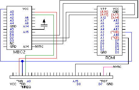
The Memory bank controllers (MBCs) ensured that the memory banks were shifted in the right place (the 8 bit CPU could only see 8 KB of ROM at a time) and also controlled the RAM in the cartridge. The MBCs had a register for this (5 bits on the MBC1, 4 bits on the MBC2) where the memory bank could be selected. MBC1 is controlled by A15..A13 and MBC2 by A15,A14,A8. The bank is in D0..D4 (D0..D3 for MBC2). When both RAM and ROM was present, A15 (low is ROM) controlled the selection.
The security protections of the Nintendo Gameboy
One of the most iconic handheld game consoles is the Nintendo Gameboy. When Nintendo released the Gameboy, they also thought carefully about copying protections of both the cartridges and the Gameboy hardware. For this they used some tricks that made it almost impossible for a long time to clone the Gameboy. Today there are a large number of emulators that mimic the behavior of the entire Gamboy in software. Most Gameboy clones (especially the Chinese clones) all contain a 16 or 32 bit processor that can run the complete Gameboy (and often other game consoles) perfectly. But when the Gameboy came on the market, this was not an option at all, so they chose to make it very difficult to “reverse engineer” the Gameboy. Nowadays the “reverse engineering” tools and methods have become so advanced that the Gameboy has also had to give up its secrets.
Nintendo was the first to make its own SOC (System On Chip) for the Nintendo Gameboy. This chip was made by the firm Sharp and was referred to by the name DMG CPU or Sharp LR35902. The processor part on this chip is a mix between the Z80 and the Intel 8080. It didn’t have the IY and IY (index) registers of the Z80, the register set is the same as the 8080. Also there are no IN and OUT instructions so there is no I/O space, all controls were memory mapped. In addition, have they added a few extra instructions that weren’t in the 8080 and Z80. There was also 8 KB of Ram on the chip. In addition, there was also a PPU for control of the on-chip LCD display and a simple four-channel Audio Processing Unit. Since this was all baked in one chip, without any kind of documentation (except probably for developers who signed a Non disclosure agreement), it was virtually impossible for a third party to Game Boy imitation. But that wasn’t all.
The CPU (or SOC) chip also contained 256 bytes of ROM code containing the bootstrap code. This code first performs a number of checks on the cartridge to see whether it is there correctly, but also meets a number of characteristics and a special checksum (control number) before the game will be started. One of the things to be checked was the Nintendo logo. This was also copied to the LCD and this was the familiar scrolling up logo on the screen at the Startup. When there was no cartridge in it, the code only read 0xFF (all bits on) which showed a black block on the LCD screen.
Then a checksum was made of the cartridge ROM and when it was not correct the Nintendo Gameboy froze and nothing was executed. Since this code was baked into the silicon, it could not be read in any way and was therefore a Nintendo secret. A few years ago fanatics have looked at silicon with a heavy microscope and discovered the code location and decoded the zeros and ones.
The 256 bytes ROM was able to disable itself, this was done by the last instruction in this ROM called “lock out”. This was also a security so that a cartridge could not read the internal ROM. Very cleverly done by Nintendo. A less smart move was that they only tested the first bytes of the Nintendo logo so there were jokers who changed the logo in a funny way.
Although there are currently many (Chinese) Gameboy / NES clones and a large number of emulators in software and even in FPGA chips, Nintendo certainly has successfully prevented copying/cloning of their products for the first few decades. They also have some of these protections in later products that are still applied. Various listings of the code of the Gameboy bootrom can be found on the Internet.
Specifications original Game boy
- CPU: 8 bit-Sharp LR35902 (Z80-compatible processor) 4.194304MHz
- RAM: 8kB internal
- VRAM: 8kB internal
- ROM: 256 kBit, 512 kBit, 1 MBit, 2 MBit and 4 MBit cartridges by mens of memory banking
- Display: LCD 160 x 144 dots, 4 shades of gray.
- Power: 6 Volts, 0.7 Watts – 4 AA Batteries
In my archive I found another PDF with the complete technical description of the Nintendo Game boy, everything about the special processor with missing and additional instruction set, the memory map, the sound and the video hardware, everything you ever wanted to know about the technique of the Nintendo Game Boy is in this deocument.
Intel MCS-51 processor family

Many years ago (1987) I was programming the 8052 professionally and I had all the assemblers and a PL/M compiler and an in circuit emulator at my development seat. At a certain point I knew the processor in and out and every trick it had. I really loved this processor, I started with an 8031 and external eprom but soon we switched to Atmel series of 8052 chips with internal flash memory. All of our low end modems had the 8052 as MCU in them. I even made a Basic version once but at the time modems needed much more processing power, we switched to Intel 80188 processors. But even nowadays I still used the STC and Atmel 8752 in a lot of electronic projects. I even build an 8052 programming IDE for Windows 10 / 11. I also collect old processors so I have a love of MCS-51 types of chips in my collection, not only from Intel but also from a lot of other manufacturers. On this page I give an overview of the MCS-51 family MCU’s and the different types.
I also have a Facebook Group on Retro Computing and Electronics, feel frtee to join!
About the MCS-51 processor family
The MCS-51 family succeeds the MCS-48 family, if you take a closer look at both you will see the resemblance. The architect of the Intel MCS-51 instruction set was John H. Wharton (21 Sept 1954 – 14 Nov 2018) who was an American engineer specializing in microprocessors and he did an amazing job. Intel’s original versions were very popular in the 1980s and early 1990s, and compatible derivatives remain popular up to today. It is an example of a CISC computer, but also has some of the features of RISC architectures, such as a large register set and separate memory spaces for program instructions and data. (Harvard architecture). Intel’s first MCS-51 family was developed using NMOS technology just like its predecessor Intel MCS-48, but later versions with the letter C in their name are in CMOS technology. This made them also more suitable for battery-powered devices. Nowadays Intel no longer manufactures the MCS-51 family processors but a lot of derivatives made by numerous vendors remain popular today and are still produced and even enhanced. The new MCS-51 based microcontrollers typically include extra features like an extra UART, extra timers, AD converters, Extra ports and internal eeprom memory to store the programming code. Also the original 8051 core ran at 12 clock cycles per machine cycle, with most instructions executing in one or two machine cycles. Enhanced 8051 cores are now commonly used which run at six, four, two, or even one clock per machine cycle and have clock frequencies of up to 100 MHz.
| Name | Int. ram | int. (ep)rom | I/O pins | Timers | Interrupts | Extra features |
|---|---|---|---|---|---|---|
| 8031 | 128 bytes | None(external) | 32 | 2 | 5 | None |
| 8032 | 256 bytes | None(external) | 32 | 2 | 6 | None |
| 8044 | 192 bytes | 4 Kb fact. mask rom | 32 | 2 | 5 | Slave processor build in SDLC protocol |
| 8344 | 192 bytes | None (external) | 32 | 2 | 5 | Slave processor build in SDLC protocol |
| 8744 | 192 bytes | 4 Kb UV eprom | 32 | 2 | 5 | Slave processor build in SDLC protocol |
| 8051 | 128 bytes | 4 Kb Rom | 32 | 2 | 5 | None |
| 8052 | 256 bytes | 8 Kb Rom | 32 | 3 | 6 | None |
| 8054 | 256 bytes | 16 Kb Rom | 32 | 3 | 6 | None |
| 8058 | 256 bytes | 32 Kb Rom | 32 | 3 | 6 | None |
| 8751 | 128 bytes | 4 Kb Uv eprom | 32 | 2 | 5 | None |
| 8752 | 256 bytes | 8 Kb UV eprom | 32 | 3 | 6 | None |
| DS89C420 | 256 bytes | 16 Kb Flash | 32 | 3 | 6 | None |
| DS89C440 | 256 bytes | 32 Kb Flash | 32 | 3 | 6 | None |
| DS89C450 | 256 bytes | 64 Kb Flash | 32 | 3 | 6 | None |
| DS80C320 | 256 bytes | None | 32 | 3 | 6 | None |
| DS87520 | 256 bytes | 16 Kb UV eprom | 32 | 3 | 6 | None |
| AT89C1051 | 64 bytes | 1 Kb Flash | 15 | 1 | 3 | Analog Comparator |
| AT89C2051 | 128 bytes | 2 Kb Flash | 15 | 1 | 3 | Analog Comparator |
| AT89C4051 | 128 bytes | 4 Kb Flash | 15 | 1 | 3 | Analog Comparator |
| AT89C2052 | 256 bytes | 2 Kb Flash | 15 | 1 | 3 | UART: Enhanced with Address Recognition SPI: Enhanced with Double Buffer |
| AT89C2052 | 256 bytes | 4 Kb Flash | 15 | 1 | 3 | UART: Enhanced with Address Recognition SPI: Enhanced with Double Buffer |
| AT89C51 | 128 bytes | 4 Kb Flash | 32 | 2 | 6 | ISP Flash Memory |
| AT89C52 | 256 bytes | 8 Kb Flash | 32 | 3 | 8 | ISP Flash Memory |
| AT89C55 | 256 bytes | 20 Kb Flash | 32 | 3 | 8 | Hardware Watchdog / Dual Data Pointer |
| AT89C51RB2 | 256 bytes | 16 Kb Flash | 32 | 3 | 8 | 1024 intre nal Xram / Hardware Watchdog / Dual Data Pointer / SPI Port |
| AT89C51RC2 | 256 bytes | 32 Kb Flash | 32 | 3 | 8 | 1024 intre nal Xram / Hardware Watchdog / Dual Data Pointer / SPI Port |
| AT89S51 | 128 bytes | 4 Kb Flash | 32 | 2 | 6 | ISP Flash Memory / Hardware Watchdog / Dual Data Pointer |
| AT89S52 | 256 bytes | 8 Kb Flash | 32 | 3 | 8 | ISP Flash Memory / Hardware Watchdog / Dual Data Pointer |
| AT89S8253 | 256 bytes | 12 Kb Flash | 32 | 3 | 9 | 3Kb Eeprom / SPI / ISP Flash Memory / Hardware Watchdog / Dual Data Pointer |
*) The AT89C52 / 51 and the STC89C52 / 51 are the most common used nowedays and common available.
The 8051 internals

*) It may look that the processor is very low on registers, but the whole 32 bytes of internal RAM is devided into 4 x 8 bytes register banks making a total of minimal 8 registers (with two of them being indirect address pointers) up to 32 internal registers in 8 bytes chunks.
8051 internal ram mapping
This ia the ram mapping, the first 32 bytes are reserved for register banks, but if you do not use these banks you can lso address then as common mamory. Then there us an eara that is bit addressable, again if you do not use this you can address these bytes as normal mamory bytes, you can even do both. The rest of the mamory up to 0x7f is common ram where also the stack lives. The area above 0x7f are Special Function Registers and when you write to them as
normal memory you will write directly into these registers. In the 8052 this upper 128 bytes of ram that is at the same address space as the SFR is only accessable with indexed addressing mode trough R0, R1 or DPTR. This can be tricky if you do not understand this completely. After reset the SP stack pointer is at address 0x07, one of the first things I dos is set this to a safe address.
SFR registers on different types of 8051
| 0 / 8 | 1 / 9 | 2 / A | 3 / B | 4 / C | 5 / D | 6 / E | 7 / F | |
|---|---|---|---|---|---|---|---|---|
| F8 | ||||||||
| F0 | B | |||||||
| E8 | P4 | |||||||
| E0 | ACC | WDT_OONR | ISP_DATA | ISP_ADDRH | ISP_ADDRL | ISP_CMD | ISP_TRIG | ISP_CONTR |
| D8 | ||||||||
| D0 | PSW | |||||||
| C8 | T2CON | T2MOD | RCAP2L | RCAP2H | TL2 | TH2 | ||
| C0 | XICON | |||||||
| B8 | IP | SADEN | IPH | |||||
| B0 | P3 | |||||||
| A8 | IE | SADDR | ||||||
| A0 | P2 | AUXRT | ||||||
| 98 | SCON | SBUF | ||||||
| 90 | P1 | |||||||
| 88 | TCON | TMOD | TL0 | TL1 | TH0 | TH1 | AUXR | |
| 80 | P0 | SP | DPL | DPH | PCON |
- Standard 8031 / 8051 SFR registers.
- Extra 8032 / 8052 processor.
- Extra 8952 processor.
The AT89C52 datasheet has a discription of all SFR registers.
PINOUT of the 8051

Pin 1 to Pin 8 (Port 1) Pin 1 to Pin 8 are assigned to Port 1 for I/O operations, they can be configured as input or output pins, if logic zero (0) is applied to the I/O port it will act as an output pin and if logic one (1) is applied the pin will act as an input pin.
Pin 9 (RST) The reset pin is an active-high input pin. If the RST pin is high for a minimum of 2 machine cycles, the microcontroller will reset, it is often referred as power-on-reset. In normal circuits this is done with simple capacitor and resistor and if you want a reset button, you can add this parallel to the capacitor.
Pin 10 to Pin 17 (Port 3) These pins are I/O port 3 pins, these pins are similar to port 1 and can be used as universal input or output pins. These pins also have some additional functions which are as follows:
- (10) P3.0 (RXD) : Serial data receive pin which is for serial input.
- (11) P3.1 (TXD) : Serial data transmit pin which is serial output pin.
- (12) P3.2 (INT0) : External Hardware Interrupt 0.
- (12) P3.3 (INT1) : External Hardware Interrupt 1.
- (13) P3.4 (T0) : Timer 0 external input, tis pin can be logical connected with a 16 bit timer/counter.
- (14) P3.5 (T1) : Timer 1 external input, tis pin can be logical connected with a 16 bit timer/counter.
- (16) P3.6 (WR’) : External memory write, you have to use this pin when you add external SRAM.
- (17) P3.7 (RD’) : External memory read , you have to use this pin when you add external SRAM or ROM.
Pin 18 and Pin 19 (XTAL2 And XTAL1) These pins are connected to an external oscillator which is generally a quartz crystal oscillator with two small capacitors.
Pin 20 (GND) This pin is connected to the ground (0V power supply).
Pin 21 to Pin 28 (Port 2) Pin 21 to pin 28 are port 2 pins, these pins can be used as general I/O pins. But when you use external memory these pins provide the higher-order address byte A8..A15.
Pin 29 (PSEN) PSEN stands for Program Store Enable. It is and active-low output pin to read external code memory, this pin is connected to the OE pin of the ROM.
Pin 30 (ALE) ALE stands for Address Latch Enable, it is an active-high output pin, this pin is used to latch the low address (A0..A7) of port 0 to an external latch and when not active port 0 is the data in and output.
Pin 31 (EA) EA stands for External Access input. It is used to enable / disable external memory interfacing. If EA is connected to Vcc the chip will use the internal ROM, when this line is connected to GND the chip will use the external ROM.
Pin 32 to Pin 39 (Port 0) Pin 32 to pin 39 are port 0 pins that can be used as normal bidirectional I/O pins, however they don’t have any internal pull-ups. These pins also used as bidirectional Data bus and provide the low part of the external; address (D0..D7) when ALE is active. When used as data / address lines they can no longer be used as I/O pins.
Pin 40 (VCC) This pin provides power supply voltage to the chip, most of the time 5 volt, but some variants use 3.3 volt.
Minimal hardware design schematics

This is the typical design you will find on the (Chinese) minimal hardware boards (they often add a power supply as well) and it uses the internal ROM / EPROM code and the internal ram only. I have written lots of hardware using this design, the internal ram is verry useful because of the bit addressable area that can be used as Booleans (flags) in a program, and with the 4 register banks it is easy to write simple interrupt handlers, just switch the bank on an interrupt and switch it back before you leave the interrupt routine. When using an 8752 you have the extra high 128 bytes of internal ram and the code can be easily burned over and over again in the Flash eprom on chip. This configuration has a LOT of available I/O lines, a serial input output, timers and interrupt so its is very nice to use in embedded systems. For instance you could build a complete full keyboard interface, just using this simple design. For programming the chip you can use an eprom programmer or you can use In Circuit Programming with and USB adapter on several family members of Atmel and STC.
Minimal basic computer hardware design schematics

This design uses internal code and externa 64 Kb SRAM, you can see that port 0 and 2 are external data and address lines and we use the RD and WR pin of port 3. In this design I used an original 8052-basic chip from Intel, but you can also use an AT89C52 from Atmel or STC to program the basic code into the Flash rom of the 8052 processor. This design uses a 8052 because it needs the 256 bytes internal ram. You can find the sourcecode of the basic versions 1.0 and 1.3 in the example directory of my 8052 IDE program (also on this site). You have to connect this design with a USB TTL / serial adapter to a PC or to a TTL compatible terminal. It will do autobaud on pressing the spacebar. Just build this
design, upload the code into a 8052 and you have a working floating point Basic interpreter based microcomputer that can also use the unused pins to control external hardware.
Full external eprom and ram design schematics

This is the most complex design I made with a 64 kb external ROM / Eprom / Flash rom and 32 Kb of ram. I use 32kb of ram because these chips are commonly available and otherwise you would have to switch the next step and that is a 128 kb ram of which you only use half. In my case 32 Kb is more than enough for all cases. If we look at the design we see the same address latch and for the ram a little more logic to generate the output enable signal. This is a safe design. I also added a reset button and a EA selection pin if you want to use the board also to run code inside the 8051 chip. The design is not that complex, the 51 family is a very easy to implement microcontroller. Also in this design you
have a lot of free I/O ports to control anything. It also uses a TTL level serial interface.
Adding a real RSR232 interface

If you want to connect a 8051 to a read RS232 terminal you will need a RS232 level converter chip. If you do not know what RS232 is look here. This is my simple basic design for a RS232 interface, you can use this on almost every single board computer design, it does not support any control lines, just the basic TX and RX lines. It uses the MAX232 chip
that is still commonly available. Personally I like to keep things simple.
It is fun writing code for the 8051 family processors, they are very fast, have a lot of I/O ports, a very nice instruction set and when you take the challenge of building a complete application just using 192 bytes of ram you will find that especially the bit addressable area is very clever to store flags, a Boolean value will only take up one BIT of memory. I have written a very complete developers IDE for the 8051 processor that also supports the 89c52 hardware. It has a assembler, disassembler, emulator, single step debugger, TV100 terminal, seven segment displays and output leds on board. Also I provide som example code and some sourecode from Intel. For a good understanding of all the instructions and tips and tricks, there are nice books and online tutorials, this page is intended as a guide to the internals and te hardware design of this wonderful chip.
Mini Arduino Nano gamecomputer
Sometimes certain parts invite you to make a nice application and in this case it was a few analog joysticks in combination with an Arduino Nano and a small OLED screen. All the ingredients to make a small game console. Since the display only needs two connecting wires (I2C) and the analog joysticks need two analog inputs each an Arduino Nano had more than enough pins. The whole can then be powered with four AAA batteries. I have the Arduino Nano and the display in header pins so that they can possibly be replaced or reused themn. This also better than solder directly onthe pins of these components. The Arduino Nano I have is situated in the middle of a bit of experimentation
board with both joysticks on either side. To save space I placed the display above the Arduino Nano and then I connected everything to the Arduino and added the power supply line with short wires. For the batteries I bought a ready-made holder with switch, this is handy because then we don’t need to place an on and off switch somewhere. This was the whole (simple) hardware design, now it was important to write some software. I had already written a library for the display, so it could be nicely reused and the choice fell on three games that I had already made in the past, snake, pong and breakout. I wrote these games so that they can be played with either one or two people, who can sit opposite each other. Then I wrote an easy choice menu and the game console was ready. The source code of both the library and the games is at the bottom of this page as download. The design and software are not copyrighted (it’s GPL) and I hope I can help people with this inspire them to make their own version and, for example, design a nice housing, write new games or improve or supplement the old games. I wish everyone good luck and a lot of fun with this design and at my home the kids had a lot of fun with it.

Arduino Nano
The Arduino Nano is also a very small Arduino board that is especially suitable for use on a breadboard because the connector pins can be put on the bottom side. This makes it easy to plug the board into a breadboard. The board is based on the well-known ATmega328 (Version 3.x) or ATmega168 (Version 2.x). There is no power plug on the board, but there are power input pins. The board can be powered through the Mini-B USB connection, 6 to 12V voltage on the raw input or 5V stabilized power on pin 27. The voltage source will be automatically selected from the best of the three. The Arduino Nano can be programmed via the built-in USB port. The board can be programmed with the standard Arduino programming IDE, you can board and simply select the port from the drop-down menu. The possibilities of the small board are very wide but the design is specially made for use on an experiment board (breadboard).
- Chip: ATmega328 / ATmega168 16 Mhz
- Voltage: 5 V
- Voltage raw: 7 – 12 Volt
- Digitale pins: 14 ( 6 PWM)
- Analoge inputs: 8
- Size: 45 mm x 18 mm
- SRAM: 1 KB (ATmega168) or 2 KB (ATmega328)
- EEPROM: 512 bytes (ATmega168) or 1 KB (ATmega328)
- Flash: 16 KB (ATmega168) or 32 KB (ATmega328)

Oled Display Module for Arduino 0.96 128×64 I2C
The display I used is a fairly standard OLED cheap display with white pixels, a resolution of 128 x 64 pixels and a control by means of I2C by the the SSD1306 driver IC. This shield also only needs two data lines and it consumes minimal current so that it can also be used in projects that need to be powered by a battery or battery. The size of this screen is slightly larger than the previous one and measures 26.0 x 15.0 mm. The module runs on 3v3 and can be connected to the outputs of the 3v3 output of the Arduino, where the I2C lines can simply be connected to the 5V Arduino pins. The I2C address of this OLED shield is 0x3C by default. The screen is very clearly readable due to a very high contrast. Because it uses 128 x 64 pixels you do not lose more than 1 Kb of valuable sram for this display with the Arduino. The SSD1306 is a single-chip CMOS OLED/PLED driver with controller for displays with a maximom resolution of 128 x 64. The IC contains a display controller with display RAM and a built-in oscillator so that it can be used with minimal external components. It has a built-in 256 steps brightness control. It has a 6800/8000 series compatible Parallel Interface and a I2C interface.
Pins of the 128×64 display
- 1 Vcc: -> 3v3
- 2 Gnd -> Gnd
- 3 Scl -> A5 (SCL)
- 4 Sda -> A4 (SDA)
Link: Datasheet of the SSD1306 controller.

Analoge joysticks voor de Arduino.
An analog joystick is like two potentiometers connected together, one for vertical movement (Y-axis) and another for the horizontal movement (X-axis). So these yield an analog resistance value that can be easily converted into a voltage readable by the analog input pins of the Arduino, The position of the joystick then corresponds to the voltage and will be between 0 and 1023, with 512 being the center point. In addition, there is a pressure switch underneath that can be connected to a a digital pin of the Arduino. In this design I eventually use the analog inputs as digital by converting the voltage into three values, center, left and right, as this is more convenient for programming. The connections of the two joysticks are on the following pins of the Arduino Nano:
#define BUTTON_PIN1  7
#define BUTTON_PIN2  6

#define XPIN1       A7
#define YPIN1       A6
#define XPIN2       A2
#define YPIN2       A1
Link: Website with example about the analog joysticks.
Arduino Nano game console links, files downloads
Arduino ATtiny ISP programming board

After making several projects with various Arduino boards, I started to use smaller and smaller boards and I ended up with a standalone processor chip. And for some applications, the standard 28-pin chip is still a bit too large. My eye had already fallen on the ATTiny85, but the 8 connection pins scared me off. But after I give the chip a good look and when I had a closer look at it, I noticed its strength. The small chip contains a full Atmega processor with flash programming memory and RAM on board with also a built-in crystal oscillator. So it is a real single chip computer
with 6 (5 effective when you want to keep the reset pin for reprogramming) in or outputs that also have additional functions such as Interrupts, PWM and analog. Each pin is freely programmable for a function and whether you want one input and five outputs or vice versa, it’s all possible with this little chip. But the chip can also communicate using I2Ch, for example to connect a screen or multiple sensors or control lights or motors with the designated PWM output pins. When I started thinking about this, I suddenly saw a lot of possibilities, the chip costs between 1 and 3 euros and can replace a complex electrical circuit. There are also a number of links on this page to sites that have done impressive things with this tiny ATTiny chip. Small boards are available with a USB port with an ATTiny85 on it, but the chip can of course also be used as a standalone chip. To program the ATTiny you will need an ISP programming board, but this is a task that our older trusted Arduno Uno can do for us. On this page there is also a small set-up board for the Arduino Uno with which the ATTiny chips can be programmed from the standard Arduino development environment.
Atmel also markets several models with the ATTiny in different housings. I’m only going to cover the the 8 pins versions here. With larger versions I quickly tend to take the 28 pins Atmega328 again because this chips is almost the same price or sometimes even cheaper. As we are used to from Atmel, there are several versions with different amounts of Flash rom and sram memory with different prices as well. By default they have a built-in RC oscillator that is not super accurate but keeps two pins free, an external crystal can also be used by sacrificing two pins oscillator to be attached. The ATtiny85 works by default on a 1 Mhz built-in RC oscillator but this can be increased by loading of the software.
| Device | Flash (Mb) | RAM byte | EEPROM byte |
|---|---|---|---|
| ATtiny13 | 1 | 64 | 64 |
| ATtiny25 | 2 | 128 | 128 |
| ATtiny45 | 4 | 256 | 256 |
| ATtiny85 | 8 | 512 | 512 |

Download the ATTiny13 datasheet.
Download the ATTiny25 /45 / 85 datasheet.
Arduino ATTiny programming
To program an Arduino you need software, the Arduino programming environment. This free development environment can be found at: download Arduino IDE here . This environment is suitable for Windows, Linux and Mac OS X. When you have connected the computer to the Arduino board wtth a USB cable, you can transfer the program code directly to the Arduino board. You can write the program on your own computer and “upload” the code to the Arduino board. All you need to do is select the board type in the menu and the port you are using on which the board is connected (when there are multiple ports). There is really only one programming language popular for the Arduino and that is the programming language C and C++. The programming environment includes a large amount of standard libraries for LCD, Servo, motors, wifi, etc. and all of these are free to download. The Arduino C version deviates from the C standard on a few points and unfortunately not all functions are present in the supplied libraries. Of course it is still an 8 bit processor and for example the support of double variables is a bit flawed. Where a standard C program starts with a main() routine, an arduino program (often called a sketch) consists of two program blocks, the setup() and the loop(). At the beginning of the program is the “void setup()” and in this function allows initialization of the program such as initialization of I/O pins, initialization of software libraries, and global variables. The setup() function is executed once by the arduino at program startup. Then it is the turn of the loop() function, it will be called endlessly until the power is turned off. From this loop() function you can call other functions and so you can build a structured program.

Arduino ATTiny default pin modes
A common source of confusion appears to be the function and numbering of the in/out pins of the aTtiny processor. I searched myself on the Internet and read the datasheets and came to the following simple overview that makes everything clear. Each pin has a different internal number and function depending on how it is configured with pinMode() and whether one uses analogRead, analogWrite, digitalRead or using digitalWrite. To make it clear I have put this in an excel sheet of which a printout is here. You don’t have to go through the internet registers to program the function of the pins, unless you want to use the alternative functions of the pins. The standard IDE and the chip definition herein will do most of the work for you when you specify the pins in the standard way.

To be able to program the ATTiny, you need an ISP programming board and these are also available in various versions. These programmers are not cheap and if we already have an Arduino Uno, we can easily use it as an ISP programmer as an extra task. You can build a small circuit on a breadboard every time you want to program an ATTiny, but when you you want to program more often, a small shield for the Arduino Uno is more convenient. We build this on a small piece of experiment print and you will need a pair of header pins, an 8 pin IC socket, a LED, one 220 ohm resistor and a 10 uF capacitor. And of course a soldering iron, solder and mounting wire, preferably in different colours.
I chose to put the solder side up, this makes soldering the headers much easier and the rest of the components can just as well be soldered on the top side. The connection wires are then hidden at the bottom.

I sawed off a piece of experimental PCB of 10 holes wide and 20 holes long. On one side is the (8) row of pins are on the far left and the other side all the way to the right. I plugged the pin rows into the Arduino first. On the power supply side and the reset pin I use the entire set of last pins, the unused pins serve as reinforcement. To polarize the board to prevent it from putting it in the wrong way I added two femnale header pins next to the male ones. On the other side the row of pins ends at the middle separation, leaving two pins free at the usb connector. Then I push the PCB over the pins and I carefully solder the pins. Don’t use too much solder, we don’t want pins to connect. Then we also bend the pins of the IC socket to the side and solder it somewhere in the middle of the PCB. I put the 1 pin on the side of the USB and power plug myself and marked it extra with a thick tip of a black marker. Then the PCB can be removed from the
Arduino Uno. At the top of the PCB (the solder side) we now put the LED and the resistor between the negative supply voltage pin and pin 5 of the ATTiny socket. Please pay attention to the polarity of the LED, you can test whether it is seated correctly by putting the plus on the pin of the foot and the minus on the header pin. Now we can do it turn the PCB over for the rest of the wiring.

We now connect pins of the power supply to the IC socket, the plus 5 volts goes to pin 8 and the Gnd to pin 4 of the socket. Now we can solder the small capacitor of 10 uF between the Gnd and the Reset pin of the Arduino Uno pay attention to the plus and the minus of the capacitor (minus to Gnd) and place the capacitor a little parallel to the header pins so that it will be sits neatly next to the Arduino chip. Now we solder the remaining wires between the Arduino Uno pins and the IC socket. Which Arduino pin to which pin of the foot is shown in the diagram below. Pay particular attention to using little solder so that there is no short circuit and if necessary, use the tip of a small screwdriver between the solder spots to remove small tin residues. Then we are going to test whether everything works by inserting an ATTiny into the socket and plugging the shield onto the Arduino Uno. Now connect Uno to the
computer with a USB cable, the Arduino Uno should work normally and the shield will do nothing. To switch the Arduino Uno to ISP programmer, let’s take the shield off again.

Adjust the Arduino IDE
To be able to program the ATtiny85 we first have to upload the ISP sketch in the Arduino Uno. You can find this sketch in example files included with the Arduino IDE which can be found in file -> Examples and the sketch is called ArduinoISP. Connect the Arduino Uno without shield to the computer and upload this sketch to the Arduino Uno in the usual way. Now let’s get the Arduino the IDE to support the Attiny. In the screen that you can find under File -> Preferences, search for the input field “Additional Board Management URL” and enter the following URL:
Then press the OK button to save the setting and close the screen. Then go to Tools -> Board -> Board Manager and search all the way down to the block that says “attiny by Davis A. Mellis” and click install. After installing, you should see a new board in the selection screen for the boards. Here you select the board, the processor and the choice for Arduino as ISP and then you put the shield on the Arduino. Now you can load the Blink sketch where you have to change the LED pin to 0 because we have the LED on this pin. When you connect the Arduino with the shield to the computer you should be able to upload this sketch using the normal upload button to the ATtiny, after which it will flash happily. This didn’t work for me at all and the IDE gave an error about a device number 00000, after checking it turned out that a solder connection on the IC socket was not good. After this it works fine and I could use my ATtiny85
with the blink sketch.
ATtiny with external crystal
I made a small extension to my programmer board. In one of my first experiments I made a mistake and I accidentally installed a bootloader with an external crystal after which the attiny85 chip stopped responding. So I couldn’t use the bootloader to make the ATtiny85 work on the internal oscillator again. The bootloader sets the “fuses” that determine whether the chip uses an internal or external clock. If the chip is set to external and there is no crystal, the chip will not boot. The only way to reprogram the chip is to connect an external crystal. So I decided to install an external crystal of 8 Mhz on the PCB in a small socket so that I could remove it again for checking. The crystal has a a 22 pF capacitor to ground on both legs. The capacitors can remain in place when the crystal has been removed. After placing the ATtiny85 on the board with the crystal, I selected the 1 Mh internal boatloader that I could then upload successfully after which the Attiny also worked without the crystal. By means of this extension I can now also load code that will use eventualy use an external crystal in the final circuit of the Attiny processor.
Nice ATtiny applications
Link: Tiny robot family Gallery
Link: Terminator 2 – Micro robot
Link: ATTiny Line Follower
Link: ATtiny-Powered Arduino Projects
Link: attiny – The Garage Lab
Link: ATiny mini spelcomputers
DIY PIC development board

I bought a PICKIT3 In Circuit Programmer unit and a dev board, but that was only for 40 pins PIC chips and I also want to use 28 pins PIC chips, for smaller designs that do not need so many pins. I looked in several shops but could not find anything that would fit my needs, so I decided to design and build one myself. It is not that hard, there are lot of example designs and after looking at them I had a good idea of what I wanted. So after one night designing and two nights soldering, I was finally able to test my design. I works like a charm.

It has a 40 pins ZIF socket and a 28 pins ZIF and all programming lines, onboard LED and switch are shared by both sockets, and a reset button that is shared by both sockets, but every socket has its own crystal oscillator circuit. It has a USB power supply, but during programming the power comes from the PICKIT3 device. It has a power indicator led, and two header rows of ground and plus 5 volt, to power devices you want to connect. I put header pins beside both sockets (both sides) so that every pin of the PIC processor is available to devices you want to connect. The onboard led is on pin RA0 and the switch is on port RE2 with a pullup. Both led and switch are connected to the PIC with a jumper so they can be disconnected if they are in the way.
There is one big restriction, you can only have ONE chip on the board, never two at the same time because the pins are hardwired together.
The board also has both the TX and RX lines (and Ground) on a header so you can connect it to a serial port using an TTL to RS232 cable. The crystals of the oscillator circuit are placed in a header pin socket so they can be replaced easily, I use 4 Mhz crystals (just like the original dev board), but you can choose anything that fits your needs and matches with the PIC processors.
I use MPLAB as a development suite and I can connect MPLAB with the PICKIT3 adapter to this board, edit my ‘C’ source code and upload it to the PIC processor on my dev board with just one click. This makes PIC processor development nice and easy.
LCD display on 8952 dev board

I have a cheap 8952 dev board from China and I added a Arduino Nano as ISP programmer to it so I can upload the code easily. This works fine but the dev board is a little limited in I/O, it only has a few buttons and eight led. There is a connector for a 1602 LCD display, but no supporting code. So I took up the challenge of making this myself. On this page you can find the 8051 assembly code of a simple LCD driver using the HD44780 type of driver. I have written code for this driver in the past so it wasn’t a complete surprise. The connections are quite obvious, I put them as equates in the beginning of the code so you can easily switch them to other pins on your design.
; ---------------------------------------
; 8052 LCD interface
; Hein Pragt 2023
; ---------------------------------------

// commands
LCD_CLEARDISPLAY	equ	01H
LCD_RETURNHOME		equ	02H
LCD_ENTRYMODESET	equ	04H
LCD_DISPLAYCONTROL	equ	08H
LCD_CURSORSHIFT		equ	10H
LCD_FUNCTIONSET		equ	20H
LCD_SETCGRAMADDR	equ	40H
LCD_SETDDRAMADDR	equ	80H

// flags for display entry mode
LCD_ENTRYRIGHT		equ	00H
LCD_ENTRYLEFT		equ	02H
LCD_ENTRYSHIFTINCREMENT	equ	01H
LCD_ENTRYSHIFTDECREMENT	equ	00H

// flags for display on/off control
LCD_DISPLAYON	equ	04H
LCD_DISPLAYOFF	equ	00H
LCD_CURSORON	equ	02H
LCD_CURSOROFF	equ	00H
LCD_BLINKON	equ	01H
LCD_BLINKOFF	equ	00H

// flags for display/cursor shift
LCD_DISPLAYMOVE	equ	08H
LCD_CURSORMOVE	equ	00H
LCD_MOVERIGHT	equ	04H
LCD_MOVELEFT	equ	00H

// flags for function set
LCD_8BITMODE	equ	10H
LCD_4BITMODE	equ	00H
LCD_2LINE	equ	08H
LCD_1LINE	equ	00H
LCD_5x10DOTS	equ	04H
LCD_5x8DOTS	equ	00H


EN_PIN 		equ	p1.0
RW_PIN 		equ	P1.1
RS_PIN 		equ	P1.2
LCD_DATA	equ	P2


	CSEG

	ORG	0000H

	call	lcd_init
	call	lcd_home
;
	mov	a,#0
	mov	b,#3
	call	lcd_pos
;
	mov	dptr,#hello
	call	lcd_print

	mov	a,#1
	mov	b,#3
	call	lcd_pos

	mov	dptr,#hein
	call	lcd_print
loop:
	jmp	loop


hello:
	db      'Hello World',0
hein:
	db	'Hein Pragt',0

; -------------------
; Init LCD display in 8 bit mode
; -------------------

lcd_init:
	clr	EN_PIN
	clr	RW_PIN
	clr	RS_PIN
	mov	a,#0
	mov	LCD_DATA,a	; Data, RS and R/W low
	mov	r6,#15
	call	delay		; Delay 15 Ms
;
	mov	a,#(LCD_FUNCTIONSET + LCD_8BITMODE + LCD_2LINE)
	call	lcd_command
	mov	r6,#5
	call	delay		; Delay 5 Ms
;
	mov	a,#(LCD_FUNCTIONSET + LCD_8BITMODE + LCD_2LINE)
	call	lcd_command
	call	delay1ms	; Delay 1 ms
;
	mov	a,#(LCD_FUNCTIONSET + LCD_8BITMODE  + LCD_2LINE)
	call	lcd_command
	call	delay1ms	; Delay 1 ms

	mov	a,#(LCD_FUNCTIONSET + LCD_8BITMODE + LCD_2LINE)
	call	lcd_command
;
	mov	a,#(LCD_DISPLAYCONTROL + LCD_DISPLAYON + LCD_CURSOROFF + LCD_BLINKOFF);
	call	lcd_command

	mov	a,#(LCD_ENTRYMODESET + LCD_ENTRYLEFT + LCD_ENTRYSHIFTDECREMENT)
	call	lcd_command
	call	lcd_clear
	ret


; -------------------
; Send CLS command to LCD
; -------------------

lcd_clear:
	mov	a,#LCD_CLEARDISPLAY
	call	lcd_command;
	mov	r6,#50
	call	delay		; Delay 50 ms
	ret

; -------------------
; Send Home command to LCD
; -------------------

lcd_home:
	mov	a,#LCD_RETURNHOME
	call	lcd_command;
	mov	r6,#50
	call	delay		; Delay 50 ms
	ret

; -------------------
; Send cursor
; a = row 0,1  b = col 0.16
; -------------------

lcd_pos:
	anl	a,#01H
	jz	row0
	mov	a,#40H	; row1
row0:
	orl	a,#LCD_SETDDRAMADDR
	anl	b,#0fH
	orl 	a,b
	call	lcd_command;
	mov	r6,#50
	call	delay		; Delay 50 ms
	ret


; -------------------
; Print 0 tyerm string in DPTR
; -------------------

lcd_print:
	clr	a
	movc	a,@a+dptr	; Read char
	inc	dptr 		; Bump pointer.
	jz	prt_end
;
	call	lcd_char	; print char
	ajmp	lcd_print	; Loop
prt_end:
	ret


; -------------------
; Send char to LCD
; char is in A
; -------------------

lcd_char:
	clr	RW_PIN
	setb	RS_PIN
	clr	EN_PIN
	setb	EN_PIN
	mov	LCD_DATA,a
	clr	EN_PIN
	setb	RW_PIN
	clr	RS_PIN
	acall	delay1ms
	ret

; -------------------
; Send command to LCD
; command is in A
; -------------------

lcd_command:
	clr	RW_PIN
	clr	RS_PIN
	clr	EN_PIN
	setb	EN_PIN
	mov	LCD_DATA,a
	clr	EN_PIN
	setb	RW_PIN
	acall	delay1ms
	ret


; =======================================
; General subroutines
; =======================================

; -------------------
; Delay R6 x 1 Ms
; -------------------

delay:
	call	delay1ms
	djnz	R6,delay
	ret

; -------------------
; Delay 1 ms
; -------------------

delay1ms:
	mov	TMOD,#01H	; Mode 1
	mov 	TH0,#0FCH
	mov	TL0,#018H
	clr	TF0
	setb	TR0
dellp1:
	jnb	TF0,dellp1
;
	clr	TR0
	clr	TF0
	ret


	END
Yo can download the code here: Download lcd_display.zip

I hope this is useful and inspires you to add new features, or use it in one of your own project, for me it was fun to write 8051 assembly code again.
27xx eprom replacement

One of the big problems of retro computing is that some parts are no longer available. Old designs sometimes use the 2708 (1K eprom) or the 2716 (2K eprom) and these are hard to get and require a old (25 Volt) eprom programmer to program. Sometimes it is just better to replace them with a later version. But the later eproms like the 2764, 27128 and 27256 are not pin compatible. Even replacing the 2708 with a 2716 can cause a big problem and defective chips. I got a question of someone who wanted to replace the 2708 of a Elektuur Junior computer board, with a 2716 eprom. I have some 2716 eproms but my eprom programmer does not go higher than 18 volt, so I could not program it. What I also had were a few 2816 5 Volt eeprom chips, these are 2716 compatible eeproms. I decided to program one of these, but with a notice that the pins should be redirected.
The eprom of the Junior computer

As you can see this old eprom uses +5, -5 and 12 volt to operate, supplying these voltages to a “modern” chip would certainly destroy them. So we need a conversation board, or we could bend out some pins and connect them with the right voltage levels using small wires.
Different pins on 2708, 2716 and 2816

As you can see there are four pins (18-21) that are different and require other levels.
The correct levels for all eproms

The main difference between the 2716 and the 2816 (according to the datasheet) is that the 2716 needs to have pin 18 to Vcc and the2816 to the Gnd. The eprom will use (select) the lowest “bank”so 0000H. The best solution for the Elektuur Junior computer seems to be a small conversion board or bend out pins 18, 19 and 21, to wire them to the correct voltage levels. With a conversion board you can easely switch the (e)eprom, with bend out pins you will need to solder to replace the (e)eprom. I have seen small adapter PCB’s on the market for those who cannot or won’t solder.
MK14 emulator (Windows)

This page is about my MK14 emulator for Microsoft Windows. The the INS8060, also called the SC/MP processor was the first real processor I studied when I was 13 years old, but at that time I did not have much money,so I could not afford to buy a real computer board. I read all I could about the SC/MP processor and I would draw the internal of the processor on a big piece of paper, with the RAM / ROM / keyboard and display as registers and I would have a lot of small zero and one papers to simulate the flow of the bits and bytes in the (paper) circuit. Looking back this was ridiculous, but this is the way I learned computer design and binary logic. The SC/MP is my first processor and nowadays you cannot get the processor anymore (at least not at a reasonable price), but there are emulators in software and hardware that are still available. After building two PIC14 boards I decided to also write an emulator of the MK14 for Microsoft Windows. I dedicate this program to Karen Orton (R.I.P.) who left us the amazing PIC14 hardware emulator.
I respect copyright and I will not distribute illegal software. But this program includes the MK14 rom, and the zip file includes some old programs and documents that still might be copyrighted. BUT in my opinion the copyright was from 40 to 45 years ago, these products have not been on the market for a lot of years and I think that no one would not care if someone was using a 40 year old file on their own Windows 10 machines. I do not ask any money for this package and the main goal is to keep the old spirit alive. I anyone can identify him or herself as a legal copyright owner and has problems with the distribution I will remove that content. But I seriously believe there is no one to object to distributing these old artifacts as freeware. My program itself is closed source but freeware.

This emulator of the MK14 has full memory expansion on 200H, 800H and B00H and the first 0x200 bytes contain the second version of the MK14 rom. The on screen keys work as they should do, you can also us the keys on your keyboard, the mapping of the command keys is on top of the key. You can load programs in hex format using the top menu, the last digits of the filename is the starting address. Press reset or abort then enter the address and push the go button. You can also save the memory to a hex file, the first option only saves the original memory 0xf00 to 0xfff, the second option saves the entire ram from 0200 to 0fff. The instructions are cycle precise and the emulator runs on the same speed as an original MK14 would, so it can be slow sometimes, but its real.

This is a so called portable program, you do not need to install it. Just download the zip file and unpack it on an logical location on your disk. I have all my portable application in a top directory “portapps”. There is a win62 and a win32 version of the emulator, both are digitally signed for your safety. There is also a directory containing a lot of example programs I collected, with sourcecode and hex files. The is also a documentation directory that contains the original MK14 manual and some SC/MP programming manuals and datasheet.
Download
You can download the zip file here: mk14_emu101.zip
Version 1.01
- First (beta release) version, the program has been testen by myself on my hardware.
Have fun, regards, Hein Pragt.
USB keyboard on an Arduino

The Arduino does not have a standard USB interface to connect a USB keyboard. Many microcontrollers do not have a USB Host controller as standard interface. It is possible to buy a USB host shield and connect it to the Arduino or microcontroller, but these are often expensive shields and the interface is also often difficult to program. The PS/2 protocol for keyboards is quite simple, it consists of a serial clock and data line and every character that will be struck will be sent out serially. Something that almost every Arduino or microcontroller standard can do .
Now, there are those little USB to PS/2 adapters out there, and to be honest there’s NOTHING in them except a few jumper wires. Manufacturers didn’t feel like making a separate USB or PS/2 keyboard, so they came up with a keyboard controller that could do both. At startup the controller looked at the data – and data + lines and when both were positive with a 10K pullup, the keyboard went into PS/2 mode. If not, it went into USB mode. It is therefore very easy to connect a standard USB keyboard via a standard USB plug and use two resistors to indicate that the keyboard must communicate with PS/2.
Then how do we connect this to an Arduino or microcontroller. First, we have a data line that carries the serial data and a clock line that provides the clock for the data line. It is therefore a good idea to connect the clock line to an interrupt pin and read the data line at each interrupt and shift it into a register. With an Arduino Uno it looks like this:

For the Arduino there is a standard library for reading and decoding a PS/2 keyboard, this is written in C and can be “translated” to a microcontroller. So you don’t have to do anything for the Arduino and it’s nice that the standard serial line remains available. The Arduino library can be found here: http://www.pjrc.com/teensy/arduino_libraries/PS2Keyboard.zip
I have seen several variants of the PS/2 library, it is worth looking further to see if it is also available for the hardware you want to use. BUT… connecting and converting a USB to PS/2 keyboard is a piece of cake. Have fun building your own, Hein Pragt.
8031 Arduino Mega (Eng)
This is a fun project based on an Intel P8031 processor (may be any higher version such as 8051, 8052, etc.) a small 8031 shield and an Arduino Mega board. This allows you to experiment with a real 8031 processor where the ROM, external RAM and serial I/OI are all provided by the Arduino Mega. In effect, this gives you an 8031 based computer, with up to 64KB of ROM, 6KB of external RAM and serial I/O. In addition, you have all pins of P1 open to connect external hardware to it and all other connections of the 8031 processor are also routed out. I myself threw the software that originally came with the 8031 retroshield into the trash and wrote new Arduino software. This has been improved on many points and no longer needs external libraries.
In addition, a Paul Monitor was included as standard, but you can’t do much with it. It’s nice that it works but it’s not a nice demo. I decided to dust up an old version of Tiny Basic that I had once modified. This was a bigger job than I imagined, I also wanted the code to run on a bare 8031 with 128 bytes of ram and for that everything had to be rewritten to the external ram. I also did a major code cleanup and organized and formatted the code neatly and clearly. On this page I provide a zip file with the source code of the basic interpreter in 8031 assembly.
Hardware
The hardware you need is an 8031 retroshield, which you can order HERE. You also need an 8031 processor, which I sell in my webshop, and you need an Arduino Mega board. One of the minor tweaks I made to the hardware is on the 8031 retroshield. According to the datasheet, the X1 pin must be grounded when the 8031 is controlled with an external clock. The photo shows how I did this on the back of the PCB with a solder bridge.

So I did this and so I only had to solder the resistor for the X2 line. The rest of the capacitors, the resistor and the LED are actually superfluous and I didn’t install them either. I did use a socket for the processor and soldered a series of pins on both sides so that I can easily connect external hardware, or for example a row of LEDs.
The result is impressive, the code works fine on the 8031 Arduino Mega computer and there is a small demo program included in the rom. When you compile the sketch and send it to the Arduino Mega, it works “out of the box”. This is an example using the Arduino IDE.

Links and downloads
- Here you can order the 8031 shield in Germany (www.pcb4diy.de)
- Homepage of the original Arduino Mega Retroshields site
- Here you can download the complete Arduino sketch for this project as a zip file.
- Here you can download the assmbly source of the TB31 basic interpeter as a zip file.
- Here you can download an open text document with the manual of TB31.
Homepage of Grant Searle

This page links to all the electronics and computer pages of Grant Searle with a lot of nice DIY computer projects.
Grant lives in the UK (Wales, actually) and was born in 1966 and had his first soldering iron when he was eight. After many years of burnt fingers he is still going strong with electronics. From mid 1975 until late 80s he subscribed to Everyday Electronics and still has them all in a big stack. His interest in computers started in about 1977, so he was very active with the home computers at the start of the 80’s and started with a Dragon 32 then went on to the wonderful BBC Micro. Over recent years he has turned to collecting some of the old computers, electronics kits and TV games, and he has rebuilt some of the computers. Projects include a fully functional Z80 CP/M machine using only 9 chips, a complete 6809 computer on 6 chips, a complete Z80 computer on 7 chips, a complete 6502 computer on 7 chips, Text/graphics PAL or NTSC video and a PS/2 keyboard interface and several recreations of computers on a very low cost FPGA boards. This website is very inspiring.
Link: http://searle.wales/
The Texas Instruments TMX 1795

I got a link to Ken Shirriff’s blog about Computer history, restoring vintage computers, IC reverse engineering, and whatever. He wrote a nice article about the Texas Instruments TMX 1795, the (almost) first, forgotten microprocessor. The first 8-bit microprocessor, the TMX 1795 had the same architecture as the 8008 but was built months before the 8008. It was never sold commercially and this Texas Instruments processor is now almost forgotten. In this article he present the surprising history of the TMX 1795 in detail, looks at other early processors, and explains how the TMX 1795 almost became the first microprocessor. It is a fascinating story about the first years of the history of microprocessors.
The Texas Instruments TMX 1795: the (almost) first, forgotten microprocessor (righto.com)
PIC14 a nice MK14 clone
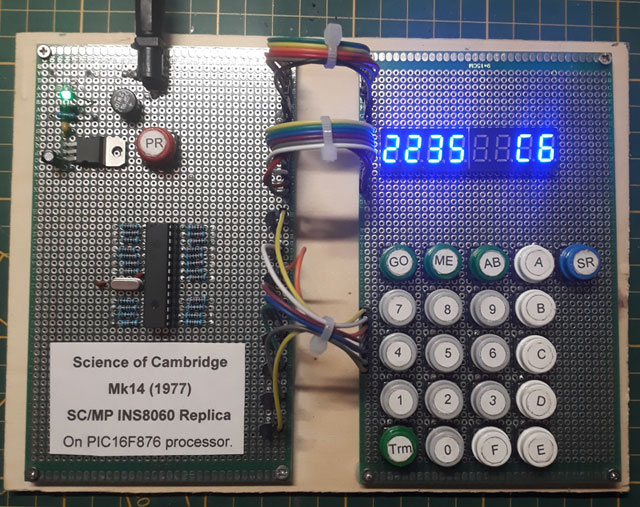
This page is dedicated to the MK14 clone using a PIC processor, the PIC14. When I was 13 years old I read a lot about the INS8060, also called the SC/MP processor. I didn’t have much money and I could barely afford to buy an electronics magazine called Elektor every month, and they published a simple computer board based on the SC/MP processor. I read everything I could about the SC/MP processor. Since I didn’t have the money to buy a real processor I drew the inside of the processor on a big piece of paper, together with the RAM/ROM/keyboard and display as registers and I had lots of little zero and one papers to control the flow of the bits and bytes on the (paper) circuit. Looking back, this was ridiculous, but that’s how I learned computer design and binary logic. At the time there was also a board called the MK14 also based on the SC/MP processor and I considered buying one at the time. Now that I have enough money and time, the INS8060 processor is no longer for sale (at least not at a reasonable price). This page shows an MK14 emulation using a PIC processor called PIC14, which behaves exactly like an original MK14 in terms of hardware. With a little soldering skills it can be built in a few evenings. If you want to know more about the INS8060 or the SC/MP processor, you can look at my English page about this processor.
Here you see the version I made myself, on one PCB is the power supply and the processor, on the other the keyboard and the display. I’ve set everything up very broadly so that it would be easier to create (and debug in case of an error). The whole is mounted on a wooden plate so that it can stand in the display cabinet and is stable for use.

This is the schematic, all details and building instructions, including the code for the PIC processor can be found on the website Karen’s Corner http://techlib.com/area_50/Readers/Karen/micro.htm#PIC1
Another PIC14
An acquaintance from the UK sent me a PCB for a PIC14 clone that uses a UN2003 transistor array IC and has a nice compact setup. This one is also based on Karen’s original design. I had all the parts in stock so on a drizzly Saturday evening it was put together in a few hours.

Yet another PIC14
If you want to build a PIC14 yourself and do not want to wire it on an experiment board, it is difficult to find another PCB. The Dutch company Budgetronics.eu supplies a complete kit that is also based on Karen’s design at a reasonable price.

You can order the kit at: https://www.budgetronics.eu/nl/bouwpakketten/cambridge-mk14-in-a-pic-computer-bouwkit/a-25922-20
Original MK14

This is the original version of the MK14 single board computer, it was not an Acorn product but a first step in the creation of Acorn Computers. Chris Curry worked with Clive Sinclair on the development of the MK14 as a Science of Cambridge/Sinclair product. The MK14 was made by Science of Cambridge (later Sinclair Computers and
finally Sinclair Research). The MK14 was based on the National Semiconductors SC/MP (INS8060) processor and was sold as a kit. It could be programmed for a built-in monitor program and the hexadecimal keyboard and seven-segment displays.
Links
Tech info Nintendo NES

The NES CPU was a (customized) 6502 8-bit (NMOS) processor at 1.79 Mhz, this was a dedicated chip, but nowedays you can buy this custom chip in China. The internal memory consisted of 2 Kbytes of ram and the system also had 2 Kbytes of video ram. The video resolution is 256 x 240 pixels with a total of 52 colors of which 24 can be used simultaneously. The sprite engine supported a maximum of 64 sprites with a resolution of 8 x 16 pixels. The maximum size of a cartridge was 4 megabits. The NES also had its own sound chip with which the typical NES sound was made. Who does not know the typical sounds of the Mario game. On this page you can find the electronics schematics of the NES console, on the page they are reduced displayed, when you save these electronics schematics on your own computer by means of the right mouse button you will download them in large format.

Nintendo’s origins date back to 1889 with the making of playing cards, where they became quite big. In 1963 they also
started making games in addition to playing cards. In 1970, Nintendo stopped making playing cards and by then they
focused on making toys. In July 1983 they released their first own game console, the Famicom with games like Donkey Kong, Donkey Kong Jr and Popeye as launch titles. By the end of the year the Famicom’s game collection consisted of a lot of games including Mario Bros. Nintendo didn’t have any third-party software developers and sold over a million Famicom systems, proving the powerb of their own software. Nintendo decided in 1985 that it was necessary to adjust the design of the Famicom. The console took the form of a simple box with two controller ports and a slot to insert the game cartridge. The game console was renamed to Nintendo Entertainment System (NES). The original NES package, which was released as a test in New York City during the fall of 1985, contained two controllers, an adapter and cables to connect it to the television. Super Mario Bros became a big hit, selling a million copies.
The Nintendo NES was also the first real game console we bought for my kids and we spent hours watching our oldest son playing Super Mario on the Nintendo NES on the living room television set. Since I have an electrical engineering background, the first adjustment (undoing the region code) quickly done and knew what was inside the Nintendo NES. One of my sons has another Nintendo NES and even my youngest daughter also enjoyed the games. I think it’s partly because the graphic possibilities weren’t that great, the makers had to make sure the game was super well put together. Nowadays I often notice that the quality of the graphics is great but that this has come at the expense of the story and the game line. Since the Nintendo NES hardware was fairly simple, there are quite a few emulators and Nintendo NES games can be played on almost any platform. A few years ago I made Nintendo NES case console by means of a Raspberry Pi a complete with hundreds of games on board. This page is about the Nintendo NES and everything I’ve collected about this over the past few years.
Specifications of a Nintendo NES gamecomputer
- CPU type: modified 6502 8-bit (NMOS)
- CPU speed: 1.79 Mhz
- RAM memory: 16 Kbit (2 Kbyte)
- Video RAM: 16 Kbit (2 Kbyte)
- Picture resolution: 256×240 pixels
- Colors Available: 52 colors
- Max colors at once: 24 colors
- Max sprite size: 8×16 pixels
- Max sprites: 64 sprites
- Min/Max Cart Size: 128 Kbit – 4 Mbit
- Max sprites per Scanline: 8 sprites
- Sound: PSG sound
The NES CPU was a (customized) 6502 8-bit (NMOS) processor at 1.79 Mhz, this was a dedicated chip, but nowedays you can buy this custom chip in China. The internal memory consisted of 2 Kbytes of ram and the system also had 2 Kbytes of video ram. The video resolution is 256 x 240 pixels with a total of 52 colors of which 24 can be used simultaneously. The sprite engine supported a maximum of 64 sprites with a resolution of 8 x 16 pixels. The maximum size of a cartridge was 4 megabits. The NES also had its own sound chip with which the typical NES sound was made. Who does not know the typical sounds of the Mario game.
Schematics of the NES
Here are the electronics schematics of the NES console, on the page they are reduced displayed, when you save these electronics schematics on your own computer by means of the right mouse button you will download them in large format.


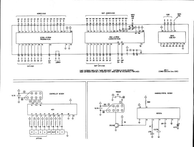
Information about the Catridge pinout
NES MASK ROM Pinouts:
---------------------------------------------
PRG ROM - 32KBytes (28pin):
(no need to change any pins on EPROM)

                  ---_---
       +5V     - |01   28| - +5V
       PRG A12 - |02   27| - PRG A14
       PRG A7  - |03   26| - PRG A13
       PRG A6  - |04   25| - PRG A8
       PRG A5  - |05   24| - PRG A9
       PRG A4  - |06   23| - PRG A11
       PRG A3  - |07   22| - PRG /CE
       PRG A2  - |08   21| - PRG A10
       PRG A1  - |09   20| - GND
       PRG A0  - |10   19| - PRG D7
       PRG D0  - |11   18| - PRG D6
       PRG D1  - |12   17| - PRG D5
       PRG D2  - |13   16| - PRG D4
       GND     - |14   15| - PRG D3
                  -------

---------------------------------------------
PRG ROM - 128KBytes (28pin):

                  ---_---
       PRG A15 - |01   28| - +5V
       PRG A12 - |02   27| - PRG A14
       PRG A7  - |03   26| - PRG A13
       PRG A6  - |04   25| - PRG A8
       PRG A5  - |05   24| - PRG A9
       PRG A4  - |06   23| - PRG A11
       PRG A3  - |07   22| - PRG A16
       PRG A2  - |08   21| - PRG A10
       PRG A1  - |09   20| - PRG /CE
       PRG A0  - |10   19| - PRG D7
       PRG D0  - |11   18| - PRG D6
       PRG D1  - |12   17| - PRG D5
       PRG D2  - |13   16| - PRG D4
       GND     - |14   15| - PRG D3
                  -------

----------------------------------------------
PRG ROM - 256KBytes (32pin):

                  ---_---
       PRG A17 - |01   32| - +5V
       PRG /CE - |02   31| - +5V
       PRG A15 - |03   30| - +5V
       PRG A12 - |04   29| - PRG A14
       PRG A7  - |05   28| - PRG A13
       PRG A6  - |06   27| - PRG A8
       PRG A5  - |07   26| - PRG A9
       PRG A4  - |08   25| - PRG A11
       PRG A3  - |09   24| - PRG A16
       PRG A2  - |10   23| - PRG A10
       PRG A1  - |11   22| - PRG /CE
       PRG A0  - |12   21| - PRG D7
       PRG D0  - |13   20| - PRG D6
       PRG D1  - |14   19| - PRG D5
       PRG D2  - |15   18| - PRG D4
       GND     - |16   17| - PRG D3
                  -------

(note: pins 2 and 22 are connected together on the PCB)

----------------------------------------------
PRG ROM - 512KBytes (32pin):

                  ---_---
       PRG A17 - |01   32| - +5V
       PRG A18 - |02   31| - +5V
       PRG A15 - |03   30| - +5V
       PRG A12 - |04   29| - PRG A14
       PRG A7  - |05   28| - PRG A13
       PRG A6  - |06   27| - PRG A8
       PRG A5  - |07   26| - PRG A9
       PRG A4  - |08   25| - PRG A11
       PRG A3  - |09   24| - PRG A16
       PRG A2  - |10   23| - PRG A10
       PRG A1  - |11   22| - PRG /CE
       PRG A0  - |12   21| - PRG D7
       PRG D0  - |13   20| - PRG D6
       PRG D1  - |14   19| - PRG D5
       PRG D2  - |15   18| - PRG D4
       GND     - |16   17| - PRG D3
                  -------

---------------------------------------------
CHR ROM - 32KBytes (28pin):
(no need to change any pins on EPROM)

                  ---_---
       +5V     - |01   28| - +5V
       CHR A12 - |02   27| - PRG A14
       CHR A7  - |03   26| - PRG A13
       CHR A6  - |04   25| - CHR A8
       CHR A5  - |05   24| - CHR A9
       CHR A4  - |06   23| - CHR A11
       CHR A3  - |07   22| - CHR /RD  (OE)
       CHR A2  - |08   21| - CHR A10
       CHR A1  - |09   20| - CHR /A13 (CE)
       CHR A0  - |10   19| - CHR D7
       CHR D0  - |11   18| - CHR D6
       CHR D1  - |12   17| - CHR D5
       CHR D2  - |13   16| - CHR D4
       GND     - |14   15| - CHR D3
                  -------

----------------------------------------------
CHR ROM - 128KBytes (32pin):

                  ---_---
       +5V     - |01   32| - +5V
  (OE) CHR /RD - |02   31| - CHR /A13 (CE)
       CHR A15 - |03   30| - +5V
       CHR A12 - |04   29| - CHR A14
       CHR A7  - |05   28| - CHR A13
       CHR A6  - |06   27| - CHR A8
       CHR A5  - |07   26| - CHR A9
       CHR A4  - |08   25| - CHR A11
       CHR A3  - |09   24| - CHR A16
       CHR A2  - |10   23| - CHR A10
       CHR A1  - |11   22| - GND
       CHR A0  - |12   21| - CHR D7
       CHR D0  - |13   20| - CHR D6
       CHR D1  - |14   19| - CHR D5
       CHR D2  - |15   18| - CHR D4
       GND     - |16   17| - CHR D3
                  -------

----------------------------------------------
CHR ROM - 256KBytes (32pin):

                  ---_---
       CHR A17 - |01   32| - +5V
  (OE) CHR /RD - |02   31| - CHR /A13 (CE)
       CHR A15 - |03   30| - +5V
       CHR A12 - |04   29| - CHR A14
       CHR A7  - |05   28| - CHR A13
       CHR A6  - |06   27| - CHR A8
       CHR A5  - |07   26| - CHR A9
       CHR A4  - |08   25| - CHR A11
       CHR A3  - |09   24| - CHR A16
       CHR A2  - |10   23| - CHR A10
       CHR A1  - |11   22| - GND
       CHR A0  - |12   21| - CHR D7
       CHR D0  - |13   20| - CHR D6
       CHR D1  - |14   19| - CHR D5
       CHR D2  - |15   18| - CHR D4
       GND     - |16   17| - CHR D3
                  -------

----------------------------------------------
WRAM - 8KBytes (28pin):

                  ---_---
       +5V     - |01   28| - +5V
       PRG A12 - |02   27| - WRAM /WE
       PRG A7  - |03   26| - WRAM /CE
       PRG A6  - |04   25| - PRG A8
       PRG A5  - |05   24| - PRG A9
       PRG A4  - |06   23| - PRG A11
       PRG A3  - |07   22| - GND
       PRG A2  - |08   21| - PRG A10
       PRG A1  - |09   20| - WRAM /CE
       PRG A0  - |10   19| - PRG D7
       PRG D0  - |11   18| - PRG D6
       PRG D1  - |12   17| - PRG D5
       PRG D2  - |13   16| - PRG D4
       GND     - |14   15| - PRG D3
                  -------
Additional information about the roms and the memory mapper
Description how to disable the “lockout chip” on the NES.
When nintendo designed the Nes they put a so-called lockout chip in to make sure that only licensed companies could release games for the NES and they could also use region codes so that USA cartridges would not work on European NES systems. It worked like this, the lockout chip was in the console as well as the cartridge and when the NES was turned on, the chip from the console will communicate with the chip in the cartridge. If the codes did not match, the chip would reset the NES every second. However simply cutting one pin of the chip could undo this protection.
DIY Intel 8052 Basic computer
A while ago I bought an old box with integrated circuits that had been stored for many years and contained a lot of tubes with very old IS’s. As I like to build old processor boards and try to repair old computers and boards, these chips were very welcome. In one tube there were two original P8052-Basic chips and that brought back good memories of the time mid 80ties of last century when I was working as head R&D embedded programmer and hardware designer for a small company and was using the 8031 processor a lot. I even extended a tiny Basic version at that time, but the real P8031-Basic was incredible and complete, but expensive and hard to get at that time. I put these chips in my computer chips and cpu collection and one I kept aside to make a board to get it working again.

I had a latch and a memory chip in my workshop, a PCB was also there, I only needed to order a few 11.0592 crystals as these are not so common anymore. After two evenings of wiring it was finally ready and at my first attempt to run it I got a line number error all the time. I seemed that the external sram was not working and it was a small wiring error.

After I had fixed that it worked like a charm, I connected it to my VT100 terminal with the TTL serial input and after pressing the spacebar I got the prompt and I could write a small Basic program. On this page I will show you the schematic I made, some build instructions and some documentation and (source)code.

https://www.heinpragt-software.com/software_development/8052_processor_ide.html
AT89C52 – Basic
The INTEL 8052AH-BASIC is not available anymore and very rare, I have tried to put the code into a AT89C52 processor and after a few tries this worked fine. You can order a AT89C52 with the service that I will pre program the chip. https://www.heinpragt.nl/?product=at89c52-basic
Links and downloads
- https://www.heinpragt-software.com/software_development/Intel_8052_basic_computer.html
- The Microcontroller Idea Book – Circuits and programs for the 8052-BASIC Microcontroller – Jan Axelson.
- The Microcontroller Idea Book – examples Disk
- P8052_Basic datasheet.pdf
- STC89Cxx_datasheet.pdf
- BAS52 Manual.
- The original Zip file with the sourcecode of the Basic52 interpreter from Intel.
Z80 Arduino mega board

I found an interesting project on the Internet of a Z80 processor on a breadboard that was connected with wires to an Arduino Mega board. It had some code with it, it was far from complete but it triggered me. I adopted the idea and improved it, rewrote the Arduino code and improved the hardware design. The Z80 processor in this project is running at 200 Khz, clocked from the Arduino and the Arduino emulates 8 kb of ROM and 6 kb of RAM and serial input and output. With this simple and cheap configuration you have a complete working Z80 based computer. With some adjustments I even got a complete Basic interpreter running on this hardware with the serial I/O of the Arduino as interface. But it is also nice to write your own assembler code and see it not only running in an emulator, but also on a real Z80 processor. Just put your generated HEX code in the memory.h file and recompile the Arduino sketch and upload it to the Mega board. On reset the Z80 will execute the code in the ROM section of the MEGA. Have fun!
https://www.heinpragt-software.com/software_development/z80_arduino_mega_project.html
Z80 processor information

This is a page about my first favorite microprocessor that I worked with, the Z80 processor. When I was twenty years old in 1979 I bought my first real computer, the Tandy TRS-80 model I level II with a Z80 processor at its heart. In no time I was able to program in assembler for this and I wrote complex assembler programs and utilities for the Z80 processor. All computers I bought after that had a Z80 processor like the Sinclair Spectrum and later the MSX. After My first job was developing hardware and software on embedded Z80 systems (cash register and machine control systems) in assembler and PL/Z. After that I started working at Micro Technology (an MSX hardware supplier) and again I was programming assembler using the Z80 but the I also learned to program in ‘C’. After that the 8031 processor became my second love and I then I started to write assembly for the 8086 and 80186 processor. I have been an embedded programmer until 1999 when I switched to Internet programming. After many years I picked up the Z80 again and on this page you can find information about old and new Z80 projects and find the documentation. The Z80 was a genius design for its time and its funny that this processor is still used and available.
Regards, Hein Pragt.
I also have a Facebook Group on Retro Computing and Electronics, feel frtee to join!
About the Zilog Z80

The Z80 was developed by Federico Faggin who had been working at Fairchild Semiconductor and later at Intel on fundamental transistor and semiconductor manufacturing technology. He had been working on the Intel 4004 and 8080 processor and several other ICs. Masatoshi Shima, the principal logic and transistor level-designer of the 4004 and the 8080. The first working samples of the Z80 processor were delivered in March 1976, and it was officially introduced on the market in July 1976. They also developed assembler based development systems and some peripheral ICs to build computer systems with a low number of chips. A good move was that Faggin designed the instruction set to be binary compatible with the Intel 8080 processor so that most 8080 code would run unmodified on the new Z80 CPU. But he Z80 had a lot of extensions to the 8080 processor and became very popular. A lot of companies took a license and the Z80 processor (and support chips) were manufactured by many companies. Beside the single 5V power the built-in DRAM refresh that made computer systems cheaper with larger memory because dynamic ram chips were much simpler, a lot of ram element could be packed in a single chip and the price per bit was very low compared to static ram chips.
Z80 40 pins DIL pins
The most handy version of the Z80 processor to me is still the 40 pins DIL Z80 version, it’s easy to solder into a board and the pins are big enough for the clips of measuring devices.

Z80 pin functions
- A15–A0. Address Bus (output, active High, tristate). A15–A0 form a 16-bit Address Bus, which provides the addresses for memory data bus (up to 64 KB) and for I/O device addressing.
- BUSACK. Bus Acknowledge (output, active Low). Bus Acknowledge indicates to the requesting device that the CPU address bus, data bus, and control signals MREQ, IORQ, D, and WR have entered their high-impedance states. The external circuitry can now control these lines.
- BUSREQ. Bus Request (input, active Low). BUSREQ forces the CPU address bus, data bus, and control signals MREQ, IORQ, RD, and WR to enter a high-impedance state so that other devices can control these lines. BUSREQ is normally wired OR and requires an external pull-up for these applications.
- HALT indicates that the CPU has executed a HALT instruction and is waiting for either a nonmaskable or a maskable interrupt (with the mask enabled) before operation can resume. During HALT, the CPU executes NOPs to maintain memory refreshes.
- INT. Interrupt Request (input, active Low). An Interrupt Request is generated by I/O devices. The CPU honors a request at the end of the current instruction if the internal software-controlled interrupt enable flip-flop (IFF) is enabled.
- D7–D0. Data Bus (input/output, active High, tristate). D7–D0 constitute an 8-bit bidirectional data bus, used for data exchanges with memory and I/O.
- IORQ. Input/Output Request (output, active Low, tristate). IORQ indicates that the lower half of the address bus holds a valid I/O address for an I/O read or write operation. IORQ is also generated concurrently with M1 during an interrupt acknowledge cycle to indicate that an interrupt response vector can be placed on the data bus.
- M1. Machine Cycle One (output, active Low). M1, together with MREQ, indicates that the current machine cycle is the op code fetch cycle of an instruction execution. M1, when operating together with IORQ, indicates an interrupt acknowledge cycle.
- MREQ. Memory Request (output, active Low, tristate). MREQ indicates that the address bus holds a valid address for a memory read or a memory write operation.
- NMI. Nonmaskable Interrupt (input, negative edge-triggered). NMI contains a higher priority than INT. NMI is always recognized at the end of the current instruction, independent of the status of the interrupt enable flip-flop, and automatically forces the CPU to restart at location 0066h.
- RD. Read (output, active Low, tristate). RD indicates that the CPU wants to read data from memory or an I/O device. The addressed I/O device or memory should use this signal to gate data onto the CPU data bus.
- RESET. Reset (input, active Low). RESET initializes the CPU, during reset time, the address and data bus enter a high-impedance state, and all control output signals enter an inactive state. RESET must be active for a minimum of three full clock cycles before a reset operation is complete
- RFSH. Refresh (output, active Low). RFSH, together with MREQ, indicates that the lower seven bits of the system’s address bus can be used as a refresh address to the system’s dynamic memories.
- WAIT. input, active Low). WAIT communicates to the CPU that the addressed memory or I/O devices are not ready for a data transfer. The CPU continues to enter a WAIT state as long as this signal is active.
- WR. Write (output, active Low, tristate). WR indicates that the CPU data bus contains valid data to be stored at the addressed memory or I/O location.
- CLK. Clock (input). Single-phase MOS-level clock.
The Zilog Z80 CPU is a fourth-generation enhanced microprocessor, the internal registers include two sets of six general-purpose registers which can be used individually as either 8-bit registers or as 16-bit register pairs. In addition there are two sets of Accumulator and Flag registers. The Z80 CPU also contains a Stack Pointer, Program Counter, two index registers, a refresh register, and an interrupt register. The CPU only requires a single +5V power source. All output signals are fully decoded and timed to control standard memory or peripheral circuits. This figure shows the internal
architecture and major elements of the Z80 CPU.

The Z80 CPU contains 208 bits of read/write memory that are implemented using static RAM. This memory is configured to eighteen 8-bit registers and four 16-bit registers. The registers include two sets of six general-purpose registers that can be used individually as 8-bit registers or in pairs as 16-bit registers. There are also two sets of Accumulator and Flag registers and six special-purpose registers. The first special purpose register is the Program Counter (PC). The program counter holds the 16-bit address of the current instruction being fetched from memory. The Program Counter is automatically incremented after its contents are transferred to the address lines. When a program jump occurs, the new value is automatically placed in the Program Counter. The second special purpose register is the Stack Pointer (SP). The stack pointer holds the 16-bit address of the current top of a stack located anywhere in the system RAM memory. The stack organized as a last-in first-out (LIFO) file. Data can be pushed onto the stack from specific CPU registers or popped off of the stack to specific CPU registers through the execution of PUSH and POP instructions. The data popped from the stack is always the most recent data pushed onto it.

The third pair of special purpose registers are the two Index Registers (IX and IY). The two independent index registers hold a 16-bit base address that is used in indexed addressing modes. In this mode, an index register is used as a base to point to a region in memory from which data is to be stored or retrieved. An additional byte is included in indexed instructions to specify a displacement from this base. The fourth special purpose register is the Interrupt Page Address (I) Register. The Z80 CPU can be operated in a mode in which an indirect call to any memory location can be achieved in response to an interrupt. The I register is used for this purpose and stores the high-order eight bits of the indirect address while the interrupting device provides the lower eight bits of the address. The fifth special purpose register is the Memory Refresh (R) Register. The Z80 CPU contains a memory refresh counter, enabling dynamic memories to be used with the same ease as static memories. Seven bits of this 8-bit register are automatically incremented after each instruction fetch, the data in the refresh counter is sent out on the lower portion of the address bus along with a refresh control signal while the CPU is decoding and executing the fetched instruction. The last pair of special purpose registers are the Accumulator and Flag Registers. The CPU includes two independent 8-bit Accumulators and associated 8-bit Flag registers. The Accumulator holds the results of 8-bit arithmetic or logical operations while the Flag Register indicates specific conditions for 8-bit or 16-bit operations, such as indicating whether or not the result of an operation is equal to zero. The programmer selects the Accumulator and flag pair with a single exchange instruction.
There are also two sets of General Purpose Registers, each containing six 8-bit registers that can be used individually as 8-bit registers or as 16-bit register pairs. One set is called BC, DE, and HL while the complementary set is called BC’, DE’, and HL’. At any one time, the programmer can select either set of registers to work through a single exchange command for the entire set. This can be used in and interrupt routine to use the alternate register set and switch back at the end instead of pushing all registers to stack and restoring them afterwards. This is sacrificing a complete set of registers in favor of speed. The Arithmetic Logic Unit can execute 8 bit arithmetic and logical instructions. Internally, the ALU communicates with the registers and the external data bus by using the internal data bus. Functions performed by the ALU include: Add, Subtract, Logical AND, Logical OR, Logical exclusive OR, Compare, Left or right shifts or rotates, Increment, Decrement, Set bit, Reset bit and Test bit.
Z80 Timing
The next diagram describes the pins and signal timings the Z80 takes to get data from memory, or store it into memory or IO. These transfer of address and data occurs parallel and is based on how memory chips work with their CS, OE, and WR signals. The image below shows the data, timing and sequence of all pins involved.
When the Z80 is reset it begins by reading the first instruction in memory at address location 0x0000. To fetch the instruction, the Z80 starts by setting the address pins to 0x0000, and then sets M1 to low. On the falling edge of the first clock pulse, the Z80 sets the RD pin to low to indicate that it wants to read data, while the MREQ pin goes low to indicate that the Z80 wants to read data from memory. The next clock cycle, T2, is an extra delay cycle that gives external memory time to produce its output. On the third clock cycle the Z80 reads the data in from the data pins, and on the rising edge of the third clock cycle the Z80 resets the RD and MREQ pins back to high. The data that was read will be an instruction, and the Z80 will either execute the instruction or get more data from memory to complete the instruction.
When the Z80 wants to write to memory, it first sets the address pins to the location it wants to write to. On the falling edge of the first clock, the MREQ pin is set to low to indicate that it wants to write to memory, and the data pins are set to the data that has to be saved. On the falling edge of the second clock, the Z80 sets the WR pins to low to signal to the I/O device or memory that the data is valid to copy into the memory chip that has been selected. On the falling edge of the third clock cycle, the Z80 sets WR and MREQ to high to indicate the ending of the write cycle.
In I/O instructions the Z80 does the same, but uses IORQ instead of the MREQ pin.
As you can see the Z80 processor is very easy in timing and a very friendly CPU to all kind of computer chips. The timing diagrams are also very logic and require a minimal number of external chips to build a complete system. I will not discuss the timing diagrams here, they can be found in the Z80 manual. What I can show is a minimal Z80 system with a CPU some ROM (EPROM) and static RAM memory and a serial I/O port. This minimal system can still be bought for somewhere between 25 and 35 euros. It usually comes with a build in Basic interpreter, but I delete that and the fun part is making your own system from scratch in assembler or ‘C’.
Z80 with atmega chip as I/O and memory
Because the easy and logical signal timings of the Z80 processor a complete Z80 system can be build using a Atmega processor to emulate the ROM, the RAM, the clock signal and the I/O for the Z80 processor. There are several projects today that use this concept, the easiest one is a simple project using a Z80 processor and an Arduino Mega board. The Arduino Mega board is fast enough to provide the correct I/O timing and emulate a ROM and RAM chip in the internal memory of the Arduino Mega. The Serial I/O is also handled the Arduino Mega, to the Z80 it’s just an I/O port. Just include the Z80 code as hex array in the include file. My Z80 IDE software can generate this ‘C’ style hex array. You can develop test and debug the code in my Z80 IDE and then see the code running on a real Z80 CPU.

This is the schema of all the connections of the Z80 pins to the Arduino Mega board I/O pins.

Beacuse this is a rather fragile solution I build this project on am Arduino Mega experriment shield, using a IC socket for the Z80 and a pin array on both sides to connect the pins of the Z80 to the Arduino Mega pins. I could also use shorter wires and the whole shield is more permanent and reusable.

You can use the Arduino IDE to upload new Z80 code the Arduino Mega time after time and use the build in terminal as serial I/O of the Z80 processor. You can find the original project, schematics and source code on this site. The project on Arduin project hub.
And here is anothe project using the same idea: Site of Baltazar Studios.
Z80 MBC computer board
Another nice project that’s currently in version 3 is the Z80-MBC project. Currently version 3 is very sophisticated and becoming a real computer, I like the smaller version the Z80-MBC2 and even the original Z80-MBC. Version 2 is a very easy to build Z80 Single Board Computer with a SD as “disk emulator” and with a 128KB banked RAM for CP/M 3 (but it can run CP/M 2.2). It has an optional on board 16x GPIO expander, and uses common cheap add-on modules for the SD and the RTC options. It also has an “Arduino heart” using an Atmega32A as EEPROM and “universal” I/O emulator (like the Arduino Mega board in the above project) although it’s a little harder to find a programmed Atmega32A because this chip can only be programmed using an ISP programmer. But you can buy this computer board as a complete kit on the Internet. You can use the programming tools of CP/M, but this acts more like a real Z80 full computer system. But it is still low cost (around 70 euro) and a nice way to see what programming was like in the “old days”.

You can download and read all the source code, the schematics and build instructions on the project site. Go to project page on hackaday.io website.
As you can see there is still an active community building nice projects using the good old Z80 CPU. The Z80 CPU and all the chips are still available and the DIL (Dual in line) versions are easy the handle and to solder into a circuit The Z80 was my first love (for a CPU) and it will remain my favorite processor.
Z80 PIO chip
In a lot of Z80 based systems you can see the Z80 PIO chip beside the Z80 CPU chip. This chip is basically just a digital parallel I/O port chip. You can configure the individual port pins as digital inputs or outputs and then use them for whatever you want. The A/B input selects between either PortA or PortB and the C/D input selects between either the control register or the data register. The control registers are used to configure the ports and the data registers are used to read/write the actual data. By connecting these to A0 and A1 one can access the desired register using the address bus in an I/O read or write. The least significant bit of the memory address A0 then seledts the port A or B and the A1 line selects between the data and the control registers. With an address decoder you can put this chip anywhere in the I/O addressing space. In a lot of systems this chip was used to add a parallel printer port to the Z80 system. But the chip can also handle digital inputs from switches and can be used to driver signaling LEDs. One of the unique features of the Z80-PlO is that all data transfer between the peripheral device and the CPU can be accomplished under total interrupt control even with nested interrupts. The the PlO can be programmed to interrupt if any specified peripheral alarm conditions should occur. This interrupt capability reduces the amount of time that the processor has to spend in polling peripheral status.You can still buy this chip and it costs only a few dollars.

The Z80 PIO Pins.

Link to documentation: z80piomn.pdf Z80 PIO User Manual (Pdf).
Z80 SIO chip
Beside the parallel PIO chip there was also a SIO chip for serial communication. Unfortunately this was a complicated chip to program and I do not see it used nowadays. The SIO contains 3x READ ONLY registers for the ‘B’ channel, 2x READ ONLY registers for the ‘A’ channel, 8x WRITE registers on the ‘B’ channel and 7x WRITE registers for the ‘A’. Clearly for anyone attempting to make one of these things work correctly, a degree of understanding is needed. The device can be used in polling mode and also in interrupt mode when a character us received or and output buffer is empty. With other registers you can set or read the additional control lines. I never used this device and nowadays there are several alternative chips available.
The Z80 SIO internal.

The S80 PIO Pins.

Link to documentation: ps0183.pdf Z80 SIO Manual (Pdf).
The Z80 actually has a 4-bit ALU
 As you can read on other pages, I am a reasonable fan of the Z80 processor. The Z80 is officially an 8 bit processor but also has registers that can be used as a pair as a 16 bit register. That’s why I was surprised to read that the Z80 actually has a 4-bit ALU (Arithmetic logic unit). How that works I try to explain on this page. The makers of the Z80 are already dropping something about this in a interview of the computer history museums. I also think that Ken Shirriff in his blog here excellent explains thie feature.
Some fanatics have been studying the Z80’s silicon to understand the processor’s physical layout. The ALU of the Z80 exists of four one-bit ALU units that together form a four-bit ALU. The ALU itself has a 4 bit high bit bus and a four bit low bit bus.

An operation starts by loading 2 oparands from the registers to the four bit latches. What I didn’t draw here is that bit shift is already happening when loading this operations can be performed. Then via the two four-bit mux (multiplexers) of both op1 and op2 the lowest four bits will pass through the ALU and be stored in the low bit latch. Then the high four bits will be presented to the ALU via the multiplexers and the result is low together with the stored four bits. latch again a 2 x 4 = 8 bit value that can be written back to the result register.
I have simplified this diagram a bit, in reality there are two shifters between the register bus and the 4 bit buses of the ALU, which both move to can slide left and right and there are inverters for the MUX to simplify calculations. There is also logic for the carry and the other flags in, but since these don’t make any difference to the principle, I’ve left them out. This also explains the so-called half carry of the Z80 processor. The 4 bit ALU can perform operations on two times four bits such as addition, subtraction, logical AND / OR and XOR. Together with the bit shifters, this allows all operations are performed. This also explains why certain operations also cost so many cycles.
Why did they choose a 4 bit CPU instead of a full 8 bit CPU? The first reason I could think of is a simpler design, but if you think carefully this will not really be the case. The real reason is in the interview. Since both designers came from Intel and the 8080 had worked and the Z80 would be byte compatible (and thus a direct replacement without code changes) were lawsuits from Intel lurking of course. So it was important to make a design that would deviate so much from the 8080 design, but with exactly the same functionality. Some changes in the design of the transistors on the silicon were just real improvements but the structure of the CPU was so completely different so this was a deliberate action to avoid lawsuits from Intel.
Conversely, Zilog also ran the risk that companies such as NEC would copy their new processor and for that, silicon design a number of “traps”. These were transitors that had no function or affect the design, but were only meant to make reverse engineering more difficult. Apparently NEC later admitted that they were delayed by six months because of these traps.
There was one thing that Intel really had a patent on and that was the set of menomics (short for the names of the instructions) so Zilog had to build a completely new set of instruction names. Intel later carried over their instruction names in all new processors and so did Zilog. This was sometimes difficult for programmers, especially when one had to program for both the 8080 and the Z80. I had to do this myself too. But since I have processors for many differences programmed in assembler I learned to keep the different sets of instructions apart.
Freeware Z80 IDE
To be able to program for the z80 you need an assembler or compiler. I personally still like to write in Z80 assembler but I could no longer find tools for Windows 10. There were still some programs to download but most of them worked at DOS level. After some searching I decided that it was time for a new hobby project, building a complete integrated Z80 development environment. I found a pretty good assembler and good portable C code from an emulator and the rest I had somewhere in my code library. The result is Z80 workbench, a portable x64 Windows program that includes an editor, assembler, disassembler, emulator, single step debugger, Intel hex read / write function a terminal window, an MPF-1 compatible seven segment display with 8 LEDs and keyboard support. One of the unique features of the Z80-PlO is that all data transfer between the peripheral device and the CPU can be accomplished under total interrupt control even with nested interrupts. The the PlO can be programmed to interrupt if any specified peripheral alarm conditions should occur. This interrupt capability reduces the amount of time that the processor has to spend in polling peripheral status. Download the program on this page
Z80 related documents
- z80.info/zip/z80cpu_um.pdf Z80 Family CPU User Manual (Pdf).
- Zilog_z80_manual.pdf Another Z80 CPU User Manual (Pdf).
- How to program the Z80 by Rodnay Zaks (pdf) The best book on the Z80 ever, I used it for many years.
- Z80-CPU%20Technical%20Manual.PDF Z80 technical manual (pfd).
- MPF-I-User’s-manual.pdf Old Z80 based board, the MPF-I.
- Sams ComputerFacts – Model I (1985)(Howard Sams)(pdf)
- Radio Shack TRS-80 Micro Computer Technical Reference Handbook 2nd
- Expansion Interface Service Manual (19xx)(Radio Shack)(pdf)
- Download Game BoyTM CPU Manual!
Z80 links, tips and webpages
- Wikipedia Z80 page A very complet and intersting page about the Z80 processor.
- github.com/WestfW/4chipZ80 Code and design of a 4 Chip Z80 computer board.
- http://map.grauw.nl/resources/z80instr.php An overview of the Z80 instruction set.
- jorgicor.sdfeu.org/uz80as/ Sources and binaries of uz80as, a cross assembler for the Zilog Z80 microprocessor.
- github.com/anotherlin/z80emu Portable C sourcode of a good Z80 emulator.
- Programmeren_in_TI-83_plus_Assembly TI 83 Plus Z80 Assembly Programming
My first real Z80 computer the TRS80 Model 1
This was my first real computer back in the 80ties and I wrote a lot software for this computer in basic but also a lot in assembler. I expanded the memory myself by piggybacking the 64K dynamic RAM chips on top of the 16K versions and I expanded the video circuit to lowercase as well. I did several other upgrades and by the time I switched to a Sinclair spectrum the TRS80 was full of wires and mods, but still running fine. I lost that computer in one of the moves I did to another house, it is still sad I lost it. Using this computer I learned the Z80 processor inside out.
- Name: TRS 80 Model I
- Company: Tandy Radio Shack
- Made in: U.S.A.
- Year: 1977
- Basic: Level II (12k ROM models)
- Keyboard: Full 53 keys
- CPU: Zilog Z80 / 1.77 MHz
- RAM: 4 kb / 16 kb
- VRAM: 1 kb
- ROM: 12kb (Basic Level 2)
- Textmode: 32 x 16 of 64 x 16
- Graphics: 128 x 48 pixels
- Color: None (B/W)
- Sound: None
- I/O: Monitor, cassette interface, expansion port
TRS80 Model 1 documents
HeinPragt.com software development. (Eng)
On these pages you can find a list of my applications, instructions and documentation and links to download or buy the applications. Most of these (utility) programs were developed out of my own needs, because something was not available at that time, or I was not satisfied with the current solutions available. Most of these programs are Freeware, you can download them from this website. I like portable programs that do not need am installer, but sometimes an installer is needed. I will keep things as clean as possible and never leave files behind. These programs are written in C, C++ or C# and all executables are digitally signed with my company code signing certificate for safety.
All articles on the website: www.heinpragt-software.com
- 6502 processor IDE
- 8052 processor IDE
- Adventure interpreter
- Amerwold woods
- Apple 1 emulator
- Arduino RFID Door Lock
- Arduino Scrolling Led Display
- Bon Vivant
- CpmBox a CPM 2.2 emulator
- ESP32 based WIFI internet radio
- ESP8226 WIFI led control
- Game programming
- hmpFileFind utility
- Http health check monitor
- INS8060 or scmp processor
- Intel 8052AH Basic computer
- MC14500B processor IDE
- Minimal Emulator Frontend
- MK14 emulator
- MPF-1 emulator
- Parallax Scrolling
- PragtFotoManager utility
- PragtTextUtil utility
- SC/MP processor IDE
- The Amerwold Inheritance
- TRS80 emulator
- Unity game engine
- Z80 on Arduimo Mega
- Z80 processor IDE
DIY Z80 MBC computer board

Another nice project that’s currently in version 3 is the Z80-MBC project. Currently version 3 is very sophisticated and becoming a real computer, I like the smaller version the Z80-MBC2 and even the original Z80-MBC. Version 2 is a very easy to build Z80 Single Board Computer with a SD as “disk emulator” and with a 128KB banked RAM for CP/M 3 (but it can run CP/M 2.2). It has an optional on board 16x GPIO expander, and uses common cheap add-on modules for the SD and the RTC options. It also has an “Arduino heart” using an Atmega32A as EEPROM and “universal” I/O emulator (like the Arduino Mega board in the above project) although it’s a little harder to find a programmed Atmega32A because this chip can only be programmed using an ISP programmer. But you can buy this computer board as a complete kit on the Internet. You can use the programming tools of CP/M, but this acts more like a real Z80 full computer system. But it is still low cost (around 70 euro) and a nice way to see what programming was like in the “old days”.

This is company in Germany where you can order the PCB: https://www.pcb4diy.de/de/
You can download and read all the source code, the schematics and build instructions on the project site.
Go to project page on hackaday.io website.
You can find most of the parts in this webshop.
VT100 terminal
To use this board you will need some kind of terminal emulation, it is possible to connect the board with a TTL to Serial USB cable to the computer and then use f.i. Putty but if you want a standalone system it is nice to connect a real VT100 (VGA) terminal board. I build my terminal board from a kit, but the project also has its own terminal board.
Relevant links
Retro chips info

My processor chips collection (Eng)
 Some people collect old computer systems, I did too but space becomes an issue very soon. Its easier to collect the different microprocessors and support chips and so I decided to do that. Sometimes it is hard to get an old microprocessor, sometimes you can still buy them. But a lot of old microprocessors I get from disassembling old computer boards. Some microprocessors are special to me and they have their own page on this website. I also try to tell something about these processors and try to link to other information like wikipeadia and datasheets that I also collect. The collection is organized according to the first year the microprocessor came out.
Computers and chipsets
There were a lot of different home computers between the 70ties and 2000, they all used different chipsets, but some computers shared the same microprocessor or the same chips or video controller. In this table I have made a list of the most common computer systems and their cpu and chipset ordered by year.
Work in progress, any input is welcome!
| Year | System | CPU | Chipsets / Memory |
|---|---|---|---|
| 1974 | Altair 8800 | 8080 | 8224 / 8212 Vid: Leds 256 bytes Ram |
| 1976 | Apple 1 | 6502 | 6520 Vid: Hardware 4 or 8 kB Ram / 256 bytes Rom |
| 1977 | TRS80 Model I | Z80 | – Vid: Hardware 16 kB Ram / 8 kB Rom |
| 1977 | Apple II | 6502 | – Vid: – – |
| 1977 | Atari 2600 | 6507 | – Vid: Custom TIA 128 bytes Ram |
| 1977 | Commodore PET | 6502 | 6520 PIA / 6522 VIA Vid: MOS 6545 4–96 kB Ram |
| 1977 | MK14 | Z80 | Vid: 7 segment displays 2 kB Ram / 2 kB Rom |
| 1978 | ABC 80 | Z80 | SND: SN76477 |
| 1979 | TI-99/4 | TMS9900 | – Vid: TMS9918 – |
| 1979 | Atari 400 | 6502-B | – Vid: Custom 8 kB Ram |
| 1979 | Atari 800 | 6502-B | – Vid: Custom 48 kB Ram |
| 1979 | Acorn System 1 | 6502 | – Vid: Seven segment 1152 bytes Ram / 512 bytes Rom |
| 1980 | Sinclair ZX80 | Z80 | – Vid: – – |
| 1980 | HP-85 | Capricorn (Custom) | Custom Vid: Custom 16 kB Ram |
| 1980 | TRS-80 CoCo 1 | MC6809E | MC6883 / SN74LS783 / SN74LS785 / MC6821/22 Vid: MC6847 4 – 512 kB |
| 1980 | Acorn Atom | Mos 6502 | – Vid: MC6847 2 – 12 kB Ram / 8 kB Rom |
| 1980 | Acorn System 2 | 6502 | – Vid: Seven segment 32 kB Ram / ? Rom |
| 1981 | Sinclair ZX81 | Z80 | – Vid: – – |
| 1981 | Commodore VIC 20 | 6502 | Custom Vid: MOS 6561 5 kB Ram / 20 kB Rom |
| 1981 | Philips P2000 | Z80 | – Vid: SAA5050 |
| 1981 | TI-99/4A | TMS9900 | – Vid: TMS9918A |
| 1981 | BBC Computer | 6502 / 12 | SND: SN76489 Vid: SAA5050 32–128 bB Rom / 16–128 kB Ram |
| 1981 | Dragon 32/64 (TRS80 CoCo clone} | MC6809E | MC6883 / SN74LS783 / SN74LS785 / MC6821/22 Vid: MC6847 32 – 64 kB |
| 1981 | NEC PC-6000 | NEC µPD780C-1 (Z80) | SND: AY-3-8910 Vid: Hardware 16-32 kB Ram / 20 kB Rom |
| 1981 | MPF-1 | NEC µPD780C-1 (Z80) | SND: AY-3-8910 Vid: Hardware 16-32 kB Ram / 20 kB Rom |
| 1981 | Aamber Pegasus | MC6809c | – Vid: Unknown 4-64 kB Ram / ? kB Rom |
| 1982 | MSX 1 | Z80 | – Vid: – – |
| 1982 | ZX Spectrum | Z80 | – Vid: Custom ULA – |
| 1982 | ColecoVision | Z80 | SND: SN76489A Vid: TMS9928A 32 kB Rom / 16 kB Vram / 1kB Ram |
| 1982 | Sord M5 | Z80 | SND: SN76489 Vid: TMS9918 8 kB Rom / 16 kB Vram / 4 kB Ram |
| 1982 | Vectrex | MC68A09 | SND: AY-3-8912 Vid: Custom 1 kB Ram |
| 1982 | Oric-1 | 6502 | SND: AY-3-8910 Vid: Custom ULA 16 kB Rom /16-48 kB Ram |
| 1983 | Commodore 64 | 6502 | – Vid: – 64 kB Ram |
| 1983 | HP150 | 8088 | – Vid: – 256 kB tot 640 kB Ram |
| 1983 | COMX-35 | 1802 | – Vid: CDP1869 16 kB Rom /35 kB Ram |
| 1983 | Memotech MTX | Z80 | SND: SN76489A Vid: TM9918 32 kB – 128 kB Ram |
| 1983 | Sega SG-1000 | Z80 | SND: SN76489 Vid: TMS9918A 1 kB Ram |
| 1983 | Sega SC-3000 | NEC D780C (Z80) | SND: SN76489 Vid: TMS9918A 32 kB Ram |
| 1983 | Spectravideo 318 | Z80 | 8255 SND: AY-3-8910 Vid: TMS9918A 32 kB Rom / 16 kB Vram / 16 kB Ram |
| 1983 | Casio PV-2000 {MSX1 compat} | Z80 | SND: SN76489AN Vid: TMS9918A 4 kB Ram / 16 kB Vram |
| 1983 | TRS-80 Model 100 | 8085 | – Vid: LCD HD44102CH / HD44103CH 32 kB Ram / 32 kB Rom |
| 1983 | TRS-80 CoCo 2 | MC6809E | MC6883 / SN74LS783 / SN74LS785 / MC6821/22 Vid: MC6847 16 – 64 kB |
| 1983 | VTech Laser 200 {TRS80 mod-1 clone} | Z80 | – Vid: MC6847 22 bB RAM / 2 kB VRAM / 16 kB ROM |
| 1983 | TRS-80 MC-10 (Cheap CoCo) | MC6803 | Vid: MC6847 4 bB Ram |
| 1983 | Tulip System 1 | 8086 | Vid: MC6845 128 KB up to 896 KB |
| 1984 | Apple Macintosh | MC68000 | – Vid: 128 kB Ram |
| 1984 | Amstrad CPC | Z80 | SND: AY-3-8910 Vid: MC6845 + Custom 64 – 128 kB |
| 1982 | Oric-Atmos | 6502A | SND: AY-3-8910 Vid: Custom ULA 16 kB Rom /16-48 kB Ram |
| 1985 | Atari ST | 68000 | – Vid: – 512 kB Ram |
| 1985 | Comodore Amiga | 68000 | Custom Vid: Custom 256 kB Ram |
| 1985 | Nintendo NES | Ricoh 2A03 (6502) | Custom PPU Vid: – 2 kB Ram |
| 1986 | MSX 2 | Z80 | – Vid: – – |
| 1986 | TRS-80 CoCo 3 | 68B09E | MC6883 / MC68B21 Vid: VLSI ASIC 128 – 512 kB |
| 1982 | Oric-Telestrat | 6502A | SND: AY-3-8910 Vid: Custom ULA 16 kB Rom /64 kB Ram |
| 1987 | IBM PS/2 | Intel 8086 | 16550 Vid: VGA 512 kB Ram |
| 1987 | Acorn Archimedes | ARM | Custom VIDC Vid: Custom VIDC 512 kB – 16 MB |
| 1988 | Laser 128 (Apple II kloon} | 6502 | – Vid: – 128 kB Ram |
| 1989 | Atari Lynx | WDC65C02 | Custom chip Vid: Custom chip 64 kB Ram |
| 1990 | Sega Game Gear | Z80 | SN76489 Vid: – 8 kB ram / 16 kB Vram |
DIY Apple 1 replica board

This a project I made some time ago and it works like a charm. It is an Apple 1 replica, when you look at the project it does not seem to be a standalone board, but actually it is. The project is part of the excellent RC2014 computer kit, but this is the RC6502 Apple 1 Replica. It is a board with a 6502 processor and a 6822 PIA just like the original Apple1. There is a little more ram and rom than the original Apple 1 but the processor and surrounding hardware are the same. What’s different is that the original Apple 1 board was 80 percent video hardware, on this board this is replaced with a single Arduino Nano board. The board can be attached to a simple terminal or you can connect it with the USB port of Arduino to a PC or laptop and use a terminal emulator as input output. When you put the Wozmon and Basic in the Rom you have a very complete Apple 1 computer replica. It is low cost (around 50 euro) and a nice way to see what programming was like in the “old days”.
This is company in Germany where you can order the PCB: https://www.pcb4diy.de/de/
You can find the project on Gethub: https://github.com/tebl/RC6502-Apple-1-Replica
You can find most of the parts in this webshop and sometimes I have a complet kit of the most important parts.
I have also written an Apple1 emulator for Windows and it is based on this board. If you already want a preview, you can download it here: https://www.heinpragt-software.com/software_development/apple1_emulator.html
VT100 terminal
To use this board you will need some kind of terminal emulation, it is possible to connect the board with a TTL to Serial USB cable to the computer and then use f.i. Putty but if you want a standalone system it is nice to connect a real VT100 (VGA) terminal board. I build my terminal board from a kit, but the project also has its own terminal board.