I have a NOP tester for most of the CPU’s I use (and sell) just to be sure there is nothing wrong with them. I know a NOP tester does not test the chip completely but it is a good indication the chip is still working. When I was studying the MC14500 I had some questions about the timing of the signals and I build a simple circuit on a breadboard to test this. I left the circuit on the breadboard and now it is my CPU tester for the MC14500 chip.
This is the diagram of this circuit:
When you have all the dipswitches in the off position the instruction will be NOPO and when you toggle the first dipswitch and clock the processor, you will see the toggle of X1 and X2 and it will show that the FLAGO output has gone high. If you now put dipswitch 3 to 6 in the upwards position, this will be instruction FLAGF and after toggling the first dipswitch (clock) the FLAG0 led will go off and the FLAGF led will light up. There, your processor is working fine. You can test any instruction with this test board, also the JMP and RTN pins will light up a led.
MC14500 instructionset
I build this on a breadboard using three resistor arrays because they are so easy to use on a breadboard and a Led Bar, also easy to use on a breadboard because it will save you a lot of wiring. You might say that the 330 ohm resistors between the dipswitch and the + 5V are not needed and you are right. But I put them there because on a breadboard a faulty wire may cause a shortage and by adding these resistors I save myself from destroying a line of the processor with a mistake of wiring. If you do this long enough you try to be careful.
This page is about the Motorola MC14500B, a simple 1-bit microprocessor also called an Industrial Control Unit (ICU). The MC14500B is a CMOS one-bit microprocessor designed by Motorola in 1977 for simple control applications. I got to know this microprocessor through some open source projects and since the IC is still available it was a nice experiment to investigate. After a short time I got so excited about this little beast with its so simple but powerful (quirky) design that I decided to write a circuit and a complete IDE for it. The idea is to develop a kind of higher meta language for it, just for fun.
MC14500 internal diagram
The MC14500B is well suited for the implementation of ladder logic, so it can be used as a replacement for (or as) a programmable logic controller. The processor supports 16 commands that all take 1 cycle and the chip operates at a frequency of up to 1 MHz. The chip has an internal RC clock where an external resistor determines the frequency, but it can also be controlled by an external clock. The MC14500B unit does not contain an internal program counter, but expects an external counter to be incremented on the rising edge of the clock, which places the new instruction from the rom onto the 4-bit opcode bus. The size of the program and the size of the ROM can therefore be as large as the designer wants.
MC14500 pin assignment
The chip has a 1 bit ALU and one 1 bit internal register to perform logical operations. In addition, the chip has a number of output lines that can receive a high pulse through instructions and where external logic can be controlled. The only internal RR register is also available as an output via a pin. The lines are: RR – the logic state of the internet RR register, JMP – this pin will be equal high during the execution of a JMP instruction, RTN – this pin will be equal high during the execution of an RTN instruction, FLAG 0 – this pin will be the same high while executing a NOP0 (0x00) instruction and FLAG F – this pin will be the same high while executing a NOPF (0xff) instruction.
MC14500 instructionset
There is no support for JMP and RTN on the chip itself, this can be implemented in hardware by the designer of the circuit. In its simplest form, the JMP pin controls the reset of the program counter, so that a JMP instruction will always result in JMP 0000 and thus a simple program loop can be made. The other signal pins can also be used for your own interpretation and in this way you can give your own interpretation in hardware to the operation of the RTN signal (which has nothing to do with an RTN instruction), for example to control something or to activate a latch. The same is true for both the NOPO and the NOPF instruction. The designer of the circuit is given complete freedom to fill this in himself, which makes it a wonderful universally applicable design.
MC14500 minimal system
It is a 5V static processor that can even be manually clocked externally, which also makes debugging very easy. In the most elementary version, I connected an 8-bit dip switch and an 8-bit LED array to the chip on a breadboard and was able to execute instructions via the dip switch (which was also connected to the clock line) that became visible on the output LEDs. This allowed me to completely figure out and document the sequence and timing of signals.
MC14500 minimal breadboard design
A nice open source project for the MC1400 is the PLC14500 from Nicola Cimmino (https://github.com/nicolacimmino/PLC-14500) this is a complete PLC solution using an MC14500 processor with 7 inputs, 7 outputs, an 8 bits sram and an adjustable timer that can be used under software control. The programming interface is very skimmed by means of an Arduino Nano that can take over the address and data bus from the program memory in order to upload new code. I am in contact with Nicola and have also ordered and built his board.
Being able to work with a microprocessor and a board also requires a programming environment. There were some separate programs, I converted my programming IDE for the MC14500 processor with a two pass assembler, a disassember, an emulator for various boards including visual display and clickable buttons, a single step debugger, breakpoint and trace capability. This IDE can also upload code directly into the various boards.
Deze pagina gaat over de Motorola MC14500B, een eenvoudige 1-bit microprocessor ook wel een Industrial Control Unit (ICU) genoemd. De MC14500B is een CMOS één-bits microprocessor die in 1977 ontworpen is door Motorola voor eenvoudige besturingstoepassingen. Ik leerde deze microprocessor kennen door enkele opensource projecten en aangezien het IC nog steeds leverbaar is was het een leuk experiment om eens te onderzoeken. Na korte tijd raakte ik zo enthousiast over deze kleine krachtpatser met zijn zo eenvoudige maar krachtige (eigenzinnige) ontwerp dat ik besloot om er een schakeling en een complete IDE voor te schrijven. Het idee is om er een soort hogere meta taal voor te ontwikkelen, just for fun.
MC14500 internal diagram
De MC14500B is heel geschikt voor de implementatie van ladderlogica en kan dus worden gebruikt ter vervanging van (of als) programmeerbare logische controller. De processor ondersteunt 16 commando’s die allemaal 1 cycle duren en de chip werkt op een frequentie van maximaal 1 MHz. De chip heeft een interne RC clock waarbij een externe weerstand de frequentie bepaalt, maar het kan ook aangestuurd worden door een externe clock. De MC14500B-eenheid bevat geen interne programmateller maar verwacht dat op de opgaande flank van de clock een externe teller opgehoogd zal worden die de nieuwe instructie uit de rom op de 4 bits opcode bus zet. De grootte van het programma en de grootte van de rom kan dus zo groot zijn als de ontwerper zelf wil.
MC14500 pin assignment
De chip heeft een 1 bit ALU en één 1 bit intern register om logische bewerkingen uit te kunnen voeren. Daarnaast heeft de chip een aantal output lijnen die door instructies een hoog puls kunnen krijgen en waarbij externe logica aangestuurd kan worden. Ook is het enige interne RR register via een pin als output beschikbaar. De lijnen zijn: RR – de logische staat van het internet RR register, JMP – deze pin zal tijdens het uitvoeren van een JMP instructie even hoog zijn, RTN – deze pin zal tijdens het uitvoeren van een RTN instructie even hoog zijn, FLAG 0 – deze pin zal tijdens het uitvoeren van een NOP0 (0x00) instructie even hoog zijn en FLAG F – deze pin zal tijdens het uitvoeren van een NOPF (0xff) instructie even hoog zijn.
MC14500 instructionset
Er is op de chip zelf geen ondersteuning voor JMP en RTN, dit kan door de ontwerper van de schakeling in hardware zelf geïmplementeerd worden. In de meest eenvoudige vorm stuurt de JMP pin de reset van de program counter aan waardoor een JMP instructie altijd JMP 0000 tot gevolg zal hebben en zo een eenvoudige programma loop gemaakt kan worden. Ook de andere signaal pinnen kunnen gebruikt worden voor eigen invulling en zo kan men een geheel eigen invulling in hardware aan de werking van het RTN signaal geven (wat niets met een RTN instructie te maken heeft) om bijvoorbeeld iets aan te sturen of een latch aan te sturen. Hetzelfde gaat op voor zowel de NOPO en de NOPF instructie. De ontwerper van de schakeling krijgt alle vrijheid om dit zelf in te vullen, wat het een schitteren universeel te gebruiken ontwerp maakt.
MC14500 minimal system
Het is een 5V statische processor die extern zelfs met de hand geklokt kan worden, wat debuggen ook erg gemakkelijk maakt. In de meest elementaire uitvoering heb ik op een breadboard een 8 bits dipswitch en een 8 bits led array aangesloten op de chip en kon zo via de dipswicht (die ook aan de clock lijn hing) instructies laten uitvoeren die zichtbaar werden op de ouput leds. Hiermee kon ik de volgorde en de timing van signalen helemaal uitzoeken en documenteren.
MC14500 minimal breadboard design
Een mooi opensource project voor de MC1400 is de PLC14500 van Nicola Cimmino (https://github.com/nicolacimmino/PLC-14500) dit is een complete PLC oplossing door middel van een MC14500 processor met 7 inputs, 7 outputs, een 8 bits sram en een instelbare timer die onder software controle gebruik kan worden. De programmeer interface is erg skim gedaan door middel van een Arduino Nano die de adres- en databus van het programmageheugen kan overnemen om zo nieuwe code te uploaden. Ik heb contact met Nicola en heb zijn board ook besteld en gebouwd.
Het kunnen werken met een microprocessor en een board heeft ook een programmeer omgeving nodig. Er waren wat losse programma’s, ik heb mijn programmeer IDE omgebouwd voor de MC14500 processor met een two pass assembler, een disassember, een emulator voor diverse boards inclusief visuele weergave en clickbare buttons, een single step debugger, breakpoint en trace mogelijkheid. Ook kan deze IDE code rechtsreeks uploaden in de diverse boards.
Deze download is een zip bestand met daarin een portable x64 (en x32 versie) van de Windows exe programma’s, een custom bootloader en een examples directory.
I have been working in the computer industry since 1970 and I have used and programmed a lot of different microprocessors at work but also at home. I have been working as lead engineer of a R&D department for many years and I have designed a lot of equipment as embedded programmer and hardware designer. Nowedays it is sometimes hard to get an old microprocessor, sometimes you can still buy them. But a lot of old microprocessors and old computer support chips I get from disassembling old computer boards, but I lso buy them online and in East European countries thay have a lot of old equipment and chips. Some microprocessors are special to me and they have their own page on this website. I also try to tell something about these processors and try to link to other information like wikipeadia and datasheets that I collect. The overview is organized according to the first year the microprocessor came out. There is also an overview of support chips (PIO.SIO,PIA,VIA,UART,DMA controllers) and and the video controller and sound controller chips. The year 1976 was a very successful year for new processors, this was the year that I became 17 years old and was very interested in home computers. This page is an overview of old computer chips. Kind regards, Hein Pragt.
1971
1971
4004 (Processor)
In 1971 Intel created the first real microcessor chip the Intel 4004. It is a legendary chip amd not many are available nowadays.
I do not have a 4004 chip but I would like to, and also the 4001, 4003 and 4003 support chips. wikipedia Intel 4004 (Processor) (Eng) 4004 Processor Datasheet
1972
1972
8008 (Processor)
In 1972 Intel introduced their second real microcessor chip the Intel 8008. It is also a legendary chip amd not many are available nowadays.
I do not have a 8008 chip but I would like to, and also the 1201 and 8228 support chips. wikipedia Intel 8008 (Processor) (Eng) 8008 Processor Datasheet
1973
1973
1974
1974
RCA 1802 (Processor)
In 1974 the RCA 1802 (COSMAC 8-bit microprocessor family) became available, the processor design began in 1973. Most processors of that time were NMOS,
the 1802 was implemented in CMOS and used static logic. It did not have that much success for microcomputers and the company designed a (DIY) single board simple
computer called the COSMAC ELF, with switches to enter code and data and two hexadecimal LED displays. It was used as embedded controller especially aerospace and the
Hubble Space Telescope. The 1802 also ran the Galileo probe to Jupiter in 1989. Some computers were based on the 1802 like some ELF based systems, the
COMX-35 home computer and Telmac home computers in Finland only. The COMX-35 was the only computer that I knew and saw working. It is a funny but a little
strange processor. wikipedia RCA 1802 (Processor) (Eng) CDP1802ACE Processor Datasheet
MC6820 (Peripheral Interface Adapter)
In 1974, together with the MC6800 family Motorola introduced a PIA (Peripheral Interface Adapter) like the MC6820 as a 40 pin DIP chip to support the 6800
processor. It provided 20 I/O lines (two 8-bit bidirectional ports and 4 control lines for handshaking and interrupt generation. The MC6820 was used in the
Apple I to interface the ASCII keyboard and the display. It was also used in electronic pinball machines, the Atari 400 / Atari 800 and Commodore PET.
wikipedia MC6820 (Peripheral Interface Adapter) (Eng) PMC6820 (PIA) Datasheet
Intel 8080 (Processor)
In 1974 Intel introduced the 8080 processor, and 8-bit microprocessor designed and manufactured by Intel and it was an extended and enhanced variant of the earlier
8008 design. The 8080 needs two support chips to function: the i8224 clock generator/driver and the i8228 bus controller. The first version was implemented in
NMOS and needed a +12 V and a −5 V and + 5 voltage. With its full 16-bit address bus it could access 64 KB of memory. It had a good competitor in the Z80, that
was binary compatible and had a lot of more instructions and registers. It was used in the Altair 8800 and S-100 bus personal computers and it was the base for
the CP/M operating system until the Z80 took over. wikipedia Intel 8080 (Processor) (Eng) P8080A-1 Processor Datasheet
Intel 8224 (Clock generator)
In 1974 Intel produced some support chips for their 8080 processor and the 8224 chip was a single chip clock generator for the 8080 processor. It included circuits
to provide power-up reset, status strobe and sync of ready. It was mend to reduce the chip count of 8080 based computers. wikipedia Intel 8080 (Processor) (Eng) D8224 Datasheet
Intel 8212 (Input/Output port)
In 1974 Intel produced some support chips for their 8080 processor and the 8212 was an I/O chip designed for the Intel 8080/8085 processors. The device
comes in a 24-pin DIL package. Its main function is an 8-bit latch and an interrupt request flip-flop. It was mend to reduce the chip count of 8080 based
computers. wikipedia Intel 8212 (German) 8212 Datasheet
Motorola 6800 (Processor)
In 1974 Motorola introduced the 6800 processor, it is an 8-bit microprocessor and one of the first that only needed a single 5V power supply. The 6800
has a 16-bit address bus that can directly access 64 KB of memory and an 8-bit bi-directional data bus. It has 72 instructions with seven addressing
modes for a total of 197 opcodes. The 6800 was popular in computer peripherals, test equipment applications and point-of-sale terminals. It also
found use in arcade games and pinball machines.
wikipedia Motorola 6800 6800 Datasheet
1975
1975
6502 (Processor)
In 1975 MOS Technology introduced the 6502 8-bit microprocessor that was designed by a small team led by Chuck Peddle, a team that had formerly worked at Motorola
on the Motorola 6800 project. The 6502 is essentially a simplified, less expensive and faster version of the 6800 design. It was cheap and the biggest competitor
of the Z80 processor. I never used this processor, for me it was inferior to the Z80, with no I/O (only memory mapped I/O) and a very limited instruction set. But
the processor became very popular in systems like the Atari 2600, Atari 8-bit family, Apple II, Nintendo Entertainment System, Commodore 64, Atari Lynx, and the
BBC Microcomputer. Today the CMNOS version is still used in embedded systems. The difference between the 6502 and the 6502A is that the A version runs at 2 Mhz
and the normal 6502 version at 1Mhz.
I have two 40 pins DIL processors MOS6502 and UM6502A, but it is still not my favorite processor. wikipedia 6502 (Processor) UM6502A Processor Datasheet
650x (Processor)
There were several extra types of 6502 processors with small differences (some are also in my webshop and on this website):
6503, 6505, 6506 – Same as 6502 with 12 bit addressbus (4K)
6504, 6507 – Same as 6502 with 13 bit addressbus (8K)
6509 – Same as 6502 with 20 bits addressbus (1Mb)
6510 – Same as 6502 with 6 bit I/O port (used in Commodore 64) (I have one!)
6511 – Same as 6510 with I/O port, serial port and Ram onboard (Rockwell)
65F11 – Same as 6511 but with buildin Forth interpreter.
7501 – 6510 in HMOS with 8 bit I/O port used in Commodore 16 and Commodore Plus/4
8500 – 6510 in CMOS technology (I have one!)
8501 – 6510 in HMOS with 8 bit I/O port used in Commodore 16 and Commodore Plus/4 (I have one!)
8502 – 6510 at 2 Mhz used in Commodore 128
65816 – 16 bit variant of 6502 from Westen Digital used in Apple II GS (16 bit ALU, 24 bits address, 24 Mhz clock)
65802 – 65816 that’s pin compatible with 6502 runs max 16 Mhz
R6532(RIOT)
In 1975 Rockwell introduced the R6532 (RIOT) Ram, I/O, Timer chip, that contained 128 x 8 bytes static ram, two 8 bit bidirectional data ports and a programmable timer
with interrupt capabilities. It was 6500 / 6800 bus compatible and I found the use of this chip in electronic pinball machines at that time and I know that the Atari 2600 used one.
R6532 (RIOT) Datasheet
AM2901CPC (4 Bits processor)
Am2900 is a family of integrated circuits (ICs) created in 1975 by Advanced Micro Devices (AMD). There is something special about this chip, the Am2900 family
was able to implement a CCU with data, addresses, and instructions to be any multiple of 4 bits by multiplying the number of ICs. The Am2901 chip was the
arithmetic-logic unit (ALU), and the “core” of the series. It could count using 4 bits and implement binary operations as well as various bit-shifting operations.
The 2901 and some other chips in the family were second sourced by an unusually large number of other manufacturers and was still in production in 2016.
wikipedia AM2901 (Processor) AM2901CPC Processor Datasheet
Signetics 2650 (8 Bits processor)
The Signetics 2650 was introduced in July 1975 and it was an 8-bit microprocessor with a rather odd design. Because of the rather odd design and the
complex and odd memory access the processor was not used in commercial products that often. Actually the chip was designed in 1972 and the designer
selected the IBM 1130 as the model. But due to high chip production for Dolby the processor was only introduced in 1975. Advanced features were
status bits that were used to track the status of input/output devices and vectored interrupts. The 2650’s processor registers were divided into
two sets of three index registers, with a single global register R0 used as the accumulator. It had an odd address bus that was only 15 bits wide
and had some paging bits as well so only 8 KB could be addressed directly.
wikipedia Signetics 2650 (Processor)
1976
1976
Z80 (Processor)
The Z80 (my first love as a processor) design started in 1974 when Federico Faggin left Intel to start the Zilog company with Ralph Ungermann. Faggin previously
worked as chief designer on, among others, the Intel 4004 and the 8080 processor. The Z80 is an 8 bit processor and officially released in 1976. The processor is
opcode compatible with Intel’s 8080 (which was a very slim move), but had more instructions, registers and addressing methods. The Z80 was designed for use in
computer terminals, printers, cash registers, but many home computers have also been produced based on the Z80 computer such as the TRS80, the Sinclair computer
series, the Philips P2000 and the well-known MSX computers. Even today there is still a club of avid hobbyists who build designs for the Z80 microprocessor.
The chip is still available. The Z80 processor was the main processor in my first TRS80 computer, the Sinclair ZX81, the Sinclair Spectrum, the MSX1 and MSX2
computer and the CP/M systems and embedded machine control units at my first job. wikipedia Z80 (Processor) My own page about the Z80 (Processor)
z84c2006pec Z80 PIO
This chip is basically just a digital parallel I/O port chip. You can configure the individual port pins as digital inputs or outputs and then use them for
whatever you want. The A/B input selects between either PortA or PortB and the C/D input selects between either the control register or the data register. The
control registers are used to configure the ports and the data registers are used to read/write the actual data. By connecting these to A0 and A1 one can access
the desired register using the address bus in an I/O read or write. The least significant bit of the memory address A0 then seledts the port A or B and the A1
line selects between the data and the control registers. With an address decoder you can put this chip anywhere in the I/O addressing space. In a lot of systems
this chip was used to add a parallel printer port to the Z80 system. But the chip can also handle digital inputs from switches and can be used to driver
signaling LEDs. One of the unique features of the Z80-PlO is that all data transfer between the peripheral device and the CPU can be accomplished
under total interrupt control even with nested interrupts. The the PlO can be programmed to interrupt if any specified peripheral alarm conditions
should occur. This interrupt capability reduces the amount of time that the processor has to spend in polling peripheral status.You can still buy
this chip and it costs only a few dollars. z80piomn.pdf Z80 PIO User Manual (Pdf).
Z84C4006PEC Z80 SIO
Together with the Z80 processor Zilog also produced some support chips and one of these chips was the Z80 SIO. It is basically a two channel serial input / output
device, with all control logic on board. Because a lot of Z80 systems were using a serial console for input and output, this was an important chip. It is a perfect
match with the Z80. Z84C4006PEC Datasheet (pdf) Z80 ZIO programming (pdf)
Z8430 Z80 CTC
Together with the Z80 processor Zilog also produced some support chips and one of these chips was the Z80 CTC. The Z80 CTC is a four-channel counter/timer that can be
programmed by system software for a broad range of counting and timing applications. These four independently programmable channels can be used for system event counting,
interrupt and interval timing, and clock rate generation. Z8430 CTC Datasheet (pdf)
INS8060, of SC/MP (Processor)
In 1976, National Semiconductor released the INS8060 or SC/MP (pronounced scamp) processor as a Simple Cost-effective Micro Processor. The processor had a few odd
quirks like a 12 bit program counter and four bank switch address bits on the data port and the odd ability to use one control pin to control three processors on
a single set of memory making it very easy to create a multiprocessor system. It also had to reduce costs a 1 bit ALU so the processor was not really fast. But
it was a nice simple design and the well-known electronics magazine Elektuur built several systems along. This was my first encounter with a microprocessor.
Sinclair released a board called MK14 with an SC/MP processor on it. In front of to the hobbyist it was a nice and relatively cheap processor, in the industry
it did not catch on. I bought one but at the last minute the buyer doubled the price, so I still do not have one. wikipedia SC/MP (Processor) (Eng) My own page about the SC/MP (Processor) INS8060 Processor Datasheet
Intel 8085 (Processor)
In 1976 Intel introduced the 8085 8-bit microprocessor that was software-binary compatible with the Intel 8080 with only two minor instructions added. The 5 in
the part number was because the 8085 used only a single +5 V power supply, unlike the 8080 that required +5 V, −5 V and +12 V. The processor was a competitor
(Intel ‘s answer to) the very popular Z80 processor. The 8085 was often used as microcontroller in embedded systems thanks to its built-in serial I/O and
five prioritized interrupts, features that the Z80 CPU did not have. It was used in the famous VT102 terminal and the TRS-80 Model 100. The processor was
also cloned in the Soviet Union and also NASA used it in several space missions. I never used it, I was a Z80 fan.
wikipedia 8085 (Processor) (Eng) M5L8085AP Processor Datasheet
Intel MSC-49 Family
NEC UPD8022C (Processor)
In 1976 Intel and NEC agreed that NEC could make second source chips from Intel and NEC also made and 8022 from Intel. The 8022 is as standard
MCS-48 series chip and has a modified Harvard architecture, with 2K × 8 ROM 64 × 8 RAM + A/D-converter. I cannot find any datasheet on this chip.
In 1976 Intel introduced the MCS-48 microcontroller series, its first members were 8048, 8035 and 8748. In the beginning these chips were using NMOS
technology, later they became available in CMOS technology. The MCS-48 series has a modified Harvard architecture, with internal or external program
ROM and 64–256 bytes of internal (on-chip) RAM. The I/O is mapped into its own address space, separate from programs and data.The MCS-48 series was
later replaced by the very successful MCS-51 series but the chips are still used in cheap consumer electronics devices such as TV remotes, computer
keyboards. and toys. Compared to the standard 8048 the 8035 has no internal ROM and 64 x 8 bytes internal RAM memory.
wikipedia MCS-48 / 8035 (Processor) (Eng) UPD80C35 Processor Datasheet
The 8041 is also a member of the MCS-48 processor family and it use is a Universal Peripheral Interface 8 bit Slave Microcontroller. It has
1024 x 8 ROM and 64 x 8 RAM on chip. The 8041 is essentially a ‘‘slave’’ microcontroller, or a microcontroller with a slave interface included
on the chip. Interface registers are included to enable the UPI device to function as a slave peripheral controller in the MCS Modules and iAPX
family, as well as other 8-, 16-, and 32-bit systems.
wikipedia 8048 (Eng) UPD8041 DatasManual
D8741 (UPI)
The 8741 is also a member of the MCS-48 processor family and it use is a Universal Peripheral Interface 8 bit Slave Microcontroller. It has
1024 x 8 EPROM and 64 x 8 RAM on chip. The 8741 is essentially a ‘‘slave’’ microcontroller, or a microcontroller with a slave interface included
on the chip. Interface registers are included to enable the UPI device to function as a slave peripheral controller in the MCS Modules and iAPX
family, as well as other 8-, 16-, and 32-bit systems.
I have four D8741 from NEC and two D8741 from Intel in my collection. wikipedia 8048 (Eng) D8741 DatasManual
8042 (UPI)
The 8042 is also a member of the MCS-48 processor family and it use is a Universal Peripheral Interface 8 bit Slave Microcontroller. It has
4096 x 8 ROM and 256 x 8 RAM on chip. The 8042 is essentially a ‘‘slave’’ microcontroller, or a microcontroller with a slave interface included
on the chip. Interface registers are included to enable the UPI device to function as a slave peripheral controller in the MCS Modules and iAPX
family, as well as other 8-, 16-, and 32-bit systems.
wikipedia 8048 (Eng) MBL8042 DatasManual
8048 (MCU)
The 8048 is also a member of the MCS-48 processor family. The 8048 has 1Kb x 8 bytes ROM and 64 x 8 bytes
internal RAM memory on chip, and 27 I/O lines.
I have two PE8048 from Intel and four MAB8048 from Philips in my collection. wikipedia 8048 (Eng) 8048 DatasManual
P8748 (MCU)
The 8748 is also a member of the MCS-48 processor family. Compared to the standard 8048 the 8748 has 1Kb x 8 bytes PROM and 64 x 8 bytes
internal RAM memory on chip, and 27 I/O lines.
wikipedia 8048 (Eng) P8748 DatasManual
8049 (MCU)
The 8049 is also a member of the MCS-48 processor family. Compared to the standard 8048 the 8049 has 2Kb x 8 bytes ROM and 128 x 8 bytes
internal RAM memory on chip.
wikipedia 8048 (Eng) MBL8042 DatasManual
8050 (8 bit Microsontroller)
The 8050 is also a member of the MCS-48 processor family. Compared to the standard 8048 the 8039 has 4K x 8 ROM and 256 × 8 RAM memory on chip.
M5M8050H Datasheet (pdf)
MC6821 (Peripheral Interface Adapter)
In 1974, together with the MC6800 family Motorola introduced a PIA (Peripheral Interface Adapter) like the MC6820 as a 40 pin DIP chip to support
the 6800 processor. It provided 20 I/O lines (two 8-bit bidirectional ports and 4 control lines for handshaking and interrupt generation. In 1976 Motorola
switched the MC6800 family to a depletion-mode technology so the MC6820 became the MC6821. The MC6820 was used in the Apple I to interface the ASCII keyboard
and the display. The Tandy Color Computer used two MC6821s to provide I/O access to the video, audio and peripherals.
wikipedia MC6820 (Peripheral Interface Adapter) (Eng) PMC6821 (PIA) Datasheet
TMS9900 (Processor)
In June 1976 Texas Instruments introduced the TMS9900 processor and it was one of the first commercially available, single-chip 16-bit microprocessors. It
implemented Texas Instruments’ TI-990 minicomputer architecture in a single-chip but the 64-pin DIP format made it more expensive to implement in smaller
machines than the more common 40-pin DIP chips. It was used in the Texas Instruments own home computer the TI-99/4. It has a little strange architecture
compared to other microprocessors of that time, given its origin from a mini-computer. wikipedia TMS9900 (16-bit microprocessors) (Eng) TMS9900 DatasManual
P8274 (Intel – Multi Protocol Serial Controller)
In 1976 (as far as I know) Intel introduced the P8274 Multi Protocol Serial Controller. It had two independent full duplex transmitters and receivers,
it could do asynchronous, Byte synchronous and Bit synchronous operation and was fully compatible with the 8048, 8051, 8085, 8088, 8086 CPU’s.
It supported 4 independent DMA channels.
P8274 DatasManual
P8253 (PROGRAMMABLE INTERVAL TIMER AMD)
In 1976 AMD introduced the P8253 Programmeble Interval Timer chipas as a licensed Intel second source. The P8253 is a programmable interval timer/counter
specially designed for Intel processors that can be treated as a series of I/O ports for access.
P8253 DatasManual
D3242 (Multiplex / Refresh dram contr.)
The Intel 3242 is an address multiplexer and refresh counter for multiplexed address dynamic rams. The chip a 7-bit refresh counter that is
externally controlled so it can support distributed and burst refresh. It is often used together with 2116 dram chips.
D3242 DatasManual
1977
1977
AM9080 (Processor)
In 1977 AMD reverse engineered the Intel 8080 processor and created the Am9080 a chip that could replace the 8080 chip. It was
originally produced without license but later an agreement was made with Intel to become a licensed second source for the 8080.
It is not a very common chip to find.
wikipedia AM9080 (Processor) AM9080 Processor Datasheet
6802 (Processor)
In 1977 Motorola introduced the 6802 processor based on the already famous 6800 design. It was a 8-bit microprocessor and it had a 16-bit address bus that
could directly access 64 KB of memory. The 6800 processor has 72 instructions with seven addressing modes for a total of 197 opcodes. The MC6802 included
128 bytes of RAM and an internal clock oscillator on chip.
wikipedia 6800 (Processor) (Eng) MC68A02 Processor Datasheet
In 1977 Motorola introduced the MC14500B (ICU) to replace relay systems and programmable logic controllers and serial data manipulation. The processor supports
16 commands and is operating at a frequency of 1 MHz. It does not have a program counter (PC), instead, a clock signal drives a separate chip that also determines
the supported memory size. The ICU architecture seems to be similar to that of the DEC PDP-14 computer. wikipedia MC14500 (Processor) (Eng) MC14500 Processor Datasheet
MC6845 (Display controller)
In 1977 Motorola introduced the MC6845 Display controller and it was widely used in 8-bit computers during the 1980s. It was originally designed for
the Motorola 6800 CPU but used for many more processors like the Zilog Z80 and MOS 6502. It was not a one in all solution, it needed other chips to
function and the implementation of that hardware is entirely up to the designer. It was used in the BBC Micro, Amstrad CPC, and Videx VideoTerm display
cards for the Apple II. It was also used in early graphics adapter cards for the IBM PC like the MDA, Hercules Graphics Card and Color Graphics Adapter (CGA).
In 1977 MOS Technology introduced the 6522 Versatile Interface Adapter (VIA), as an I/O port controller for the 6502 family of microprocessors. It provided two
bidirectional 8-bit parallel I/O ports, two 16-bit timers and an 8-bit shift register for serial communications. The 6522 was widely used in computers of the
1980s, particularly Commodore’s machines, the Apple III, Oric-1 and Oric Atmos, BBC Micro, Victor 9000 / Sirius 1, the Apple Macintosh and the Vectrex game console.
wikipedia 6522 (Versatile Interface Adapter VIA) (Eng) 6522 Datasheet
P8155 (2048 bit sram – I/O port – timer)
In 1977 Intel introduced the P8155 as support chip for the 8085 (and 8088) processor. It contains 2038 bits (256 x 8 bytes) static Ram, two programmeble 8 bit I/O
ports and one 6 bit programmeble I/O port and a 14 bit programmeble timer / counter. It was an attempt of Intel to lower the chip count in 8085 and 8088 designs.
The Intel 8243 contains four 4-bit I/O ports which serve as an extension to the on-chip I/O and are addressed as port 4 to 7. This chip is specially
designed for the 8048 processor and supports transfer from accumulator to port, port to accumulator, AND accumulator to port and OR accumulator to port.
The MK3870 is an 8-bit microcontroller and a single chip implementation of Fairchild F8. The microcontroller includes up to 4 KB mask-programmable ROM, 64 bytes
scratchpad RAM and up to 64 bytes executable RAM. The MCU also integrates 32-bit I/O and programmable timer. There was also a MK38P70 development version of
the 3870 MCU that supported external EPROM chip. It was used in the Heathkit Aircraft Navigation Computer OCW-1401 that was basically a special calculator.
In 1978 Motorola introduced the 6809, an 8-bit microprocessor with some 16-bit features. It was source compatible with Motorola 6800 but offered some good improvements.
Compared to other popular processors of that time it was very expensive (4 times the price of a Z80). It was used in the TRS-80 Color Computer, Dragon 32/64, SuperPET,
the famous Vectrex game console, and some arcade machines. I have never programmed this processor, but it is nice to have one. wikipedia 6809 (Processor) (Eng) MC6809P Processor Datasheet
Motorola 6803 (Processor)
In 1978 Motorola also introduced the 6803, an 8-bit microprocessor with some 16-bit features. It was source compatible with Motorola 6800 but offered some good
improvements like the 6801 and 6802. The MC6803 had no ROM and fewer different bus configurations. I have never programmed this processor, but it is nice to have one. wikipedia 6800 (Processor) (Eng) MC6803P Processor Datasheet
Motorola 6840 (Programmable Timer Module PTM)
In 1978 Motorola also introduced the 6840, the MC6840 programmable counter had three 16-bit binary counters that could be used for frequency measurement,
event counting, or interval measurement. wikipedia 6800 (Processor) (Eng) MC6840 Datasheet
Intel 8086 (Processor)
In 1978 Intel released the 8086 processor, the 8086 was also called iAPX 86 and it is a 16-bit microprocessor. The 8086 was the base
of all x86 architecture that became Intel’s most successful line of processors. I used this processor a lot and the segment registers that Intel used
in the 8086 CPU’s to access one megabyte of memory was a “pain in the ass” for many programmers. I used to replace the Intel processors
by the NEC version. wikipedia 8086 (Processor) (Eng) D8086-2 and D8086 Processor Datasheet
Intel 8087 (Floating-point Co-Processor)
In 1978 Intel also introduced the 8087 Floating-point Co-Processor, it is the math coprocessor for the Intel 8086 series of microprocessors. The popularity
of the 8087 got a real boost when IBM included a coprocessor socket on the IBM PC motherboard. The development of the 8087 led to the IEEE 754-1985 standard
for floating-point arithmetic. wikipedia 8087 Floating-point Co-Processor (Eng) 8087 Floating-point Co-Processor Datasheet
AY-3-8910A (Sound)
In 1978 by General Instrument introduced the AY-3-8910 sound chip. It is a 3-voice programmable sound generator (PSG). The AY-3-8910 and its variants were
used in many arcade games and pinball machines but it was also the typical sound chip in the Intellivision and Vectrex video game consoles, the Amstrad CPC,
Oric-1, Colour Genie, MSX, and later ZX Spectrum home computers. It was also used in the Mockingboard and Cricket sound cards for the Apple II and the
Speech / Sound Cartridge for the TRS-80 Color Computer. After General Instrument’s spinoff of Microchip Technology in 1987, the chip was sold for a few years
under the Microchip brand. It was also manufactured under license by Yamaha as the YM2149F, the Atari ST uses this version. wikipedia AY-3-8910A (Eng) AY-3-8910A Datasheet
SN76477N (Sound generator)
In 1978 Texas Instruments introduced the SN76477 complex sound generator. The chip is typically used as a sound effects generator in arcade games
and toys. The use of the SN76477 in a musical context is limited by the fact that it was difficult to electronically control the pitch of the
produced sound. The SN76477 generates complex audio combining the outputs of a LFO, VCO and noise generator, through an envelope ADSR. The sound
generation is controlled by supplying control voltages, logic levels and different resistor and capacitor values. wikipedia SN76477 (Eng) SN76477 Datasheet
1979
1979
Motorola 68000 (Processor)
In 1979 Motorola introduced the 68000 processor, a 16/32-bit complex instruction set computer (CISC) microprocessor. It has a 32-bit instruction set, 32-bit registers
and a 16-bit internal data bus, the address bus is 24 bits and it uses a 16-bit ALU. The processor was used in a few high end computers like the Macintosh, Amiga and
Atari ST, and the Mega Drive console. All of these were known because of their great graphic capabilities. These system were too expensive for me at the time and so
I have never programmed a 68000 processor, but I have one MC68000P12 processor. Nowadays the 68000 architecture is still in use. wikipedia 68000 (Processor) (Eng) MC68000 Processor Datasheet
Motorola 68901 (Multi-Function Peripheral)
In 1979 Motorola also introduced the MC68901, a multi-function peripheral (MFP) and a member of the M68000 Family of peripherals. The MFP directly interfaces to
the MC68000 processor via an asynchronous bus structure. Both vectGred and polled interrupt schemes are supported, with the M FP providing unique vector number
generation for each of its 16 interrupt sources. Additionally, handshake lines are provided to facilitate DMAC interfacing. MC68901P Multi-Function Peripheral Datasheet
Intel 8088 (Processor)
Intel introduced the Intel 8088 on June 1, 1979, the processor has an eight-bit external data bus instead of the 16-bit bus of the 8086. The 16-bit registers
and the one megabyte address range are unchanged, it was intended to be a version of the 8086 for cheaper system. The original IBM PC used the 8088 at a clock
frequency of 4.77 MHz. Some of IBM’s engineers wanted another (better) processor but Intel offered the best price. This processor was the beginning of the whole
x86 processor range of Intel. wikipedia 8088 (Processor) (Eng) M80C88A Processor Datasheet
TMS9918 (Video controller)
In 1979 Texas Instruments introduced the TMS9918 video display controller (VDC). This is a famous video processor that was used in a lot of systems like the
ColecoVision, CreatiVision, Memotech MTX, MSX, SG-1000/SC-3000, Spectravideo, Sord M5, Sega game gear, Texas Instruments TI-99/4 and the Casio PV-2000. The TMS9918
generates both grid-based character graphics (used to display text or background images) and sprites used for moving foreground objects. I have used this
processor and programmed it in my first MSX-1 computer. The TMS9928 and TMS9929 are variants of the TMS9918. wikipedia TMS9918 (Video controller) (Eng) TMS9918A Processor Datasheet TMS9xxx programmers guide
In 1979 Motorola introduced the MC6847P video display controller (VDC). It was used in the TRS-80 Color Computer, Dragon 32/64, Laser 200, TRS-80 MC-10,
NEC PC-6000 series, Acorn Atom, and it is a relatively simple display generator compared to other display chips of the time. It is capable of displaying
text and graphics contained within a roughly square display matrix 256 pixels wide by 192 lines high. The ROM includes a 5 x 7 pixel font, compatible
with 6-bit ASCII. Effects such as inverse video or colored text are possible. It is capable of displaying nine colors. The low display resolution was
a necessity of using television sets as display monitors. wikipedia MC6847P (Video controller) (Eng) MC6847 Datasheet
SAA5050 (Video controller)
In 1979 Mullard introduced the SAA5050, a character generator chip for implementing the Teletext character set. The SAA5050 was used in teletext-equipped
television sets, viewdata terminals, and microcomputers like the Philips P2000, Acorn System 2 and BBC Microcomputer. The chip generated appropriate
video output for a 7-bit input character code representing the current character on the text line, full-screen resolution generated by the SAA5050
was 480×500 pixels, corresponding to 40×25 characters. wikipedia SAA5050 (Video controller) (Eng) SAA5050 Datasheet
SAA5051 (Teletext video controller) Philips)
The SAA5051 is also a character generator chip for implementing the Teletext character set, with a German characterset. The SAA5051 was used in teletext-equipped
television sets, viewdata terminals, and microcomputers. The chip generated appropriate video output for a 7-bit input character code representing the current
character on the text line, full-screen resolution generated by the SAA5051 was 480×500 pixels, corresponding to 40×25 characters.
SAA5051 Datasheet
Zilog Z8 (Processor)
In 1979 Zilog introduced the Z8 microcontroller architecture. One of the features is up to 4,096 fast on-chip registers which may be used as accumulators, pointers
or as ordinary random-access memory (RAM). A 16-bit address space for between 1 kB and 64 kB of either PROM, ROM or flash memory and there is even a second 16-bit
address space. On chip peripherals include analog-to-digital converter, Serial Peripheral Interface (SPI) bus and I²C channels, IrDA encoders / decoders etc.
There are versions with from 8 up to 80 pins and a lot of different packages. wikipedia Zilog Z8 Processor (Eng) Z86E0208 Datasheet
P8256AH (Support Intel)
This chip is an Intel Multifunction microprocessor support controller with a SIO (Serial interface) and PIO (Parallel interface), timers and an Interrupt controller
all in one chip. I do not know the year it cam out and I never used one but I have calculated it came ouit around 1979. P8256AH Datasheet
D8255AC (Support NEC)
This chip is a PIO ( parallel Input Output) device from NEC with 24 programmable I/O lines. It can be used in the same way as an Z80 PIO. I do not know
the year it cam out and I never used one but I have calculated it came ouit around 1979. NEC produced all Intel chips as second source under licence since 1976.
D8255AC Datasheet
D8259AC (Programmable Interrupt Controller NEC)
The 8259 is a Programmable Interrupt Controller (PIC) designed for the Intel 8085 and Intel 8086 microprocessors. The 8259 combines multiple interrupt input sources
to a single interrupt output to the host microprocessor, expanding the interrupt levels available in a system.
The 8259A was the interrupt controller for the ISA bus in the IBM PC and IBM PC AT and IBM also used the NEC chips for this.
NEC produced all Intel chips as second source under licence since 1976.
D8259AC Datasheet
UPD765AC (Single/Double Density FDisk Controller NEC)
The uPD765AC from NEC is a an LSI floppy disk controller (FDC) chip which contains the circuitry and control functions for interfacing a processor to 4 floppy
disk drives. . It is capableof either IBM 3740 singledensity format (FM), or IBM System 34 double density format (MFM) including double-sided recording.
UPD765AC Datasheet
UPB8214 (PRIORITY INTERRUPT CONTROLLER NEC)
The UPB8214 from NEC is an eight-level priority interrupt controller, designed to simplify interrupt driven microcomputer systems. The interrupt structure
of the microcomputer system can be expanded beyond eight interrupt levels by cascading UPB8214s.
UPB8214 Datasheet
INS8243N (Iunput / output expander)
The INS8243 is a n I/O expander specially designed for the INS8048 / INS8049 and INS8050 processors. It consists of five, four bit bidirectional
I/O ports in a 24 DIP package. INS8243N Datasheet
D8251AC (Prog. Comm. Interface)
The Intel 8251 is a standard Universal Synchronous/Asynchronous Receiver/Transmitter (USART) designed for the MCS-48, 8080, 8085, 8086 and 8088 processors.
NEC produced all Intel chips as second source under licence.
D8251 Datasheet
AM2964 (Dynamic memory controller)
The AM2964 from AMD is a Dynamic Memory Controller (DMC), it has two 8 bit latches to hold the memory addresses. It also has a refresh counter to update
the refresh of the 16K or 64K dynamic rams.
AM2964 Datasheet
Intel D8089 (I/O Processor)
The Intel 8089 is a microprocessor dedicated for inpu/outpu processing. It is made for the 8088 and 8086 processors and the chip performs
the function of an inteliogent DMA controller for the Intel iAPX 86 family. It can operate completely parallel with the CPU giving dramaticly
improved I/O performance. The chip has two I/O channels supporting a transferrate up to 1.25 mbyte/sec. It is not a very common chip.
In 1980 Intel released the 8031 (family of the 8051) microcontroller and I have have used this one in my first modem design with and external eprom. The 8031 is just like
the 8051 an eight bit CISC processor. The 8031 had no rom and only 128 bytes ram on board which was a big challenge for the programmer. By default, the processor had a
number of Timers multiple interrupt lines and an internal serial uart on board and many programmable I/O pins. The processor wasn’t expensive and was used as a central
processor in many devices. Even today this processor is still used and it still is available.
I have several types of this processor like original Intel P8031, a SAB8031 (Siemens) and P80C321 (AMD) wikipedia Intel 8051 processor 8031 Processor Datasheet
Intel 8051 (Processor)
In 1980 Intel released the 8051 microcontroller and I have designed many circuits and devices (modems) with this processor myself. The 8051 is an eight bit CISC processor
that has been marketed in many types, also by many other manufacturers of which Atmel is the is best known. The system normally had 4 kb rom and 256 bytes ram on board
which was a big challenge for the programmer. But there could also 64 kb of ROM and 64 kb of RAM can be connected externally, sacrificing many I/O pins. By default, the
processor had a number of Timers multiple interrupt lines and an internal serial uart on board and many programmable I/O pins. The processor wasn’t expensive either
and was used as a central processor in many devices. Even today this processor is still used and it still is available. wikipedia Intel 8051 processor 8051 Processor Datasheet
Intel 8344 (Processor)
In 1980 Intel released the P8344AH, another variant of the 8051 microcontroller The 8051 is an eight bit CISC processor
that has been marketed in many types, also by many other manufacturers of which Atmel is the is best known. This chip has 4 kb rom and 192 bytes ram on board
which is a big challenge for the programmer. But there could also 64 kb of ROM and 64 kb of RAM can be connected externally, sacrificing many I/O pins. By default, the
processor had a number of Timers multiple interrupt lines and an internal serial uart on board and many programmable I/O pins. The processor wasn’t expensive either
and was used as a central processor in many devices. wikipedia Intel 8051 processor P8344AH Processor Datasheet
Intel 8044 (Processor)
The Intel P8044 is the same as the P8344, but has on chip 4Kb factory masked rom on board.
The Intel C8744 is the same as the P8344, but has on chip 4Kb Programmable/UV Erasable EPROM on board and with on-chip serial
communication controller for SDLC/HDLC.
The 8051 is the basic bare 8-bit CPU from Intel, it has 8-bit registers (one 16-bit register with special move instructions),
8-bit data bus and 2×16-bit address buses, program counter, data pointer. Four fast switchable register banks with eight registers memory mapped),
fast interrupt with optional register bank switching and selectable priority, 128 bytes of on-chip RAM (IRAM), three full) 8-bit bi-directional
input/output ports, bit addressable UART (serial port) and two 16-bit counter/timers. It is indeed a MCU chip.
The 8052 is the basic bare 8-bit CPU from Intel, it has 8-bit registers (one 16-bit register with special move instructions),
8-bit data bus and 2×16-bit address buses, program counter, data pointer. Four fast switchable register banks with eight registers memory mapped),
fast interrupt with optional register bank switching and selectable priority, three full) 8-bit bi-directional
input/output ports, bit addressable UART (serial port) and three 16-bit counter/timers. It is indeed a MCU chip. The 8052 was an enhanced version
of the original 8051 that features 256 bytes of internal RAM instead of 128 bytes, 8 KB of ROM instead of 4 KB, and a third 16-bit timer. Most
modern 8051-compatible microcontrollers include these features. wikipedia Intel 8051 processor D80C51BH Processor Datasheet
Intel 8751 (Processor)
The 8751 is an EPROM version of the 8051AH. It has 4 Kbytes of electrically programmable ROM which can be erased with ultraviolet light.
It is fully compatible with the 8051AH but incorporates s Program Memory Security bit that can be used to protect the EPROM against readout wikipedia Intel 8051 processor SAB8751 Processor Datasheet
SN76489AN (Sound generator)
In 1980 introduceerde Texas Intruments de SN76489 sound chip. It is a complex sound generator and has 3 programmeble tone generators,
a programmable white noise generator and programmeble attenuation.The SN76489 was originally designed to be used in the TI-99/4 computer,
where it was first called the TMS9919 and later SN94624, when it was sold outside of TI it was renamed to the SN76489.
Sega used this chip in the Sega Master System, Game Gear, and Sega Genesis game consoles. wikipedia SN76489AN SN76489AN (Sound generator) Datasheet
P80C152 (UNIVERSAL COMMUNICATION CONTROLLER 8051)
In 1980 Intel introduced the P80C152, an Universal Communications Controller based on the 8051 8-Bit microcontroller architecture. It had a
8K Factory Mask Programmable ROM and was intended as a Multi-Protocol Serial Communication controller for SDLC / HDLC, CSMA / CD and SDLC / HDLC
or User Definable Protocols, Full Duplex / Half Duplex extra I/O ports and much more. I have one because it is a 8051 based device.
P80C152 Datasheet
P8237A (Intel DMA CONTROLLER)
In 1980 Intel introduced the 8237, a direct memory access (DMA) controller a part of the MCS 85 microprocessor family. It enables data transfer
between memory and the I/O with reduced load on the system’s main processor. The 8237 is a four-channel device that can be expanded to include
any number of DMA channel inputs. A single 8237 was used as the DMA controller in the original IBM PC and IBM XT. The IBM PC AT added another
8237 in master-slave configuration, increasing the number of DMA channels from four to seven.
wikipedia P8237 D8237 Datasheet
MOS6561 (VIC video chip)
In 1980 Commodore brought the VIC-20 computer on the market and it had a MOS6561(VIC video chip) on board. The history of this chip goes back to 1977
and it was Mos and Commodore that made the final version. Its features include: 16 kB address space for screen, character and color memory, 16 colors
two selectable character sizes, video resolution (176 × 184) VIC-20, although up to 256 × 280 is possible on PAL, 4 channel sound system (3 square wave
+ “white” noise + global volume setting), on-chip DMA, two 8-bit analog-to-digital converters, light pen support. Programmable characters are the only
way of creating graphics and animation on the VIC as the chip does not have sprites or an all-points-addressable bitmap mode.
wikipedia MOS6561 VIC video chip
80A (Rusian Z80 clone)
The 80A is an 8-bit microprocessor that was manufactured by VEB Mikroelektronik in the German DDR. Production started in 1980 and the 80A is an unlicensed
clone of the Zilog Z80 microprocessor, also supporting illegal opcodes and bugs.
wikipedia 80A chip
D8293 (Bus Driver/Transceivers)
The Intel 8293 is a bidirectional transceiver and it was designed to interface the Intel 8291A GPIB Talker/Listener and the 8293 GPIB controller
for IEEE 488-1978 standard instrumentation. It can also be used as a standard three-state open collector bus transceiver.
D8293 Datasheet
1981
1981
TMS9914 (General bus adapter)
In 1981 National Instruments introduced the TMS9914 a General Purpose Interface Bus Adapter. It is designed to implement all of the functions
define in the IEEE 488-1975 standard. It was one of the support chips of the TMS9900 processor, I do not know that much about this chip,
or where it was used.
TMS9914 (General bus adapter) Datasheet
uPB8284AD (CLOCK GENERATOR AND DRIVER)
I do not know the exact introduction date but calculating it should be around 1981 when NEC started to make Intel compatible chips. This chip is
a clock generator and driver for the Intel 8086 and 8088 processor and a replacement for the Intel 8284 chip. As I also collect variant of chips
I got one of these too, it is a small 18 pins chip.
uPB8284AD Datasheet
WD8250-PL (ACE)
The WD8250 from Western Digital is a programmable Asynchronous communication element (ACE) and it is used as a serial I/O device and can be used
in either polling of interrupt mode. It can be interfaced to most common microprocessors like the Z80, 8080, 8088 and 6800 and supports full double buffering.
WD8250 Datasheet
1982
1982
NEC 8086 (Processor)
In 1982 NEC also put a 8086 variant on the market, these processors were compatible with the original Intel 8086 processor from 1978. The 8086 was also called
iAPX 86 and it is a 16-bit microprocessor the 8086 was the base of all the x86 architecture that became Intel’s most successful line of processors. I have
used this processor a lot and the four 16-bit segment registers that allowed the 8086 CPU to access one megabyte of memory was a “pain in the ass” for a
lot of programmers. I used to replace the Intel processors with the NEC versions. wikipedia 8086 (Processor) (Eng) D8086-2 and D8086 Processor Datasheet
Hitachi HD63B03 (Processor)
I cannot find the exact date but I assume it was release at the samen time as the HD6209, in 1982. This is the Hitachi’s CMOS version
of the Motorola 6803 microprocessor called the 6303. Actually it is a very improved version of the Motorola 6803, it is CMOS,
it allows a higher clock speed, it executed instructions faster. HD63B03R Processor Datasheet
Hitachi HD63C09 (Processor)
In 1982 Hitachi’s released the CMOS version of the Motorola 6809 microprocessor called the 6309. Actually it is a very improved version of the Motorola 6809,
it is CMOS, it allows a higher clock speed, it executed instructions faster, it had additional registers and additional instructions mostly to handle the
extra registers. wikipedia Hitachi 6309 (Processor) (Eng) HD63C09P Processor Datasheet
Motorola MC68008P10 (Processor)
In 1982 Motorola released the 68008 as an 8/32-bit microprocessor, it is a version of the standard Motorola 68000 with an 8-bit external data bus, as well as a
smaller address bus. The 68008 was available with 20 or 22 address lines (respective to 48-pin or 52-pin package) which allowed 1 MB or 4 MB address space versus
the 16 MB addressable on the 68000. The 68008 processor was designed to work with lower cost and simpler 8-bit memory systems, but this mad it also half as fast
as an standard 68000 processor, but still much faster than the 8-bit competitors.
wikipedia 68008 (Processor) (Eng) MC68008 Processor Datasheet
Motorola MC68010P12 (Processor)
In 1982 Motorola released the MC68010 processor as the successor to the Motorola 68000. This processor fixes several small flaws in the 68000, and adds a
few features. The 68010 is pin-compatible with the 68000, but is not 100% software compatible. In practice, the overall speed gain to a 68000 processor at
the same frequency is less than 10% and the 68010 was never as popular as the 68000.
wikipedia MC68010 (Processor) (Eng) MC68010 Processor Datasheet
Intel 80186 (Processor)
In 1982 Intel introduced the 80186 processor (also known as the iAPX 186) it was based on the Intel 8086 and had a 16-bit external data bus multiplexed with a 20-bit
address bus. The 80188 variant, with an 8-bit external data bus was also available. The 80186 series was generally intended for embedded systems. The Original
IBM-PC was not hardware compatible with the 80186 to it changed the hardware to a IBM PC/AT. The processor was used in a lot of other PC’s too and I did a
lot of assembly / C programming for this processor. wikipedia 80186 (Processor) (Eng) 80186 Processor Datasheet
Intel 80286 (Processor)
In 1982 Intel also introduced the 80286 processor (also known as the iAPX 286) iut was based on the 8086 and 80186 CPU’s with separate, non-multiplexed address and
data buses and also the first with memory management and wide protection abilities. A good feature was that it was backward code compatible with the earlier
Intel 8086 and 8088 processors. The 80286 was used in the IBM PC/AT, introduced in 1984 and then widely used in most PC/AT compatible computers. I did a lot
of assembly / C programming for this processor. wikipedia 80286 (Processor) (Eng) 80286 Processor Datasheet
Intel 80287 (Floating-point Co-Processor)
In 1982 Intel also introduced the 80287 Floating-point Co-Processor, it is the math coprocessor for the Intel 80286 series of microprocessors. The x87 provides single-precision,
double-precision and 80-bit double-extended precision binary floating-point arithmetic as per the IEEE 754-1985 standard. By default, the x87 processors all
use 80-bit double-extended precision internally. wikipedia 80287 Floating-point Co-Processor (Eng) 80287 Floating-point Co-Processor Datasheet
TMS9937 (Video Timers Controller)
In 1982 Texas Instruments introduced the TMS9937 single chip video/controller, a 40 pin chip that could generate video timing signals for
standard and non-standard CRT monitors, both interlaced and non-interlaced. I don’t have that much information about this chip besides the datasheet.
TMS9937 Datasheet
MOS6510 (Processor)
I do not know exactly when this processor came out, but it was special produced for the Commodore 64 so I connected this processor to the date of the C64. The
MOS Technology 6510 is an 8-bit microprocessor and it is a slightly modified form of the very successful 6502. The primary change from the 6502 was the addition
of an 8-bit general purpose I/O port and the address bus could be made tristate. wikipedia MOS 6510 (Processor) (Eng) MOS6510 Processor Datasheet
D71059C (Interrupt controller)
In 1983 NEC introduced the uPD71059 Interrupt Control Unit as a low power CMOS programmable interrupt controller for microcomputer system
and it can process eight interrupt requests allocating a priority level to each one. It transfers the interrupt with the highest priority
to the processor with interrupt address information. By cascading 8 slave it can process 64 interrupts. D71059C Datasheet
P82586 (Ethernet chip)
In 1982 Intel was very active in the Ethernet standardization and implementation and they introduced a Ethernet controller chip for their 80186 and 80188
processors. I do not know the exact date of the chip, but when I read the history of Ethernet and Intel it should be around this year. It is a big chip
with 48 pins. It supported networks up to 10 Mb/s. P82586 Datasheet
AM29x305 (Processor)
The AM29x305 is based on the Signetics N8X305, that’s was an improved version of the SMS300, a non-traditional design processor
that focused on manipulation of signals. It had 16-bit instructions, but operated on data 8 bits at a time. It had very limited
ways of accessing external memory was designed as perhaps the first DSP. AMD second sourced this processor. AM29x305 Datasheet
1983
1983
SCN68562 (DUSCC)
In 1983 Signetics (as far as I know) introduced the SCN68562 Dual universal serial comm. controller or (DUSCC), a 64 dip IC a single-chip MOS-LSI
communications device that provides two independent, multi-protocol, full-duplex receiver/transmitter channels in a single package. It supports
bit-oriented and character-oriented synchronous data link controls as well as asynchronous protocols. The SCN68562 interfaces to the 68000 MPUs
via asynchronous bus control signals and is capable of program-polled, interrupt driven, block-move or DMA data transfers. SCN68562 Datasheet
YM2149F (Sound)
In 1983 Yamaha produced the YM2149, a clone of the famous AY-3-8910 (see above) under license from General Instrument. This chip was also used in many home computers
as replacement of the AY-3-8910. The Yamaha YM2149 shares the same pinout as the AY-3-8910 with the minor difference that pin number 26 could halve the master
clock if pulled down. If not connected, as it would replace an AY-3-8910. wikipedia YM2149F (Dutch) YM2149F Datasheet
MC68230 (Parallel Interface/Timer)
In 1983 Motola introduced the MC68230 (Parallel Interface/Timer) chip, a 64 dip chip in line with the big chips Motorola used to
make. It was a double buffered I/O chip for the MC68000 series processors, the I/O ports could be 8 or 16 bits wide and the
timer could be used for interrupts, wave generation, time measurements and watchdog timer. MC68230 Datasheet
EM83050 (Keyboard controller PC)
In 1983 the EM83050H microcontroller was dedicated to be a keyboard encoder specially designed for IBM PC XT/AT and all compatible
machines. The EM83050H controls all scan codes, three LEDs status, scan timing and communications between the keyboard and PC. It
is easy to implement a high performance, low cost keyboard with the minimal external components. EM83050 Datasheet
MOS906114-01 (Commodore PLA chip)
In 1983 the Commodore 64 came on the market and it used the MOS906114-01 PLA chip. The PLA is used to make chip selection signals
to determine which chip should be connected to the data bus. Therefore, the PLA is responsible for dictating the memory map of the C64 and
enables the implementation of bank switching. Commodore engineer James Redfield said it was the “glue logic of connecting everything together”.
The chip was very sensitive and most defective on the Commodore 64, until a better version was released. MOS906114-01 Commodore PLA chip web pagina
UA6527 (Nes CPU clone 6502)
Nintendo created a custom version of the 6502 processor for their Famicon and NES consoles, also for a reason to protect them from clones of their console.
When the demand of consoles got very high they also got these chips from UMC in Taiwan. After a while UMC offered NES clone chips as a standard commercial
product and as Taiwan did not agree to any copyright agreement (worldwide) and they do not respect intellectual property, Nintendo had no recourse against
UMC. These chips are still available.
MH8228 (System Controller and Bus Driver for 8080A)
The AM8228 is a single chip System Controller Databus driver for the AM9080A Microcomputer system and the 8080A compatible processor. It generates
alle control signals for memory and I/O. Interrupt processing is done by means of a single vectored interrupt. MH8228 Datasheet
1984
1984
Atmel AT89C2051 (Processor)
The Atmel AT89C2051 Processor was based on the Intel 8051 architecture but in a 20 pin dip case. I do not know when it first came out but I know that Atmel was
founded in 1984. The AT89C2051 provides the following standard features: 2K bytes of Flash, 128 bytes of RAM, 15 I/O lines, two 16-bit timer/counters, a five
vector two-level interrupt architecture, a full duplex serial port, a precision analog comparator, on-chip oscillator and clock circuitry. It is used in several
digital clock designs. Even today this processor is still used and it still is available, but atmel was taken over by Microchip, so now most of these
chais are also available with the prefix STC. The AT89C2051 has 2K bytes of Flash, 128 bytes of RAM, the AT89S52 has 8K bytes of Flash, 256 bytes of RAM,
the AT89S8253 has 12K bytes of Flash, 256 bytes of RAM, the AT89C55 has 20K bytes of Flash, 256 bytes of RAM.
I have one AT89C2051 also a AT89S52, STC89C52RC and a AT89S8253 and a AT89C55 processor. wikipedia Atmel wikipedia Intel 8051 processor 8051 Processor Datasheet
NEC V20 (Processor)
In 1984 NEC created the V20 as pin compatible with the Intel 8088 but much faster, I switched my 8088 processor in my PC to a V20 to gain some performance. The V20 was
also offered a mode that emulated an Intel 8080. Late 1984 Intel filed suit against NEC, claiming that the microcode in the V20 and V30 infringed its patents for the 8088
and 8086 processors. (See V30). wikipedia NEC V20 / V30 processor NEC V20 / V30 Users Manual (pdf)
NEC V30 (Processor)
In 1984 NEC created the V30 as pin compatible with the Intel 8086 but much faster, I switched my 8086 processor in my PC to a V30 to gain some performance. The V30 was
also used in the Psion Series 3, the NEC PC-9801VM, the Olivetti PCS86 and in various arcade machines. Late 1984 Intel filed suit against NEC, claiming that the microcode
in the V20 and V30 infringed its patents for the 8088 and 8086 processors. In its ruling, the court determined that the microcode in the control store constitutes a
computer program, and so is protected by copyright but also determined that NEC did not simply copy Intel’s microcode, and that the microcode in the V20 and V30 was
sufficiently different from Intel’s to not infringe Intel’s patents. I still have one processor because of the wonderful history and this processors lawsuit established
the legality of reverse engineering. wikipedia NEC V20 / V30 processor UPD70116 / V30 Processor Datasheet
Motorola 68HC11 (Processor)
In 1984 Motorola introduced the 68HC11 8-bit microcontroller (µC) family, now produced by NXP Semiconductors. The 68HC11 is based on the Motorola 6800 microprocessor
and are used in automotive applications, barcode readers, hotel card key writers, robotics and various embedded systems. The MC68HC11A8 was the first microcontroller
to include CMOS EEPROM. The HC11 instruction set is backward compatible with the 6800 but has an extra Y index register and 16 Bits instructions and register combinations.
wikipedia NEC 68C11 processor 68HC11 Processor Datasheet
YM2203C (Sound generator)
In 1984 Yamaha introduced the YM2203, also known as OPN a sound chip based on FM Operator technology. Is has a six channel (3 FM and 3 SSG)
sound channels and this chip was used in all kinds of videogame and computer systems throughout the 1980s and early 1990s. Internally it was
a variation of the Yamaha’s YM2149F SSG chip. wikipedia YM2203C Sound generator YM2203C (Sound generator) Datasheet
HCS10017 (Oric Atmos ULA)
In 1984 the Oric Atmos compouter was released and it used a semi-custom ASIC (ULA) for the video display that also manages the interface between
the processor The two modes are a low resolution text mode, with a user defined characterset with 28 rows of 40 characters and a high resolution mode
with 200 rows of 240 pixels above three lines of text. In Bulgaria the Atmos was cloned named Pravetz 8D and I got my chip from Bulgaria.
HCS10017 documentation (pdf)
MOS8360R2 (TED chip comnodore 16)
In de Commodore 16 (1884) zat een TED chip, a video chip that also contained sound generation hardware, DRAM refresh circuitry, interval timers,
and keyboard input handling. It was designed for the Commodore Plus/4 and 16 and the packaging is 48-pin DIP. The video capabilities provided by
the TED were largely a subset of those in the VIC-II. The TED featured a simple tone generator that produced two channels of audio, the first channel
produced a square wave and the second could produce either a square wave or white noise. I do not have a datasheet only a reference to a wikipeadia page.
wikipedia MOS8360R2 (TED chip)
MC2681P (Serial I/O Controller, 2 Channels)
The MC2681 is a dual universal asynchonous receiver/transmitter (DUART) and it is a part of the MC6800 Family of peripherals and interfaces to the
MC68000 processor via a general purpous interface. The device also has a multypurpose 7-bit input port and a multypurpose 8-bit output port that can be
used as generel input/output ports but also can be assigned specific functions like clock inputs or status / interrupt outputs.
MC2681P Datasheet (pdf)
MC68HC05C4 (6800) MCU
The MC68HC05C4 of Motorola is low-cost single-chip microcomputers. This 8-bit microcomputer contains an on-chip oscillator, 176 Bytes of On-Chip RAM,
4160 Bytes of On-Chip ROM, 24 Bidirectional 1/0 Lines, 16-Bit Timer, two Serial Communications Interfaces, it is similar to MC6800 and has Versatile
Interrupt Handling. It is a rathe small chip and the pins are very close together.
MC68HC05C4 Datasheet (pdf)
HD63484 (Graphics processor)
In 1984 Hitachi introduced the HD63484 ACRTC Advanced CRT Controller chip an improvement of the NEC µ7220, that was already a powerful graphics
controller. It could support a resolution up to 4096 × 4096 in a 1-bit mode within a 2 Mbyte display memory and was very popular and used in a lot
of terminals and PC graphics boards. When IBM introduced their EGA, this became the standard for mainstream PCs but anyone that wanted high-resolution,
bit-mapped graphics there was the Hitachi HD63484.
HD63484 Datasheet (pdf)
uPB8282C (8 bit Latches)
The UPB8282 (and UPB8283) are 8 bit latches with three-state output buffers. The 8282 is non-inverting and the 8283 inverts the inputs. These
chips were used to demultiplex the address / data lines on 8042, 8080, 8085 and 8086 processors.
UPB8282C Datasheet (pdf)
MC68701 (M6800 upgrade with Eeprom & RAM)
In 1984 Freescal introduced the MC68701 microcontroller unit (MCU) a single chip microcomputer that was an enhanced version of the 6800 processor
and source and object code compatible with the Motorola 6800. It has and enhanced 6800 instructionset, 8 x 8 multiply instructiuon, serial
interface, 16 bit timer, 64 K addressing space, bus compatible with 6800, 2048 bytes of UV erasable Eprom and 128 bytes of internal ram,
29 I/O lines and internal clock generator.
MC68701 Datasheet (pdf)
M50955 (Single chip computer based in 6502)
The Mitsubishi M50955 is based on the Mitsubishi 740, also known as MELPS 740. This was a series of 8-bit CMOS microcontrollers with an
enhanced MOS Technology 6502 compatible core was primarily intended for single-chip implementations, and included optional RAM and ROM or
EPROM on-chip. Other additions included a variety of optional timers, input/output lines, and many other features. The M50955 was the
parts with internal Mask-ROM. M50955 Datasheet (pdf)
1985
1985
HD614023S (Processor)
In 1985 Hitachi introduced the HD614023S based on the Hitachi HMCS40 family of 4-bit microcontrollers developed and introduced in the late 1970s. Two types of each chip
were manufactured, one using pMOS for low cost and another using CMOS where lower power was more desired. Hitachi later also introduce a replacement series called the
HMCS400. The chips contained 4-bit ALU performing BCD arithmetic. 512 to 2,048 Words of program ROM. Additional 128 Words of pattern ROM. 32 to 160 digits of data
RAM. Chips also contained Event/Timer-Counter and 22-44 I/O lines. Output was aimed for driving dot matrix Liquid Crystal displays. The HMCS40 was used in a very
large array of games, toys, controllers, and office equipment. Hitachi wiki HD614023S processor HD614023S Processor Datasheet
YM2608 (Sound chip)
In 1885 Yamaha introduced the YM2608, (also called OPNA), a sound chip and a member of Yamaha’s OPN family of FM synthesis chips., It was the successor
to the YM2203. It was used in NEC’s PC-8801 / PC-9801 series computers. The YM2608 has four modules: a six-channel FM synthesis sound system, a complete
internal implementation of the Yamaha YM2149/SSG for producing three channels of square wave synthesis, a single channel for samples in 8-bit ADPCM and
a six-channel ADPCM system, enabling playback of six percussion “rhythm tones” from a built-in ROM. wikipedia YM2608 (Eng) YM2608 Datasheet
YM3812 (OPL2 Sound chip)
In 1885 Yamaha introduced the YM3812, it was the first in the OPL family, providing a nine channel, two operator synthesizer. It was used in a Commodore 64 expansion,
the Sound Expander, as well as several arcade games, such as Terra Cresta and Bubble Bobble. A very closely related chip is the Y8950 or MSX-AUDIO, which was used
as an MSX expansion unit. It is in basic a YM3526 with ADPCM recording and playback capability. wikipedia YM3812 (Eng) YM3812 Datasheet
MC68HC681 (DUART)
In 1885 Motorola introduced the MC68HC681 DUAL ASYNCHRONOUS RECEIVER/TRANSMITTER DUART) to the M68000 Family of peripherals
and directly interfaces to the MC68000 processor via an asynchronous bus structure. The MC68HC681 consists of these major sections:
Internal Control Logic, Timing Logic, Interrupt Control Logic, Bidirectional 8-bit Data Bus Buffer, Two Independent Communication
Channels (A and B), 6-bit Parallel Input Port, 8-bit Parallel Output Port.
MC68681 Datasheet
1986
1986
AM33C93A (SCSI Controller)
In 1986 AMD (Advanced Micro Devices) introduced the AM33C93A and enhanced SCSI bus interface controller. It was compatible with a lot
of microprocessors trough and 8 bit bus. Small Computer System Interface (SCSI) is a set of standards for physically connecting and
transferring data between computers and peripheral devices such as disk drives.
AM33C93A Datasheet
P8052-Basic (MCU + Basic)
In 1986 Intel introduced the P8052-Basic, a 8052 microcontroller with a complete full featured BASIC interpreter (MCS BASIC-52) in the 8K internal ROM.
A minimum amount of extra hardware is needed, one latch, 1Kb external memory and a serial driver is all you need to create a complete computer. And the
chip has all the features of the standard 8052 chip.
P8052-Basic Datasheet
I can calculate this chip back to 1987. The TMP82C79P is programmeble keybaod / display interface, the keyboard part can scan up to 64 keys in a matrix, the
display part has 16 x 8 bits display ram, that can be treated as dual 16 x 4 bits. The scan lines are used for the keys as well as for the diplays.
TMP82C79P Datasheet
D71054C (Programable Timer Counter)
The D71054C is a programmable time/counter designed for timing control in microcomputers. It has three independed 16 bit counters, six count
modes for each counter, binary or BCD count modes, and interrupt capabilities.
D71054C Datasheet
1988
1988
1989
1989
UB8002D (Rusian Z8002 clone)
The UB8002D is an 16-bit microprocessor that was manufactured by VEB Mikroelektronik in the German DDR. Production started in 1980
yje chip I have is from 1989. The UN8002 is an unlicensed clone of the Zilog Z8002 microprocessor, ant it is said that it also
supported illegal opcodes and bugs. Z8002 Datasheet cpushack about the East German CPU’s
1990
1990
TMP47C432AP (Processor)
The TMP47C432AP is a 4-bit microprocessor made by Toshiba and all I know is that it was used in Philips color TV’s. It has a D/A converter and a PWM output, it
has 89 basic instructions, 6 interrupt sources, an interval times and 2 12-bit counters, serial interface and LCD driver. TMP47C432AP Processor Datasheet
1991
1991
1992
1992
TMS390 Sun SPARK processor
The TMS390 (from 1992) was a SuperSPARC microprocessor that implements the SPARC V8 instruction set architecture (ISA) developed by Sun Microsystems.
The SuperSPARC contains 3.1 million transistors and was fabricated by Texas Instruments. SuperSPARC CPU modules are used in both the SPARCstation 10
and SPARCstation 20.
wikipedia TMS390 (Eng)
1993
1993
1994
1994
COP888EG-DDU/N (Processor)
In 1994 National Semiconductors released the COP888xG family, an 8-Bit CMOS ROM Based Microcontrollers with 4k to 24k Memory, Comparators and USART. Family features
include an 8-bit memory mapped architecture, 10 MHz CKI with 1µs instruction cycle, three multifunction 16-bit timer/counters, full-duplex USART, MICROWIRE/PLUS™
serial I/O, two Analog comparators, two power saving HALT/IDLE modes, idle timer, MIWU, high current outputs, software selectable I/O options, WATCHDOG™ timer and
Clock Monitor, low EMI 2.5V to 5.5V operation, and 28/40/44 pin packages. COP888EG-DDU/N Processor Datasheet
1995
1995
1996
1996
1997
1997
Atmega328 (Processor)
First introduced in 1997 the Atmel 8-bit AVR RISC-based microcontroller combines 32 KB ISP flash memory with read-while-write capabilities, 1 KB EEPROM, 2 KB SRAM,
23 general-purpose I/O lines, 32 general-purpose working registers, 3 flexible timer/counters with compare modes, internal and external interrupts, serial
programmable USART, a byte-oriented 2-wire serial interface, SPI serial port, 6-channel 10-bit A/D converter, programmable watchdog timer with internal
oscillator. The device operates between 1.8 and 5.5 volts. This processor became famous as the Arduino processor. It is a very powerful little controller,
I really love it. wikipedia Atmega328 processor Atmega328 Processor Datasheet
Atmega32A (Processor)
The Atmegs32A processor is the BIG 40 pins brother of all the ATMega processors, it has 32 kb flash memory with read-while-write capabilities, 1 KB EEPROM, 2 KB
SRAM, 54/69 general purpose I/O lines, 32 general-purpose working registers, 3 flexible timer/counters with compare modes, internal and external interrupts, serial
programmable USART, a byte-oriented 2-wire serial interface, SPI serial port, 6-channel 10-bit A/D converter, programmable watchdog timer with internal oscillator.
The device operates between 1.8 and 5.5 volts. This processor has al lot of I/O lines and is very easy to use, but a little dificult to ISP program, I use a eprom programmer. Prodeuct page Atmega328 processor Atmega32A Processor Datasheet
1998
1998
PIC16F876 and PIC16F877 (Processor)
In 1998 Microchip introduced the PIC 16Fxxx series, a flash programmable and erasable version of its successful serial programmable PIC16Cxxxx series and in 2001, Microchip
introduced even more Flash programmable devices. PIC is a registered trademarks of Microchip Technology and it stands for Peripheral Interface Controller and nowadays
for Programmable Intelligent Computer. I read that Microchip was shipping over one billion PIC microcontrollers every year. The processors have a limited RISC architecture
instruction range and are simple and very fast. It is used in a lot of embedded systems and I am only recently using some of these chips. They are cheap and very
powerful. I have two types the 40 pins DIL PIC16F877 and the 28 pins DIL PIC16F876. wikipedia PIC Microcontrollers PIC16F876 and PIC16F877 Processor Datasheet
1999
1999
Attiny85 (Processor)
The Attiny85 microcontroller. The first members of this family were released in 1999 by Atmel, it is a little 8 pin chip with a very complete 8-bit AVR® RISC-based
microcontroller on board with 8 KB Flash memory, 512B EEPROM, 512B SRAM, six general purpose I/O lines, 32 general purpose working registers, one 8-bit timer/counter
with compare modes, one 8-bit high-speed timer/counter, USI, internal and external Interrupts, 4-channel 10-bit A/D converter, programmable watchdog timer with
internal oscillator. It is a very powerful little controller, I really love it. wikipedia Attiny processor Attiny85 Processor Datasheet
2000 and shortly after
2000
SH69P25K (4 bit microcontroller)
In 2002 Sino Wealth introduced the H6610C-based single-chip 4-bit micro-controller the SH69P25K. It has 4096 x 16 bits rom, 160 x 4 bits ram,
22 CMOS bi-directional I/O pins, 4-level subroutine nesting (including interrupts) and one 8-bit auto re-load timer/counter. As far as I know it is used in medical equipment.
SH69P25K Datasheet
MC908QY4CPE (Processor)
In 2005 Freescale introduced the MC68HC908QY4. it is a member of the low-cost, high-performance M68HC08 Family of 8-bit microcontroller units (MCUs).
The M68HC08 Family is a Complex Instruction Set Computer (CISC) with a Von Neumann architecture. All MCUs in the family use the enhanced M68HC08
central processor unit (CPU08) and are available with a variety of modules, memory sizes and types, and package types.
MC908QY4CPE Processor Datasheet
XC68HC705DGP (Processor)
In 2005 Freescale introduced the XC68HC705DGP. it is is an EPROM version of the MC68HC05P6 microcontroller. It is a combination of an
M68HC05 Family microprocessor with a 4-channel, 8-bit analog-to-digital (A/D) converter, a 16-bit timer with output compare and input
capture, a serial communications port (SIOP), and a (COP) watchdog timer. The M68HC05 CPU core contains 176 bytes of RAM, 4672 bytes of
user EPROM, 239 bytes of bootloader ROM, and 21 input/output (I/O) pins.
XC68HC705DGP Processor Datasheet
Year unknown
STC15W201S (Processor)
The STC15W201S processor is based on the Intel 8051 architecture but in a 16 pin dip case. I do not know when it first came out. The STC15W201S is produced
in China by STC and is very cheap and fast. It provides the following standard features: 1K bytes of Flash, 256 bytes of RAM, several I/O lines, two 16-bit
timer/counters, a five vector two-level interrupt architecture, a full duplex serial port, a precision analog comparator, on-chip oscillator and clock
circuitry. There are several development boards build in China and it is used in several Chinese products. Even today this processor is still used
and it still is available. STC15W201S Datasheet wikipedia Intel 8051 processor
TM58P10 (MCU Processor)
The TM58P10 is kind of a mysterious MCU, there is nothing to find about this chip, except some Chinese documents and I found out It is an 8-Bit
Microcontroller with 1K x 14 bits Rom, 33 x 8 bits Ram and 4 Stack Levels. I keep looking for information.
TM58P10 Datasheet
SN8P2604AK (MCU Processor)
The SN8P2604AK is also a kind of a mysterious MCU, there is not much to find about this chip, except a Datasheet. I found out It is an 8-Bit
Microcontroller with 4K x 16 bits Rom, 128 x 8 bits Ram and 8 Stack Levels. I keep looking for information.
SN8P2604AK Datasheet
GM82C765 (Floppy disk controller)
The GM82C765B is a CMOS LSI device which interfaces a host microprocessor to the floppy disk drive. It integrates the function of the
formatter/controller, data separator. write precompensation, data rate selection, clock generation, high current output drivers, and TTL
compatible schmitt trigger receivers. It features an BM PC compatible format (single and double density) – Floppy disk control and operations on chip.
GM82C765 Datasheet
W65C816S8P (6502 core variant)
This is as Western Digital chip and the datasheet says it is a 16 bit processor with a 24 bit addressbus and it has a fallback mode that is
fully compatible with the 6502 core. I have one but I do not know anything about this chip.
W65C816S8P Datasheet
TMP87CM38N (Toshiba MCU)
The TMP87CM38N is a 8 bit MCU from Toshiba, it is a high speed and high performance 8-bit single chip microcomputer. It contains a CPU,
ROM, RAM, I/O ports, six multifunction timer/counters, a serial interface, on-screen display, PWM, 8-bit AD converter
and a remote control signal preprocessor on a single chip. It is a small chip and the pins are very close together. Except of the datasheet
I do not have any farther information on this chip.
TMP87CM38N Datasheet
CRT9007 Display Controller
The CRT9007 is CRT Video Processor and Controller (VPAC) a next generation video processor/controller and an MOS LSI integrated
circuit which supports either sequential or row-table driven memory addressing modes provides the user with a wide range of programmable
features permitting low cost implementation of high performance CRT systems. Its 14 address lines can directly address up to 16K of video memory.
This is equivalent to eight pages of an 80 character by 24 line CRT display. Smooth or jump scroll operations may be performed anywhere within
the addressable memory. In addition, status rows can be defined anywhere on the screen.
Electronically Erasable Programmable Read Only Memory
FLASH
Flash memory is a type EEPROM
I/O
Input Output
LCD
Liquid Crystal Display
MCU
Microcontroller Unit
PIA
Peripheral Interface Adapter
PWM
Pulse Width Modulation
RAM
Random Access Memory
RIOT
Ram, I/O, Timer (chip)
ROM
Read Only Memory
SIO
Serial Input Output
SOC
System On a Chip
SPI
Serial Peripheral Interface
RISC
Reduced Instruction Set Computer
USART
Universal Synchronous and Asynchronous Receiver Transmitter
VDC
Video Display Controller
VDU
Video Display Unit
VIA
Versatile Interface Adapter
What is de difference between a MCU / MPU or CPU? Well basically a MPU (microprocessors) and a CPU (Central Processing Unit) is almost the same but there
is a big difference in MCU (Microcontroller Unit), A MCU might have I2C, SPI, a UART (serial), and sometimes a low-level USB connection and even ROM/FLASH memory
and RAM memory on board. A CPU needs external Ram and Rom and I/O chips to form a working circuit, in MCU’s this is all integrated in one chip.
Ik ben sinds 1970 werkzaam in de computerindustrie en heb veel verschillende microprocessors gebruikt en geprogrammeerd, zowel thuis als voor mijn werk. Ik heb jarenlang gewerkt als hoofd van een R&D afdeling. Ik probeer ook iets over deze processors te vertellen en probeer te linken naar andere informatie zoals Wikipedia en datasheets die ik ook verzamel. De tabel is georganiseerd volgens het eerste jaar dat de microprocessor uitkwam en het dus ook een historisch overzicht. Naast informatie over microprocessors staat hier ook informatie over ondersteuningschips en de videocontrollerchips. Op deze website staat ook een pagina met de meest bekende home computer systemen met de daarin gebruikte processor, ondersteunende chips en video processors. Deze pagina kunt u ook in het Engels vinden op deze website. Vriendelijke groet, Hein Pragt.
1971
4004 (Processor)
In 1971 creëerde Intel de eerste echte microcessor-chip, de Intel 4004. Het is een legendarische chip en er zijn er tegenwoordig niet veel meer.
Ik heb geen 4004-chip maar ik zou dat wel graag willen, en ook de 4001, 4003 en 4003 ondersteunende chips. wikipedia Intel 4004 (Processor) (Eng) 4004 Processor Datasheet
1972
8008 (Processor)
In 1972 introduceerde Intel hun tweede echte microcessor-chip, de Intel 8008. Het is ook een legendarische chip en er zijn er niet veel meer van tegenwoordig.
Ik heb geen 8008-chip maar ik zou dat wel graag willen, en ook de 1201 en 8228 ondersteunende chips. wikipedia Intel 8008 (Processor) (Eng) 8008 Processor Datasheet
1973
1974
RCA 1802 (Processor)
In 1974 kwam de RCA 1802 (COSMAC 8-bit microprocessor family) beschikbaar, het ontwerp van de processor begon in 1973. De meeste processors uit die tijd waren NMOS,
de 1802 werd geïmplementeerd in CMOS en gebruikte statische logica. De processor had niet zoveel succes en het bedrijf ontwierp een (doe-het-zelf) single board eenvoudig
computer genaamd de COSMAC ELF, met schakelaars om code en gegevens in te voeren en twee hexadecimale LED-displays. De 1802 microprocessor werd gebruikt als embedded
controller, met name in de ruimtevaart en de Hubble Ruimtetelescoop. De 1802 voerde in 1989 ook de Galileo-sonde naar Jupiter. Sommige computers waren gebaseerd op
de 1802, zoals sommige op ELF gebaseerde systemen, de COMX-35-thuiscomputer en Telmac thuiscomputers die alleen in Finland uitkwamen. De COMX-35 was de enige computer
die ik kende en zag werken. Het is grappig maar een beetje vreemde processor. wikipedia RCA 1802 (Processor) (Eng) CDP1802ACE Processor Datasheet
MC6820 (Peripheral Interface Adapter)
In 1974 introduceerde Motorola tegelijkertijd met de MC6800-familie een PIA (Peripheral Interface Adapter) de MC6820 als een 40-pins DIP-chip om de 6800 te
ondersteunen. De MC6820 had 20 I/O-lijnen (twee 8-bits bidirectionele poorten en 4 stuurlijnen voor handshaking en interruptgeneratie. De MC6820 werd onder
meer gebruikt in de Apple I om het ASCII-toetsenbord en het display te koppelen. Het werd ook gebruikt in elektronische flipperkasten, de Atari 400 / Atari 800
en Commodore PET. wikipedia MC6820 (Peripheral Interface Adapter) (Eng) PMC6820 (PIA) Datasheet
Intel 8080 (Processor)
In 1974 introduceerde Intel de 8080-processor, een 8-bits microprocessor en het was een uitgebreide en verbeterde variant van het eerdere
8008 ontwerp. De 8080 heeft twee ondersteunende chips nodig om te kunnen functioneren: de i8224 klokgenerator/driver en de i8228 buscontroller.
De eerste versie werd geïmplementeerd in NMOS en had een +12 V en een -5 V en + 5 spanning nodig. Met zijn volledige 16-bits adresbus kon het
toegang krijgen tot 64 KB geheugen. Het kreeg een goede concurrent in de vorm van de Z80 chip die binair compatibel was en veel meer instructies
en registers had. De Intel 8080 werd gebruikt in de Altair 8800 en S-100 bus personal computers en het was de basis voor het CP/M besturingssysteem
totdat de Z80 het overnam. wikipedia Intel 8080 (Processor) (Eng) P8080A-1 Processor Datasheet
Intel 8224 (Clock generator)
In 1974 produceerde Intel ook enkele ondersteunende chips voor hun 8080-processor en de 8224 chip was een enkele chip klokgenerator voor de 8080 processor.
Het bevatte circuits voor power-up reset, status strobe en sync of ready signalen. De chip was bedoeld om het aantal chips van 8080 gebaseerde computers
te verminderen. wikipedia Intel 8080 (Processor) (Eng) D8224 Datasheet
Intel 8212 (Input/Output port)
In 1974 produceerde Intel ook een andere ondersteunende chip voor hun 8080 processor en dat was de 8212, een I/O-chip dis speciaal ontworpen was voor
de Intel 8080/8085 processors. De chip werd geleverd in een 24-pins DIL uitvoering. De belangrijkste functie van de Intel 8212 is een 8-bits latch en
een flip-flop voor interrupt verzoeken. Het was ook bedoeld om het aantal chips van 8080 te verminderen in computersystemen. wikipedia Intel 8212 (German) 8212 Datasheet
Motorola 6800 (Processor)
In 1974 introduceerde Motorola de 6800-processor, het is een 8-bits microprocessor en een van de eersten die slechts een enkele 5V-voeding nodig had. de 6800
heeft een 16-bits adresbus die rechtstreeks toegang geeft tot 64 KB geheugen en een 8-bits bidirectionele databus. Het heeft 72 instructies met zeven adressering
modi voor een totaal van 197 opcodes. De 6800 was populair in computer randapparatuur, testapparatuur en point-of-sale-terminals en arcadespellen en flipperkasten.
wikipedia Motorola 6800 6800 Datasheet
1975
6502 (Processor)
In 1975 introduceerde MOS Technology de 6502 8-bit microprocessor die is ontworpen door een klein team onder leiding van Chuck Peddle, een team dat voorheen
bij Motorola had gewerkt voor het Motorola 6800 project. De 6502 is in wezen een vereenvoudigde, goedkopere en snellere versie van het 6800 ontwerp. Het was
goedkoop en de grootste concurrent van de Z80 processor. Ik heb deze processor nooit gebruikt, voor mij was hij inferieur aan de Z80, zonder I/O (alleen
geheugen toegewezen I/O) en een zeer beperkte instructieset. Maar de processor werd erg populair in systemen zoals de Atari 2600, Atari 8-bit familie, Apple II,
Nintendo Entertainment System, Commodore 64, Atari Lynx en de BBC-microcomputer. Tegenwoordig wordt de CMNOS versie nog steeds gebruikt in embedded systemen.
Ik heb twee 40-pins DIL processors MOS6502 en UM6502A, maar het is nog steeds niet mijn favoriete processor. Het verschil tussen de 6502 en de 6502A is dat de A
versie op 2 Mhz loopt i.p.v. de 1Mhz van de gewone 6502. wikipedia 6502 (Processor) UM6502A Processor Datasheet
Mos 650x (Processor)
Er waren nog meer andere types 6502 processoren met wat verschillende toevoegingen (enkel heb ik ook in mijn webshop en staan ook op deze pagina):
6503, 6505, 6506 – Hetzelfde als de 6502 met 12 bit addressbus (4K)
6504, 6507 – Hetzelfde als de 6502 met 13 bit addressbus (8K)
6509 – Hetzelfde als de 6502 met 20 bits addressbus (1Mb)
6510 – Hetzelfde als de 6502 met 6 bit I/O port (gebruikt in de Commodore 64) (Ik heb er één!)
6511 – Hetzelfde als de 6510 met I/O port, serial port en Ram onboard (Rockwell)
65F11 – Hetzelfde als de 6511 but met buildin Forth interpreter.
7501 – 6510 in HMOS gebruikt in de Commodore 16 en Commodore Plus/4
8500 – 6510 in CMOS technology (Ik heb er één!)
8501 – 6510 in HMOS with 8 bit I/O port used in Commodore 16 and Commodore Plus/4 (Ik heb er één!)
8502 – 6510 op 2 Mhz gebruikt in de Commodore 128
65816 – 16 bit variant of 6502 van Westen Digital gebruikt in de Apple II GS (16 bit ALU, 24 bits address, 24 Mhz clock)
65802 – 65816 die pin compatible is met 6502, max 16 Mhz
R6532(RIOT)
In 1975 introduceerde Rockwell de R6532 (RIOT) Ram, I/O, Timer-chip, die 128 x 8 bytes statische ram, twee 8-bits bidirectionele datapoorten en een programmeerbare
timer bevatte met interrupt mogelijkheden. De R6532 chip was 6500 / 6800 bus compatibel en ik vond het gebruik van deze chip terug in elektronische flipperkasten
van die tijd en ik weet dat de Atari 2600 er een gebruikte. R6532 (RIOT) Datasheet
AM2901CPC (4 Bits processor)
Am2900 is een familie van geïntegreerde schakelingen (IC’s) die in 1975 zijn gemaakt door Advanced Micro Devices (AMD). Er is iets speciaals aan deze chip, de Am2900-familie
was in staat om een CCU te implementeren met gegevens, adressen en instructies om een veelvoud van 4 bits te zijn door het aantal IC’s te vermenigvuldigen. De Am2901-chip was de
rekenkundige-logische eenheid (ALU), en de “kern” van de reeks. Het kan tellen met behulp van 4 bits en binaire bewerkingen uitvoeren, evenals verschillende bit-verschuivende bewerkingen.
De 2901 en enkele enere chips in de familie werden als ontwerp ingekocht door een ongewoon groot aantal enere fabrikanten en de chips waren in 2016 nog steeds in productie.
wikipedia AM2901 (Processor) AM2901CPC Processor Datasheet
1976
Z80 (Processor)
Het ontwerp van de Z80 (mijn eerste liefde als processor) begon in 1974 toen Federico Faggin Intel verliet om samen met Ralph Ungermann het bedrijf Zilog te starten.
Faggin werkte bij Intel als hoofdontwerper onder meer aan de Intel 4004 en de Intel 8080 processor. De Z80 is een 8 bit processor en officieel uitgebracht in 1976.
De processor is opcode compatibel met Intel’s 8080 (wat een heel slimme zet was), maar had meer instructies, registers en adresseringsmethoden. De Z80 is ontworpen
voor gebruik in computerterminals, printers, kassa’s, maar er zijn ook veel thuiscomputers geproduceerd op basis van de Z80 processor zoals de TRS80, de Sinclair
computers, de Philips P2000 en de bekende MSX-computers. Ook nu nog is er een club enthousiaste hobbyisten die ontwerpen maken voor de Z80 microprocessor. De
chip is nog beschikbaar. De Z80 processor was de hoofdprocessor in mijn eerste TRS80-computer, de Sinclair ZX81, de Sinclair Spectrum, de MSX1 en MSX2 computer
en de CP/M-systemen en embedded machinebesturingen bij mijn eerste baan. Ik heb meerdere soorten Z80 processors in mijn webshop waaronder een originele. wikipedia Z80 (Processor) Mijn eigen pagina over de Z80 (Processor)
z84c2006pec Z80 PIO
De Z80 PIO chip is eigenlijk gewoon een digitale parallelle I/O-poortchip. U kunt de afzonderlijke poortpinnen configureren als digitale in- of uitgangen en deze
vervolgens gebruiken voor wat men wil. De A/B ingang selecteert tussen PortA of PortB en de C/D ingang selecteert tussen het besturingsregister of het dataregister.
De controleregisters worden gebruikt om de poorten te configureren en de dataregisters worden gebruikt om de feitelijke gegevens te lezen/schrijven. Door deze aan
te sluiten op A0 en A1 kan men toegang krijgen tot het gewenste register met behulp van de adresbus en in een I/O lezen of schrijven. Het minst significante bit
van het geheugenadres A0 selecteert dan de poort A of B en de A1 lijn selecteert tussen de data- en de controleregisters. Met een adresdecoder kun je deze chip
overal in de I/O-adresruimte plaatsen. In veel systemen werd deze chip werd gebruikt om een parallelle printerpoort toe te voegen aan het Z80-systeem. Maar de
chip kan ook digitale invoer van schakelaars aan en kan worden gebruikt als driver voor LED’s. Een van de unieke kenmerken van de Z80-PlO is dat alle gegevensoverdracht
tussen het renapparaat en de CPU kan worden uitgevoerd onder totale interrupt controle, zelfs met geneste interrupts. De PlO kan worden geprogrammeerd om de CPU
te onderbreken als er gespecificeerde condities. Deze onderbrekingsmogelijkheid vermindert de hoeveelheid tijd die de processor moet besteden aan het pollen
van de perifere status. U kunt deze chip nog steeds kopen en het kost maar een paar euro. z80piomn.pdf Z80 PIO User Manual (Pdf).
Z84C4006PEC Z80 SIO
Samen met de Z80-processor produceerde Zilog ook enkele enere ondersteunende chips en een van deze chips was de Z80 SIO. Het is eigenlijk een twee kanaals seriële
input/output chip met alle besturingslogica aan boord. Omdat veel Z80-systemen een seriële console gebruikten voor input en output, was dit een belangrijke chip. De
Z80 SIO is een perfecte match met de Z80 processor. Z84C4006PEC Datasheet (pdf) Z80 ZIO programming (pdf)
Z8430 Z80 CTC
Nog een belangrijke chip die Zilog samen met de Z80 processor produceerde was de ondersteunende chip in de vorm van de Z80 CTC. De Z80 CTC is een vier kanaals
teller/timer die kan worden geprogrammeerd door systeemsoftware voor een breed scala aan tel- en timingtoepassingen. Deze vier onafhankelijk programmeerbare
kanalen kunnen worden gebruikt voor het tellen van systeemgebeurtenissen, interrupt en interval timing, en het genereren van een kloksignaal. Z8430 CTC Datasheet (pdf)
INS8060, of SC/MP (Processor)
In 1976 bracht National Semiconductor de INS8060- of SC/MP-processor (uitgesproken als scamp) op de markt als een eenvoudige, kosteneffectieve microprocessor.
De processor had een paar vreemde eigenaardigheden zoals een 12-bits programmateller en vier bankswitch adresbits op de datapoort en de vreemde mogelijkheid om
één besturingspin te gebruiken om drie processors op een enkele set geheugen aan te sluiten waardoor het heel eenvoudig is om een systeem met meerdere processors
te creëren. Het moest ook de kosten verlagen met een 1 bit ALU waardoor de processor niet echt snel was. Maar het was een mooi simpel ontwerp en het bekende
elektronica tijdschrift Elektuur bouwde er meerdere systemen mee. Dit was mijn eerste kennismaking met een microprocessor. Sinclair heeft een bord uitgebracht
genaamd MK14 met een SC/MP-processor erop. Voor de hobbyist was het een mooie en relatief goedkope processor, in de industrie sloeg de processor niet aan. Ik
had er een gekocht, maar op het laatste moment verdubbelde de koper de prijs, dus ik heb er nog steeds geen. wikipedia SC/MP (Processor) (Eng) Mijn eigen pagina over de SC/MP (Processor) INS8060 Processor Datasheet
Intel 8085 (Processor)
In 1976 introduceerde Intel de 8085, een 8-bit microprocessor die software binair compatibel was met de Intel 8080 met slechts twee kleine instructies toegevoegd.
De 5 in het onderdeelnummer was omdat de 8085 slechts een enkele +5 V-voeding gebruikte, in tegenstelling tot de 8080 die +5 V, -5 V en +12 V nodig had. De processor
was een concurrent (Intel’s antwoord op) de zeer populaire Z80 processor. De 8085 werd vaak gebruikt als microcontroller in embedded systemen dankzij de ingebouwde
seriële I/O en vijf geprioriteerde interrupts, functies die de Z80 CPU niet had. Het werd gebruikt in de beroemde VT102-terminal en de TRS-80 Model 100. De processor
werd ook gekloond in de Sovjet-Unie en ook NASA gebruikte het in verschillende ruimtemissies. Ik heb het nooit gebruikt, ik was een Z80-fan.
wikipedia 8085 (Processor) (Eng) M5L8085AP Processor Datasheet
Intel 8035 (Processor)
In 1976 introduceerde Intel de MCS-48 microcontroller-serie, de eerste leden waren 8048, 8035 en 8748. In het begin maakten deze chips gebruik van NMOS-technologie,
later kwamen ze beschikbaar in CMOS technologie. De MCS-48-serie werd later vervangen door de zeer succesvolle MCS-51-serie, maar de chips worden nog steeds gebruikt
in goedkope consumentenelektronica zoals tv-afstensbedieningen, computertoetsenborden. en speelgoed. Ten opzichte van een 8048 heeft de 8035 geen interne ROM en
64 x 8 bytes intern RAM geheugen. wikipedia MCS-48 / 8035 (Processor) (Eng) UPD80C35 Processor Datasheet
Intel 8039 (Processor)
In 1976 introduceerde Intel de MCS-48 microcontroller-serie, en de 8039 was één van de varianten. In het begin maakten deze chips gebruik van NMOS-technologie,
later kwamen ze beschikbaar in CMOS technologie. De MCS-48-serie werd later vervangen door de zeer succesvolle MCS-51-serie, maar de chips worden nog steeds gebruikt
in goedkope consumentenelektronica zoals tv-afstensbedieningen, computertoetsenborden. en speelgoed. Ten opzichte van een 8048 heeft de 8039 geen interne ROM en
128 x 8 bytes intern RAM geheugen. wikipedia MCS-48 / 8035 (Processor) (Eng) P8039AHL Processor Datasheet
MC6821 (Peripheral Interface Adapter)
In 1974 introduceerde Motorola samen met de MC6800-familie een PIA (Peripheral Interface Adapter) zoals de MC6820 als een 40-pins DIP chip om de 6800 processor.
Het leverde 20 I/O-lijnen (twee 8-bits bidirectionele poorten en 4 besturingslijnen voor henshaking en het genereren van interrupts. In 1976 Motorola
schakelde de MC6800 familie over op nieuwe technologie, zodat de MC6820 de MC6821 werd. De MC6820 werd gebruikt in de Apple I als interface voor het ASCII toetsenbord
en de video weergave. De Teny Color Computer gebruikte twee MC6821’s om I/O-toegang te bieden en video I/O, audio en renapparatuur. wikipedia MC6820 (Peripheral Interface Adapter) (Eng) PMC6821 (PIA) Datasheet
TMS9900 (Processor)
In juni 1976 introduceerde Texas Instruments de TMS9900 processor en het was een van de eerste commercieel verkrijgbare 16-bits microprocessors in één chip.
Het implementeerde Texas Instruments TI-990 minicomputerarchitectuur in een enkele chip, maar het 64 pins DIP-formaat maakte het duurder om te implementeren in
kleinere machines dan de meer gebruikelijke 40-pins DIP chips. Het is dan ook een kolossale chip. Het werd gebruikt in de eigen thuiscomputer van Texas Instruments,
de TI-99/4. Het heeft een beetje vreemde architectuur vergeleken met enere microprocessors uit die tijd, gezien de oorsprong vanuit een minicomputer. wikipedia TMS9900 (16-bit microprocessors) (Eng) TMS9900 DatasManual
P8274 (Intel – Multi Protocol Serial Controller)
In 1976 (voor zover ik weet) introduceerde Intel de P8274 Multi Protocol Serial Controller. Het had twee onafhankelijke full-duplex zenders en ontvangers,
het kon asynchrone, byte-synchrone en bit-synchrone bewerkingen uitvoeren en was volledig compatibel met de 8048, 8051, 8085, 8088, 8086 CPU’s.
Het ondersteunde 4 onafhankelijke DMA-kanalen. P8274 DatasManual
8042 (MCU)
IIn 1976 introduceerde Intel ook de MCS-48 microcontroller-serie en de eerste leden waren 8048, 8035 en 8748. De 8048 is waarschijnlijk het meest prominente lid
van de familie. In het begin waren deze chips NMOS, tegen het begin van de jaren tachtig kwamen ze beschikbaar in CMOS-technologie. De MCS-48-serie heeft een aangepaste Harvard-architectuur,
met intern of extern programma-ROM en 64-256 bytes intern (on-chip) RAM. De I/O wordt toegewezen aan zijn eigen adresruimte, gescheiden van programma’s en
gegevens. De MCS-48-serie werd uiteindelijk vervangen door de zeer succesvolle MCS-51-serie, hij wordt nog steeds gebruikt omdat hij erg goedkoop is en een zeer eenvoudige effectieve
instructie set heeft. Het wordt veel gebruikt in grote, goedkope elektronische apparaten zoals tv-afstensbedieningen, computertoetsenborden en speelgoed. wikipedia 8048 (Eng) MBL8042 DatasManual
1977
6802 (Processor)
In 1977 introduceerde Motorola de 6802 processor gebaseerd op het al beroemde 6800 ontwerp. Het was een 8-bits microprocessor en het had een 16-bits
adresbus en het kon rechtstreeks toegang krijgen tot 64 KB geheugen. De 6800 processor heeft 72 instructies met zeven adresseringsmodi voor een totaal
van 197 opcodes. De MC6802 had ook 128 bytes RAM en een interne klokoscillator op de chip. wikipedia 6800 (Processor) (Eng) MC68A02 Processor Datasheet
Motorola 6808 (Processor)
Deze processor os een MC6802 met defecte interne ram, het ius dus eigenlijk een MC6800 met als extra een interne klokoscillator op de chips zoals
de MC6802 maar dan zonder de interne RAM. wikipedia 6800 (Processor) (Eng) MC68A02 Processor Datasheet
MC14500BCP (Processor)
In 1977 introduceerde Motorola ook de MC14500B (ICU) ter vervanging van relaissystemen en programmeerbare logische controllers en seriële datamanipulatie.
De processor ondersteunt 16 commeno’s en werkt op een frequentie van 1 MHz. Het heeft geen programmateller (PC), in plaats daarvan stuurt een kloksignaal
een aparte chip aan de dus ook ondersteunde geheugengrootte bepaalt. De ICU architectuur lijkt op die van de DEC PDP-14-computer. wikipedia MC14500 (Processor) (Eng) MC14500 Processor Datasheet
MC6845 (Display controller)
In 1977 introduceerde Motorola de MC6845 Display controller en deze werd in de jaren tachtig veel gebruikt in 8-bits computer systemen. Het is oorspronkelijk
ontworpen voor de Motorola 6800 CPU, maarwerd ook gebruikt voor veel meer processors zoals de Zilog Z80 en MOS 6502. Het was niet een allesomvattende oplossing,
het had enere chips nodig en de implementatie van die hardware was geheel aan de ontwerper. Het werd gebruikt in de BBC Micro, Amstrad CPC en Videx VideoTerm
weergave kaarten voor de Apple II. Het werd ook gebruikt in vroege grafische adapterkaarten voor de IBM PC, zoals de MDA, Hercules Graphics Card en Color Graphics
Adapter (CGA). wikipedia MC6845P (Display controller) (Eng) MC6845 Processor Datasheet
6522 (Versatile Interface Adapter VIA)
In 1977 introduceerde MOS Technology de 6522 Versatile Interface Adapter (VIA), als een I/O-poortcontroller voor de 6502-familie van microprocessors. Het leverde twee
bidirectionele 8-bits parallelle I/O-poorten, twee 16-bits timers en een 8-bits schuifregister voor seriële communicatie. De 6522 werd veel gebruikt in computers in
de jaren 1980, met name Commodore’s machines, de Apple III, Oric-1 en Oric Atmos, BBC Micro, Victor 9000 / Sirius 1, de Apple Macintosh en de Vectrex game console.
wikipedia 6522 (Versatile Interface Adapter VIA) (Eng) 6522 Datasheet
P8155 (2048 bit sram – I/O port – timer)
In 1977 introduceerde Intel de P8155 als ondersteuningschip voor de 8085 (en 8088) processor. Het bevat 2038 bits (256 x 8 bytes) statische Ram, twee
programmeerbare 8 bit I/O poorten, een 6 bit programmeerbare I/O poort en een 14 bit programmeerbare timer/counter. Het was een poging van Intel om het
aantal chips in 8085- en 8088-ontwerpen te verlagen.
P8155 Datasheet
1978
Motorola 6809 (Processor)
In 1978 introduceerde Motorola de 6809, een 8-bit microprocessor met enkele 16-bit features. Het was source compatibel met Motorola 6800, maar bood
enkele goede verbeteringen. Vergeleken met enere populaire processors uit die tijd was hij erg duur (4 keer de prijs van een Z80). De 6809 werd
gebruikt in de TRS-80 Color Computer, Dragon 32/64, SuperPET, de beroemde Vectrex spelconsole en enkele arcade-machines. Ik heb deze processor
nooit geprogrammeerd, maar het is leuk om er een MC6809P te hebben. wikipedia 6809 (Processor) (Eng) MC6809P Processor Datasheet
Motorola 6803 (Processor)
In 1978 introduceerde Motorola ook de 6803, een 8-bit microprocessor met enkele 16-bit features. Het was source-compatibel met Motorola 6800, maar bood wat
goede verbeteringen zoals de 6801 en 6802. De MC6803 had geen ROM en minder verschillende busconfiguraties. Ik heb deze processor nooit geprogrammeerd, maar
het is leuk om een MC6803P te hebben. wikipedia 6800 (Processor) (Eng) MC6803P Processor Datasheet
Motorola 6840 (Programmable Timer Module PTM)
In 1978 introduceerde Motorola ook de 6840, de MC6840 programmable counter had drie 16-bit binary counters die gebruikt konden worden voor frequentie
metingen, event counting of interval timing. wikipedia 6800 (Processor) (Eng) MC6840 Datasheet
Intel 8086 (Processor)
In 1978 bracht Intel de 8086 processor op de markt, de 8086 werd ook wel iAPX 86 genoemd en het is een 16-bits microprocessor. De 8086 was de basis
van alle x86-architectuur die Intel’s meest succesvolle lijn van processors werd. Ik gebruikte deze processor veel en de segmentregisters waarmee
de 8086 CPU toegang kreeg tot één megabyte geheugen was een “pain in the ass” voor veel programmeurs. Vroeger verving ik de Intel-processors vaak
door de NEC-versies. wikipedia 8086 (Processor) (Eng) D8086-2 en D8086 Processor Datasheet
AY-3-8910A (Sound)
In 1978 introduceerde General Instrument de AY-3-8910 soundchip. Het is een 3-stemmige programmeerbare geluidsgenerator (PSG). De AY-3-8910 en
zijn varianten waren gebruikt in veel arcadespellen en flipperkasten, maar het was ook de typische geluidschip in de Intellivision- en Vectrex
videogameconsoles, de Amstrad CPC, Oric-1, Color Genie, MSX en later ZX Spectrum thuiscomputers. Het werd ook gebruikt in de Mockboard- en
Cricket-geluidskaarten voor de Apple II en de Spraak-/geluidscartridge voor de TRS-80 kleurencomputer. Na de spin-off van General Instrument
van Microchip Technology in 1987, werd de chip een paar jaar verkocht onder het merk Microchip. Het werd ook onder licentie door Yamaha
vervaardigd als de YM2149F, de Atari ST gebruikt deze versie. Ik heb geluk dat ik een paar AY-3-8910A chips heb in mijn webshop. wikipedia AY-3-8910A (Eng) AY-3-8910A Datasheet
SN76477N (Sound generator)
In 1978 introduceerde Texas Instruments de SN76477 complexe geluidsgenerator. De chip wordt meestal gebruikt als generator voor geluidseffecten in arcadespellen
en speelgoed. Het gebruik van de SN76477 in een muzikale context wordt beperkt door het feit dat het moeilijk was om de toonhoogte te bepalen.
De SN76477 genereert complexe audio die de uitgangen van een LFO, VCO en ruisgenerator combineert via een envelop ADSR. Het geluid
generatie wordt geregeld door het leveren van stuurspanningen, logische niveaus en verschillende weerstens- en condensatorwaarden.
wikipedia SN76477 (Eng) SN76477 Datasheet
1979
Motorola 68000 (Processor)
In 1979 introduceerde Motorola de 68000 processor, een 16/32-bit complexe instructieset (CISC) microprocessor. Het heeft een 32-bits instructieset,
32-bits registers en een 16-bits interne databus, de adresbus is 24 bits en de 68000 gebruikt een 16-bits ALU. De processor werd gebruikt in een paar
high-end computers zoals de Macintosh, Amiga en Atari ST en de Mega Drive-console. Deze stonden allemaal bekend om hun geweldige grafische mogelijkheden.
Tegenwoordig is de 68000-architectuur nog steeds in gebruik. Deze systemen waren destijds te duur voor mij en dus heb ik nog nooit een 68000-processor
geprogrammeerd. wikipedia 68000 (Processor) (Eng) MC68000 Processor Datasheet
Motorola 68901 (Multi-Function Peripheral)
In 1979 introduced Motorola ook de MC68901, een Multi-Function Peripheral (MFP) en lid van de M68000-familie van renapparatuur. De MFP kan rechtstreeks worden aangesloten op:
de MC68000-processor via een asynchrone busstructuur. Zowel vectGred als polled interrupt-schema’s worden ondersteund, waarbij de MFP een uniek vectornummer levert
voor elk van de 16 interrupt bronnen. Bovendien zijn er henshake-lijnen voorzien om de DMAC-interface te vergemakkelijken. MC68901P Multi-Function Peripheral Datasheet
Intel 8088 (Processor)
Intel introduceerde op 1 juni 1979 de Intel 8088, de processor heeft een 8-bit externe databus in plaats van de 16-bit bus van de 8086. De 16-bit registers
en het adresbereik van één megabyte zijn ongewijzigd, het was bedoeld als een versie van de 8086 voor een goedkoper systeem. De originele IBM PC gebruikte
de 8088 op een klok frequentie van 4,77 MHz. Sommige ingenieurs van IBM wilden graag een enere (betere) processor, maar Intel bood de beste prijs. Deze processor
was het begin van het geheel x86-processorreeks van Intel. wikipedia 8088 (Processor) (Eng) M80C88A Processor Datasheet
TMS9918 (Video controller)
In 1979 introduceerde Texas Instruments de TMS9918 Video Display Controller (VDC). Dit is een beroemde videoprocessor die in veel systemen werd gebruikt,
zoals de ColecoVision, CreatiVision, Memotech MTX, MSX, SG-1000/SC-3000, Spectravideo, Sord M5, Sega game gear, Texas Instruments TI-99/4 en de Casio PV-2000.
De TMS9918 genereert zowel op rasters gebaseerde karakterafbeeldingen (gebruikt om tekst of achtergrondafbeeldingen weer te geven) als sprites die worden
gebruikt voor het tonen en verplaatsen van voorgrond objecten. Ik heb voor deze processor geprogrammeerd in mijn eerste MSX-1 computer. De TMS9928 en TMS9929
zijn varianten op de TMS9918. wikipedia TMS9918 (Video controller) (Eng) TMS9918A Processor Datasheet
MC6847P (Video controller)
In 1979 introduceerde Motorola de MC6847P video display controller (VDC). Het werd gebruikt in de TRS-80 Color Computer, Dragon 32/64, Laser 200, TRS-80 MC-10,
NEC PC-6000-serie, Acorn Atom, en het is een relatief eenvoudige display generator in vergelijking met enere display chips van die tijd. Het is in staat om
tekst en afbeeldingen weer te geven in een ruwweg vierkante weergavematrix van 256 pixels breed en 192 pixels hoog. De ROM bevat een lettertype van 5 x 7 pixels,
compatibel met 6-bits ASCII. Effecten zoals inverse video of gekleurde tekst zijn mogelijk. Het kan negen kleuren weergeven. De lage schermresolutie was een
noodzaak om televisietoestellen als beeldschermen te kunnen gebruiken. wikipedia MC6847P (Video controller) (Eng) MC6847 Datasheet
SAA5050 (Video controller)
In 1979 introduceerde Mullard de SAA5050, een karaktergeneratorchip voor het implementeren van de teletekstkarakterset. De SAA5050 werd gebruikt in met teletekst
uitgeruste televisietoestellen, viewdata terminals en microcomputers zoals de Philips P2000, Acorn System 2 en BBC microcomputer. De chip gegenereerde de geschikte
video uitgang signalen voor een 7-bits tekencode die het teken op de tekstregel op het scherm toonde. De resolutie op volledig scherm gegenereerd door de SAA5050
was 480 × 500 pixels, wat overeenkomt met 40 × 25 tekens. wikipedia SAA5050 (Video controller) (Eng) SAA5050 Datasheet
Zilog Z8 (Processor)
In 1979 introduceerde Zilog de Z8-microcontroller-architectuur. Een van de kenmerken was tot 4.096 snelle on-chip registers die kunnen worden gebruikt als accumulatoren,
pointers of als gewoon willekeurig toegankelijk geheugen (RAM). Een 16-bits adresruimte voor tussen 1 kB en 64 kB aan PROM-, ROM- of flashgeheugen en er is zelfs een
tweede 16-bits adres ruimte. On-chip renapparatuur omvat analoog naar digitaal omzetter, Serial Peripheral Interface (SPI) bus en I²C-kanalen, IrDA-encoders/decoders
enz. Er zijn versies met 8 tot 80 pinnen en heel veel verschillende uitvoeringen. wikipedia Zilog Z8 Processor (Eng) Z86E0208 Datasheet
P8256AH (Support Intel)
Deze chip is een Intel Multifunctionele microprocessor-ondersteuningscontroller met een SIO (Seriële interface) en PIO (Parallelle interface), timers en
een Interrupt-controller, alles in één chip. Ik weet niet in welk jaar het uitkwam en ik heb er nooit een gebruikt, maar ik heb berekend dat de chip rond het
jaar 1979 uitgekomen moet zijn. P8256AH Datasheet
D8255AC (Support NEC)
Deze chip is een PIO (parallel Input Output) apparaat van NEC met 24 programmeerbare I/O lijnen. Het kan op dezelfde manier worden gebruikt als een Z80 PIO.
Ik weet het niet het jaar waarin het uitkwam en ik heb er nooit een gebruikt, maar ik heb berekend dat de chip rond het jaar 1979 uitgekomen moet zijn.
NEC produceerde alle Intel chips onder licentie vanaf 1976. D8255AC Datasheet
D8259AC (Programmable Interrupt Controller NEC)
De 8259 is een Programmable Interrupt Controller (PIC) ontworpen voor de Intel 8085 en Intel 8086 microprocessors. De 8259 combineert meerdere interrupt-ingangsbronnen
in een enkele interrupt-uitgang naar de host-microprocessor, waardoor de interrupt-niveaus die beschikbaar zijn in een systeem worden uitgebreid.
De 8259A was de interruptcontroller voor de ISA-bus in de oorspronkelijke IBM PC en IBM PC AT en IBM gebruikte ook de NEC chips hiervoor.
NEC produceerde alle Intel chips onder licentie vanaf 1976. D8259AC Datasheet
1980
Intel 8031 (Processor)
In 1980 bracht Intel de 8031 (familie van de 8051) microcontroller uit en ik heb deze gebruikt in mijn eerste modemontwerp met en externe eprom. De 8031
is net als de 8051 een acht-bits CISC-processor. De 8031 had geen rom en slechts 128 bytes ram aan boord, wat een grote uitdaging was voor de programmeur.
Stenaard had de processor een aantal timers meerdere interrupt lijnen en een interne seriële uart aan boord en veel programmeerbare I/O-pinnen. De processor
was niet duur en werd gebruikt als centrale processor in veel apparaten. Zelfs venaag de dag wordt deze processor nog steeds gebruikt en is hij nog steeds
beschikbaar. Ik heb een originele 8031 processor in mijn webshop, maar ook een aantal varianten zoals de SAB8031 (Siemens) en de P80C321 (AMD). wikipedia Intel 8051 processor 8031 Processor Datasheet
Intel 8051 (Processor)
In 1980 bracht Intel ook de 8051 microcontroller uit en ik heb zelf veel schakelingen en apparaten (modems) met deze processor ontworpen. De 8051 is een acht-bits
CISC-processor die in vele soorten op de markt is gebracht, ook door vele enere fabrikanten waarvan Atmel de bekendste is. Het systeem had normaal gesproken 4 kb
rom en 256 bytes ram aan boord wat een grote uitdaging was voor de programmeur. Maar er zou ook 64 kb ROM en 64 kb RAM extern kunnen worden aangesloten, wat
veel I/O-pinnen opoffert. Stenaard had de processoreen aantal Timers, meerdere interrupt lijnen en een interne seriële uart aan boord en veel programmeerbare
I/O-pinnen. De processor was ook niet duur en werd in veel apparaten als centrale processor gebruikt. Zelfs venaag de dag wordt deze processor nog steeds
gebruikt en is hij nog steeds beschikbaar. Ik heb een aantal varianten van de 8051 processor in mijn webshop. wikipedia Intel 8051 processor 8051 Processor Datasheet
Intel P8344AH (Processor)
In 1980 bracht Intel ook de P8344AH uit, een enere variant van de 8051-microcontroller. De 8051 is een acht-bits CISC-processor dat in vele soorten op de markt
is gebracht, ook door vele enere fabrikanten waarvan Atmel de bekendste is. wikipedia Intel 8051 processor P8344AH Processor Datasheet
Intel P8044AH (Processor)
De Intel P8044 is hetzelfde als de P8344, maar de P8044 heeft on chip 4Kb factory masked rom aan boord.
In 1980 ontwikkelde Texas Instruments de SN489 geluidschip. Het is een complexe geluidsgenerator en heeft 3 programmeerbare toongeneratoren,
een programmeerbare witte ruisgenerator en programmeerbare demping. De SN76489 was oorspronkelijk ontworpen om te worden gebruikt in de TI-99/4 computer,
waar het eerst de TMS9919 en later SN94624 heette, toen het buiten TI werd verkocht, werd het omgedoopt tot de SN76489.
Sega gebruikte deze chip in de gameconsoles Sega Master System, Game Gear en Sega Genesis. wikipedia SN76489AN SN76489AN (Sound generator) Datasheet
P80C152 (UNIVERSAL COMMUNICATION CONTROLLER 8051)
In 1980 introduceerde Intel de P80C152, een Universal Communications Controller gebaseerd op de 8051 8-Bit microcontroller-architectuur. Het had een
8K Factory Mask Programmeerbare ROM en was bedoeld als een multi-protocol seriële communicatiecontroller voor SDLC / HDLC, CSMA / CD en SDLC / HDLC
of door de gebruiker te definiëren protocollen, Full Duplex / Half Duplex extra I/O-poorten en nog veel meer. Ik heb er een omdat het een
op 8051 gebaseerd chip is. P80C152 Datasheet
P8237A (Intel DMA CONTROLLER)
In 1980 introduceerde Intel de 8237, een DMA-controller (Direct Memory Access) die deel uitmaakt van de MCS 85-microprocessorfamilie. Het maakt
gegevensoverdracht mogelijk tussen geheugen en de I/O met verminderde belasting van de hoofdprocessor van het systeem. De 8237 is een vierkanaals
device dat kan worden uitgebreid met een willekeurig aantal DMA-kanaalingangen. Een enkele 8237 werd gebruikt als de DMA-controller in de
oorspronkelijke IBM PC en IBM XT. De IBM PC AT heeft er nog een toegevoegd 8237 in master-slave-configuratie, waardoor het aantal DMA-kanalen werd
vergroot van vier naar zeven. wikipedia P8237 D8237 Datasheet
MOS6561 (VIC video chip)
In 1980 bracht Commodore de VIC-20 computer op de markt en deze had een MOS6561(VIC videochip) aan boord. De geschiedenis van deze chip gaat terug tot 1977
en het waren Mos en Commodore die de definitieve versie maakten. De functies omvatten: 16 kB adresruimte voor scherm, teken- en kleurgeheugen, 16 kleuren
twee selecteerbare tekengroottes, videoresolutie (176 × 184) VIC-20, hoewel tot 256 × 280 mogelijk is op PAL, 4-kanaals geluidssysteem (3 blokgolf
+ “witte” ruis + globale volume-instelling), on-chip DMA, twee 8-bit analoog-naar-digitaal converters, ondersteuning voor lichtpennen. Programmeerbare karakters zijn de enige
manier om afbeeldingen en animaties op de VIC te maken, aangezien de chip geen sprites of een naar alle punten adresseerbare bitmapmodus heeft. wikipedia MOS6561 VIC video chip
1981
TMS9914 (General bus adapter)
In 1981 introduceerde National Instruments de TMS9914, een interfacebusadapter voor algemeen gebruik. Het is ontworpen om alle functies te implementeren
definiëren in de IEEE 488-1975-stenaard. Het was een van de ondersteunende chips van de TMS9900-processor, ik weet niet zoveel over deze chip,
of waar het werd gebruikt. TMS9914 (General bus adapter) Datasheet
uPB8284AD (CLOCK GENERATOR en DRIVER)
Ik weet de exacte introductiedatum niet, maar berekend dat het rond 1981 zou moeten zijn toen NEC begon met het maken van Intel-compatibele chips. Deze chip is
een klokgenerator en driver voor de Intel 8086 en 8088 processor en een vervanging voor de Intel 8284 chip. Omdat ik ook een variant van chips verzamel
heb ik er ook een, het is een kleine 18-pins chip. uPB8284AD Datasheet
1982
NEC 8086 (Processor)
In 1982 bracht NEC ook een 8086 processor variant op de markt, deze processors waren compatibel met de originele Intel 8086-processor uit 1978.
De 8086 werd ook wel iAPX 86 en het is een 16-bits microprocessor. De 8086 was de basis van alle x86-architectuur die Intel’s meest succesvolle
lijn van processors werd. Ik gebruikte deze processor veel en de segmentregisters waarmee de 8086 CPU toegang kreeg tot één megabyte geheugen was
een “pain in the ass” voor veel programmeurs. Vroeger verving ik de Intel-processors vaak door de NEC-versies. wikipedia 8086 (Processor) (Eng) D8086-2 en D8086 Processor Datasheet
Hitachi HD63B03 (Processor)
Ik kan niet de exacte releasedatrum vinden van deze chip maar ik ga er van uit dat deze op hetzelfde moment werd uitgebracht
als de HD6209, in 1982 dus. Eigenlijk is het een sterk verbeterde versie van de Motorola 6809,
het is CMOS, het staat een hogere kloksnelheid toe, het voerde instructies sneller uit. HD63B03R Processor Datasheet
Hitachi HD63C09P (Processor)
n 1982 bracht Hitachi’s de CMOS-versie van de Motorola 6809 microprocessor uit, de 6309. Eigenlijk is het een sterk verbeterde versie van de Motorola 6809,
het is CMOS, het staat een hogere kloksnelheid toe, het voerde instructies sneller uit, het had extra registers en extra instructies, meestal om de
extra registers ook te benaderen. wikipedia Hitachi 6309 (Processor) (Eng) HD63C09P Processor Datasheet
Motorola MC68008P10 (Processor)
In 1982 bracht Motorola de 68008 uit als een 8/32-bit microprocessor, het is een versie van de stenaard Motorola 68000 met een 8-bit externe databus,
evenals een kleinere adresbus. De 68008 was verkrijgbaar met 20 of 22 adreslijnen (respectievelijk 48-pins of 52-pins pakket) die 1 MB of 4 MB adresruimte
toegestaan versus de 16 MB adresseerbaar geheugen op de 68000. De 68008-processor is ontworpen om te werken met goedkopere en eenvoudigere 8-bit geheugenchips,
maar hierdoor is hij ook half zo snel als een stenaard 68000-processor, maar nog steeds veel sneller dan de 8-bits concurrenten. wikipedia 68008 (Processor) (Eng) MC68008 Processor Datasheet
Intel 80186 (Processor)
In 1982 introduceerde Intel de 80186-processor (ook bekend als de iAPX 186), deze was gebaseerd op de Intel 8086 en had een 16-bit externe databus gemultiplext met
een 20-bit adres bus. De 80188 variant, met een 8-bit externe databus, was ook beschikbaar. De 80186 -serie was over het algemeen bedoeld voor embedded systemen. De
originele IBM-PC was niet hardware compatibel met de 80186 en dus verenerde de hardware in een IBM PC/AT. De processor werd ook in veel enere pc’s gebruikt en ik
heb een veel assembler / C-programmering voor deze processor gedaan. wikipedia 80186 (Processor) (Eng) 80186 Processor Datasheet
Intel 80286 (Processor)
In 1982 introduceerde Intel ook de 80286-processor (ook bekend als de iAPX 286) die was gebaseerd op de 8086 en 80186 CPU’s met een apart, niet gemultiplexte adres
en databussen en ook de eerste met geheugenbeheer en brede beschermingsmogelijkheden. Een goede eigenschap was dat het backwards code compatibel was met de eerdere
Intel 8086- en 8088 processors. De 80286 werd gebruikt in de IBM PC/AT, geïntroduceerd in 1984 en daarna veel gebruikt in de meeste PC/AT-compatibele computers. ik
heb veel assembler / C-programmering gedaan voor deze processor. wikipedia 80286 (Processor) (Eng) 80286 Processor Datasheet
Intel 80287 (Floating-point Co-Processor)
In 1982 introduceerde Intel ook de 80287 Floating-point Co-Processor, het is de wiskundige coprocessor voor de Intel 80286-serie microprocessors. De x87 biedt single-precisie,
dubbele precisie en 80-bit dubbel uitgebreide precisie binaire floating-point berekening volgens de IEEE 754-1985-standaard. Standaard gebuiken de x87-processors allemaal
intern 80-bits double-extended precisie. wikipedia 80287 Floating-point Co-Processor (Eng) 80287 Floating-point Co-Processor Datasheet
TMS9937 (Video Timers Controller)
In 1982 introduceerde Texas Instruments de TMS9937 enkele·chip video timer/controller, een 40·pins chip die video signalen kon genereren voor
stenaard- en niet stenaard CRT monitoren, zowel interlaced als niet-interlaced. Ik heb niet zoeveel informatie over deze chip behalve de datasheet. TMS9937 Datasheet
MOS6510 (Processor)
Ik weet niet precies wanneer deze processor uitkwam, maar het was een speciale productie voor de Commodore 64, dus ik heb deze processor gedateerd op de datum van de C64. De
MOS Technology 6510 is een 8-bit microprocessor en het is een licht gewijzigde vorm van de zeer succesvolle 6502. De belangrijkste verenering ten opzichte van de 6502 was
de toevoeging van een 8-bits I/O-poort voor algemeen gebruik en dat de adresbus tristate gemaakt kan worden. wikipedia MOS 6510 (Processor) (Eng) MOS6510 Processor Datasheet
D71059C (Interrupt controller)
In 1983 introduceerde NEC de uPD71059 Interrupt Control Unit als een low power CMOS programmeerbare interruptcontroller voor microcomputersystemen
en het kan acht interruptverzoeken verwerken waarbij aan elk een prioriteitsniveau wordt toegekend. Het draagt de interrupt over met de hoogste prioriteit
over naar de processor met informatie over het interruptadres. Door 8 slaves in cascade te schakelen, kan het 64 interrupts verwerken.
D71059C Datasheet
SCN68562 (DUSCC)
In 1983 introduceerde Signetics (voor zover ik weet) de SCN68562 Dual universele seriële comm. controller of (DUSCC), een 64 dip IC een single-chip MOS-LSI
communicatieapparaat dat twee onafhankelijke, multi-protocol, full-duplex ontvanger/zenderkanalen in één chip biedt. Het ondersteunt
bitgeoriënteerde en tekengeoriënteerde synchrone datalink protocollen evenals asynchrone protocollen. De SCN68562 is gekoppeld aan de 68000 MPU’s
via asynchrone busbesturingssignalen en is in staat tot programma-polled, interrupt-gedreven, block-move of DMA-gegevensoverdracht.
SCN68562 Datasheet
P82586 (Ethernet chip)
In 1982 was Intel zeer actief in de Ethernet-stenaardisatie en -implementatie en introduceerden ze een Ethernet-controllerchip voor hun 80186 en 80188
processors. Ik weet de exacte datum van de chip niet, maar als ik de geschiedenis van Ethernet en Intel lees, zou het rond dit jaar moeten zijn. Het is een grote chip
met 48 pinnen en het ondersteunde netwerken tot 10 Mb/s.
P82586 Datasheet
1983
YM2149F (Sound)
In 1983 produceerde Yamaha de YM2149, een kloon van de beroemde AY-3-8910 (zie hierboven) onder licentie van General Instrument. Deze chip werd ook in
veel thuiscomputers gebruikt als vervanging van de AY-3-8910. De Yamaha YM2149 deelt dezelfde pinout als de AY-3-8910 met het kleine verschil dat pin 26
de master klok kan halveren als deze laag getrokken werd. Als de pin niet aangesloten werd, zou het een AY-3-8910 vervangen. wikipedia YM2149F (Dutch) YM2149F Datasheet
MC68230 (Parallel Interface/Timer)
In 1983 introduceerde Motola de MC68230 (Parallel Interface/Timer) chip, een 64 dip chip in lijn met de grote chips die Motorola maakte.
Het was een double buffered I/O chip voor de MC68000 series processors, de I/O poorten konden zowel 8 als 16 bits breed zijn en de timer
kon gebruikt worden voor interrupts, wave generation, time measurements en watchdog timer. MC68230 Datasheet
EM83050 (Keyboard controller PC)
In 1983 werd de EM83050H-microcontroller bedoeld als toetsenbord-encoder, speciaal ontworpen voor IBM PC XT/AT en alle compatibele
machines. De EM83050H regelt alle scancodes, de status van drie LED’s, scantiming en communicatie tussen het toetsenbord en de pc. Het
is eenvoudig te implementeren voor een high-performance, goedkoop toetsenbord met de minimale externe componenten.
EM83050 Datasheet
MOS906114-01 (Commodre PLA chip)
In 1983 kwam de Commodore 64 op de markt en deze gebruikte de MOS906114-01 PLA chip. De PLA wordt gebruikt om chipselectiesignalen te maken
om te bepalen welke chip op de databus moet worden aangesloten. Daarom is de PLA verantwoordelijk voor het dicteren van de geheugenmap van de C64 en
maakt het de implementatie van bankswitching mogelijk. Commodore-ingenieur James Redfield zei dat het de “lijmlogica was om alles samen te verbinden”.
De chip was erg gevoelig en het meest defecte onbderdeel van de Commodore 64, tot een betere versie werd uitgebracht. MOS906114-01 Commodre PLA chip web pagina
1984
Atmel AT89C2051 (Processor)
De Atmel AT89C2051-processor was gebaseerd op de Intel 8051-architectuur, maar in een 20-pins dip behuizing. Ik weet niet wanneer het voor het eerst uitkwam,
maar ik weet dat Atmel was opgericht in 1984. De AT89C2051 biedt de volgende stenaardfuncties: 2K bytes Flash, 128 bytes RAM, 15 I/O-lijnen, twee 16-bit timer/counters,
een vijf vector two-level interrupt-architectuur, een full-duplex seriële poort, een nauwkeurige analoge comparator, on-chip oscillator en klokcircuits. De AT89C2051-processor
wordt gebruikt in verschillende digitale klok ontwerpen. Zelfs venaag de dag wordt deze processor nog steeds gebruikt en is hij nog steeds beschikbaar. wikipedia Atmel wikipedia Intel 8051 processor 8051 Processor Datasheet
NEC V20 (Processor)
In 1984 maakte NEC de V20 als pin-compatibel met de Intel 8088, maar veel sneller, ik schakelde van mijn 8088-processor in mijn pc over naar een V20 om
wat betere prestaties te krijgen. De V20 bood ook een modus aan die een Intel 8080 emuleerde. Eind 1984 diende Intel een aanklacht in tegen NEC en beweerde
dat de microcode in de V20 en V30 inbreuk maakte op de patenten voor de 8088 en 8086 processors. (Zie V30). wikipedia NEC V20 / V30 processor NEC V20 / V30 Users Manual (pdf)
NEC V30 (Processor)
In 1984 maakt NEC ook de V30 als pin-compatibel met de Intel 8086, maar veel sneller, ik verving mijn 8086-processor in mijn pc ook voor een V30 om wat prestaties te krijgen. De V30 werd
ook gebruikt in de Psion Series 3, de NEC PC-9801VM, de Olivetti PCS86 en in verschillende arcade-machines. Eind 1984 diende Intel een aanklacht in tegen NEC en beweerde dat de microcode
in de V20 en V30 inbreuk maakten op zijn patenten voor de 8088- en 8086-processors. In zijn uitspraak heeft de rechtbank bepaald dat de microcode in het controlearchief een
computerprogramma, en dus auteursrechtelijk beschermd is, maar stelde ook vast dat NEC niet zomaar de microcode van Intel kopieerde, en dat de microcode in de V20 en V30
voldoende verschilde van die van Intel om geen inbreuk te maken op de Intel octrooien. Ik heb nog steeds één processor vanwege de prachtige geschiedenis en deze rechtszaak
over processors eas ook de basis van de wettigheid van reverse engineering. wikipedia NEC V20 / V30 processor UPD70116 / V30 Processor Datasheet
Motorola 68HC11 (Processor)
In 1984 introduceerde Motorola de 68HC11 8-bit microcontroller (µC) familie, nu geproduceerd door NXP Semiconductors. De 68HC11 is gebaseerd op de Motorola 6800 microprocessor
en wordt veel gebruikt in automobieltoepassingen, barcodelezers, hotelkaartsleutelschrijvers, robotica en verschillende embedded systemen. De MC68HC11A8 was de eerste microcontroller
die een CMOS EEPROM bevatte. De HC11-instructieset is backward compatibel met de 6800, maar heeft een extra Y-indexregister en 16-bits instructies en registercombinaties.
wikipedia NEC 68C11 processor 68HC11 Processor Datasheet
YM2203C (Sound generator)
In 1984 introduceerde Yamaha de YM2203, ook wel OPN genoemd, een geluidschip gebaseerd op FM Operator-technologie. Heeft een zeskanaals (3 FM en 3 SSG)
geluidskanalen en deze chip werd in de jaren tachtig en begin jaren negentig in allerlei videogame- en computersystemen gebruikt.
Intern was het een variatie op de Yamaha’s YM2149F SSG chip.
wikipedia YM2203C Sound generator YM2203C (Sound generator) Datasheet
HCS10017 (Oric Atmos ULA)
In 1984 werd de Oric Atmos-computer uitgebracht en deze gebruikte een semi-custom ASIC (ULA) voor de videoweergave die ook de interface tussen
de processor en het gehuegen verzorgde. De twee video modi zijn een tekstmodus met lage resolutie, met een door de gebruiker gedefinieerde karakterset
met 28 rijen van 40 tekens en een modus met hoge resolutie mode met 200 rijen van 240 pixels boven drie regels tekst.
In Bulgarije werd de Atmos gekloond met de naam Pravetz 8D en ik kreeg mijn chip uit Bulgarije.
HCS10017 documentation (pdf)
M5M8050H (8 bit Microsontroller)
De vroegste verwijzing naar deze chip was in 1884, de M5M8050H van Michubitchi is een 8 bit micrsocomputer op een chip in ED-MOS-technologie. Het heeft een 8-bits CPU,
ROM- en RAM-geheugen, veel I/O-poorten, teller/timer en interuppotcontroller op één chip. Dat is ongeveer alles wat ik weet, ik weet niet waar het werd gebruikt.
M5M8050H Datasheet (pdf)
MOS8360R2 (TED chip comnodore 16)
In de Commodore 16 (1884) zat een TED-chip, een videochip die ook hardware voor het genereren van geluid, DRAM-verversingscircuits, intervaltimers,
en toetsenbordinvoer bevatte. Het is ontworpen voor de Commodore Plus/4 en 16 en de chip is 48-pins DIP. De videomogelijkheden van
de TED waren grotendeels een subset van die in de VIC-II. De TED bevatte een eenvoudige toongenerator die twee audiokanalen produceerde, het eerste kanaal
produceerde een blokgolf en de tweede kon een blokgolf of witte ruis produceren. Ik heb geen datasheet alleen een verwijzing naar een wikipeadia-pagina.
wikipedia MOS8360R2 (TED chip)
MC2681P (Serial I/O Controller, 2 Channels)
De MC2681 is een dubbele universele asynchrone ontvanger/zender (DUART) en maakt deel uit van de MC6800-familie van randapparatuur en kan aangesloten worden op
de MC68000-processor via een general-purpous-interface. De chip heeft ook een multifunctionele 7-bits invoerpoort en een multifunctionele 8-bits uitvoerpoort
die gebruikt kan worden als algemene invoer-/uitvoerpoorten, maar ook kan worden toegewezen aan specifieke functies zoals klokinvoer of status-/interrupt uitvoer.
MC2681P Datasheet (pdf)
MC68HC05C4 (6800) MCU
De MC68HC05C4 van Motorola is goedkope single-chip microcomputers. Deze 8-bits microcomputer bevat een on-chip oscillator, 176 bytes On-Chip RAM,
4160 bytes on-chip ROM, 24 bidirectionele 1/0-lijnen, 16-bits timer, twee seriële communicatie-interfaces, het is vergelijkbaar met MC6800 en heeft veelzijdige
interrupt afhandeling. Het is een vrij klein chipje en de pinnen zitten heel dicht bij elkaar.
MC68HC05C4 Datasheet (pdf)
1985
HD614023S (Processor)
In 1985 introduceerde Hitachi de HD614023S, gebaseerd op de Hitachi HMCS40-familie van 4-bits microcontrollers die eind jaren zeventig werd ontwikkeld en
geïntroduceerd. Twee soorten van elke chip werden gemaakt, een met pMOS voor lage kosten en een enere met CMOS waar een lager vermogen meer gewenst was.
Hitachi introduceert later ook een vervangende serie genaamd de HMCS400. De chips bevatten 4-bit ALU die BCD-rekenkunde uitvoert. 512 tot 2.048 Woorden
van programma-ROM. Extra 128 woorden van patroon-ROM. 32 tot 160 digits aan gegevens RAM. De chips bevatten ook een Event/Timer-Counter en 22-44 I/O-lijnen.
De output was bedoeld voor het aansturen van dot matrix Liquid Crystal-displays. De HMCS40 werd gebruikt in een zeer groot scala aan games, speelgoed,
controllers en kantoorapparatuur. Hitachi wiki HD614023S processor HD614023S Processor Datasheet
YM2608 (Sound)
In 1885 introduceerde Yamaha de YM2608 (ook wel OPNA genoemd), een geluidschip en een lid van Yamaha’s OPN-familie van FM-synthesechips. Het was de opvolger
naar de YM2203. Het werd gebruikt in NEC’s PC-8801 / PC-9801 serie computers. De YM2608 heeft vier modules: een zeskanaals FM-synthesegeluidssysteem, een compleet
interne implementatie van de Yamaha YM2149/SSG voor het produceren van drie kanalen voor blokgolfsynthese, een enkel kanaal voor samples in 8-bit ADPCM en
een zeskanaals ADPCM-systeem, waarmee zes percussie “ritmetonen” kunnen worden afgespeeld vanaf een ingebouwde ROM. wikipedia YM2608 (Eng) YM2608 Datasheet
YM3812 (OPL2 Sound chip)
Ook in 1885 introduceerde Yamaha de YM3812, het was de eerste chip in de OPL-familie en bood een synthesizer met negen kanalen en twee operators. Het werd
gebruikt in een Commodore 64-uitbreiding, de Sound Expener, evenals verschillende arcade-spellen, zoals Terra Cresta en Bubble Bobble. Een zeer nauw verwante
chip is de Y8950 of MSX-AUDIO, die werd gebruikt als een MSX-uitbreidingseenheid. Het is in principe een YM3526 met ADPCM-opname- en afspeelmogelijkheden.
wikipedia YM3812 (Eng) YM3812 Datasheet
MC68HC681 (DUART)
In 1885 introduceerde Motorola de MC68HC681 DUAL ASYNCHRONOUS RECEIVER/TRANSMITTER DUART) als lid van de bekende M68000 familie vam
peripheral ic’s en het kon zo aangesloten worden op een MC68000 processor door middel van een asynchrone bus structuur. De MC68HC681
bestaat uit meerdere secties, Internal Control Logic, Timing Logic, Interrupt Control Logic, Bidirectional 8-bit Data Bus Buffer,
Two Independent Communication Channels (A en B), 6-bit Parallel Input Port, 8-bit Parallel Output Port.
MC68681 Datasheet
1986
AM33C93A (SCSI Controller)
In 1986 introduceerde AMD (Advanced Micro Devices) de AM33C93A en de advanced SCSI-bus interface controller. Het was compatibel met veel
microprocessors via een 8 bit bus. Small Computer System Interface (SCSI) is een reeks stenaarden voor het fysiek verbinden en
gegevensoverdracht tussen computers en renapparatuur zoals diskstations.
AM33C93A Datasheet
Ik kan deze chip terugrekenen tot 1987. De TMP82C79P is een programmeerbare keybaod / display interface, het toetsenbordgedeelte kan tot 64 toetsen in een matrix scannen,
het beeldschermgedeelte heeft 16 x 8 bits beeldschermram, dat kan worden behandeld als dubbele 16 x 4 bits. De scanlijnen worden zowel voor de toetsen als voor de diplays gebruikt.
TMP82C79P Datasheet
1988
1989
1990
TMP47C432AP (Processor)
De TMP47C432AP is een 4-bit microprocessor gemaakt door Toshiba en ik weet alleen dat hij werd gebruikt in Philips kleuren-tv’s. Het heeft een D/A-converter en een PWM-uitgang, het is
heeft 89 basisinstructies, 6 interruptbronnen, een intervaltijden en 2 12-bits tellers, seriële interface en LCD-stuurprogramma. TMP47C432AP Processor Datasheet
1991
1992
1993
1994
COP888EG-DDU/N (Processor)
In 1994 bracht National Semiconductors de COP888xG-familie uit, een 8-bits CMOS ROM-gebaseerde microcontroller met 4k tot 24k geheugen, comparators en USART. Kenmerken
van deze familie bevatten een 8-bits mamory mapped architectuur, 10 MHz CKI met 1 µs instructiecyclus, drie multifunctionele 16-bits timer/tellers, full-duplex USART, MICROWIRE/PLUS™
seriële I/O, twee analoge comparators, twee energiebesparende HALT/IDLE-modi, inactieve timer, MIWU, hoge stroomuitgangen, software selecteerbare I/O-opties, WATCHDOG™-timer en
Klokmonitor, lage EMI 2,5V tot 5,5V-werking. Deze chip is beschikbaar in 28/40/44-pins uitvoeringen. COP888EG-DDU/N Processor Datasheet
1995
1996
1997
Atmega328 (Processor)
De Atmel 8-bit AVR RISC-gebaseerde microcontroller, voor het eerst geïntroduceerd in 1997, combineert 32 KB ISP-flashgeheugen met lees-en-schrijfmogelijkheden, 1 KB EEPROM, 2 KB SRAM,
23 I/O-lijnen voor algemeen gebruik, 32 werkregisters voor algemeen gebruik, 3 flexibele timers/tellers met vergelijkingsmodi, interne en externe interrupts, serieel
programmeerbare USART, een byte-georiënteerde 2-draads seriële interface, SPI seriële poort, 6-kanaals 10-bit A/D-converter, programmeerbare watchdog-timer met interne
oscillator. Het apparaat werkt tussen 1,8 en 5,5 volt. Deze processor werd bekend als de Arduino processor en het is een zeer krachtige kleine controller,
ik ben erg echt gek op. wikipedia Atmega328 processor Atmega328 Processor Datasheet
Atmega32A (Processor)
De Atmegs32A-processor is de GROTE 40-pins broer van alle ATMega-processors, hij heeft 32 kb flash-geheugen met lees-en-schrijfmogelijkheden, 1 KB EEPROM, 2 KB
SRAM, 54/69 I/O-lijnen voor algemeen gebruik, 32 werkregisters voor algemeen gebruik, 3 flexibele timer/tellers met vergelijkingsmodi, interne en externe interrupts, serieel
programmeerbare USART, een byte-georiënteerde 2-draads seriële interface, SPI seriële poort, 6-kanaals 10-bit A/D-converter, programmeerbare watchdog-timer met interne oscillator.
De chip werkt tussen 1,8 en 5,5 volt. Deze processor heeft veel I/O lijnen en is erg makkelijk te gebruiken, maar een beetje moeilijk voor ISP programma, ik gebruik een eprom programmer. Prodeuct page Atmega328 processor Atmega32A Processor Datasheet
1998
PIC16F876 en PIC16F877 (Processor)
In 1998 introduceerde Microchip de PIC 16Fxxx-serie, een flash-programmeerbare en uitwisbare versie van zijn succesvolle serieel programmeerbare PIC16Cxxxx-serie en in 2001
introduceerde Microchip introduceerde nog meer Flash-programmeerbare chips. PIC is een geregistreerd henelsmerk van Microchip Technology en staat voor Peripheral Interface
Controller en tegenwoordig voor programmeerbare intelligente computers. Ik las dat Microchip elk jaar meer dan een miljard PIC-microcontrollers verscheept. De processors
hebben een beperkte RISC-architectuur instructieset en zijn eenvoudig en zeer snel. Ze worden gebruikt in veel embedded systemen en ik gebruik pas sinds kort enkele van
deze chips. Ze zijn goedkoop en erg krachtig. Ik heb (en gebruik) twee typen de 40-pins DIL PIC16F877 en de 28-pins DIL PIC16F876. wikipedia PIC Microcontrollers PIC16F876 en PIC16F877 Processor Datasheet
1999
Attiny85 (Processor)
De Attiny85-microcontroller. De eerste leden van deze familie werden in 1999 uitgebracht door Atmel, het is een kleine 8-pins chip met een zeer complete 8-bit AVR® RISC-gebaseerde
microcontroller aan boord met 8 KB Flash-geheugen, 512B EEPROM, 512B SRAM, zes algemene I/O-lijnen, 32 algemene werkregisters, één 8-bits timer/teller
met vergelijkingsmodi, een 8-bit high-speed timer/teller, USI, interne en externe onderbrekingen, 4-kanaals 10-bit A/D-converter, programmeerbare watchdog-timer met
interne oscillator. Het is een zeer krachtige kleine controller, ik ben er echt gek op. wikipedia Attiny processor Attiny85 Processor Datasheet
2000 en kort daarna
SH69P25K (4 bit microcontroller)
In 2002 introduceerde Sino Wealth de H6610C-based single-chip 4-bit micro-controller, de SH69P25K. Het heeft 4096 x 16 bits rom, 160 x 4 bits ram,
22 CMOS bi-directional I/O pins, 4-level subroutine nesting (including interrupts) en één 8-bit auto re-load timer/counter.
Voor zover ik kan nagaan wordt de chip gebruikt in medische apparatuur. SH69P25K Datasheet
MC908QY4CPE (Processor)
In 2005 introduceerde Freescale de MC68HC908QY4, een lid van de goedkope, krachtige M68HC08-familie van 8-bits microcontrollers (MCU’s).
De M68HC08-familie is een Complex Instruction Set Computer (CISC) met een Von Neumann-architectuur. Alle MCU’s in de familie gebruiken de verbeterde M68HC08
centrale processoreenheid (CPU08) en zijn verkrijgbaar met verschillende modules, geheugenformaten en -types en pakkettypes.
MC908QY4CPE Processor Datasheet
Jaar onbekend
STC15W201S (Processor)
De STC15W201S-processor is gebaseerd op de Intel 8051-architectuur, maar in een 16-pins dip-behuizing. Ik weet niet wanneer het voor het eerst uitkwam. De STC15W201S wordt geproduceerd
in China door STC en is erg goedkoop en snel. Het biedt de volgende stenaardfuncties: 1K bytes Flash, 256 bytes RAM, verschillende I/O-lijnen, twee 16-bits timer/tellers, een vijf vector two-level interrupt-architectuur, een full-duplex seriële poort, een nauwkeurige analoge comparator, on-chip oscillator en klok
circuit. Er zijn verschillende ontwikkelborden gebouwd in China en het wordt gebruikt in verschillende Chinese producten. Zelfs venaag de dag wordt deze processor nog steeds gebruikt
en het is nog steeds beschikbaar. STC15W201S Datasheet wikipedia Intel 8051 processor
TM58P10 (MCU Processor)
De TM58P10 is een soort mysterieuze MCU, er is niets te vinden over deze chip, behalve enkele Chinese documenten en ik kwam erachter dat het een 8-bit is
Microcontroller met 1K x 14 bits Rom, 33 x 8 bits RAM en 4 stapelniveaus. Ik blijf informatie zoeken. TM58P10 Datasheet
SN8P2604AK (MCU Processor)
De SN8P2604AK is ook een soort mysterieuze MCU, er is niet veel te vinden over deze chip, behalve een Datasheet. Ik kwam erachter dat het een 8-bit is
Microcontroller met 4K x 16 bits Rom, 128 x 8 bits RAM en 8 stapelniveaus. Ik blijf informatie zoeken. SN8P2604AK Datasheet
GM82C765 (Floppy disk controller)
De GM82C765B is een CMOS LSI device als interfaces tussen een host microprocessor en de floppy disk drive. Het bevat de volgende functies:
formatter/controller, data separator. write precompensation, data rate selection, clock generation, high current output drivers, en TTL
compatible schmitt trigger receivers. Het beschikt over een BM PC-compatibel formaat (enkele en dubbele dichtheid) – Diskette-besturing en -bewerkingen op één chip.
GM82C765 Datasheet
W65C816S8P (6502 core variant)
This is as Western Digital chip en the datasheet says it is a 16 bit processor met a 24 bit addressbus en it has a fallback mode that is
fully compatible met the 6502 core. I have one but I do not know anything about this chip.
W65C816S8P Datasheet
TMP87CM38N (Toshiba MCU)
De TMP87CM38N is een 8-bits MCU van Toshiba, het is een snelle en hoogwaardige 8-bits microcomputer op één chip. Het bevat een CPU,
ROM, RAM, I/O-poorten, zes multifunctionele timer/tellers, een seriële interface, on-screen display, PWM, 8-bit AD-converter
en een preprocessor voor een afstandsbedieningssignaal op een enkele chip. Het is een kleine chip en de pinnen zitten heel dicht
bij elkaar. Behalve de datasheet Ik heb geen verdere informatie over deze chip.
TMP87CM38N Datasheet
{mid_ad}
Lijst van afkortingen
A/D
Analog to Digital
ALU
Arithmetic Logic Unit
BCD
Binary Coded Decimal
CPU
Central Processing Unit
D/A
Digital to Analaog
DIP
Dual In-line Package
EPROM
Erasable Programmable Read Only Memory
EEPROM
Electronically Erasable Programmable Read Only Memory
FLASH
Flash memory is a type EEPROM
I/O
Input Output
LCD
Liquid Crystal Display
MCU
Microcontroller Unit
PIA
Peripheral Interface Adapter
PWM
Pulse Width Modulation
RAM
Renom Access Memory
RIOT
Ram, I/O, Timer (chip)
ROM
Read Only Memory
SIO
Serial Input Output
SOC
System On a Chip
SPI
Serial Peripheral Interface
RISC
Reduced Instruction Set Computer
USART
Universal Synchronous en Asynchronous Receiver Transmitter
VDC
Video Display Controller
VDU
Video Display Unit
VIA
Versatile Interface Adapter
Wat is het verschil tussen een MCU / MPU of CPU? Nou, eigenlijk zijn een MPU (microprocessors) en een CPU (Central Processing Unit) bijna hetzelfde,
maar er is een groot verschil, een MCU (Microcontroller Unit) kan I2C, SPI, een UART (serieel) en soms een low-level USB-verbinding en zelfs
ROM/FLASH-geheugen hebben en RAM-geheugen op de chip. Een CPU heeft externe Ram en Rom en I/O chips nodig om een werkend circuit te vormen, bij
MCU’s is dit allemaal geïntegreerd in één chip.
There are lots of CMOS logic IC’s and the 4000 series is big enough to forget what eacht chip does. Here is an overview of common CMOS ic’s with a short description.
Part number
Description
4000
Dual 3-Input NOR Gate and Inverter
4001
Quad 2-Input NOR Gate
4002
Dual 4-Input NOR Gate
4007
Dual Complementary Pair and Inverter
4008
4-Bit Full Adder
4011
Quad 2-Input NAND Gate
4012
Dual 4-input NAND Gate
4013
Dual D-type flip-flop with set and clear
4014
8-bit Static Shift Register with Synchronous Parallel Enable Input
4015
Dual 4-Bit Serial-In/Parallel-Out Shift Register
4016
Quad Bilateral Switch
4017
Johnson Decade Counter with 10 Decoded Outputs
4020
14-stage binary counter
4021
8-Bit Static Shift Register with Asynchronous Parallel Load Input
There are many TTL IC’s sometimes even very strange an uncommon ones. It is hard to remember them alle so here is a list of TTL ic part numbers with a short description.
Part number
Description
7400
quad 2-input NAND gate
741G00
single 2-input NAND gate
7401
quad 2-input NAND gate with open collector outputs
741G01
single 2-input NAND gate with open drain output
7402
quad 2-input NOR gate
741G02
single 2-input NOR gate
7403
quad 2-input NAND gate with open collector outputs
741G03
single 2-input NAND gate with open drain output
7404
hex inverter
741G04
single inverter
7405
hex inverter with open collector outputs
741G05
single inverter with open drain output
7406
hex inverter buffer/driver with 30 V open collector outputs
741G06
single inverting buffer/driver with open drain output
7407
hex buffer/driver with 30 V open collector outputs
741G07
single non-inverting buffer/driver with open drain output
7408
quad 2-input AND gate
741G08
single 2-input AND gate
7409
quad 2-input AND gate with open collector outputs
741G09
single 2-input AND gate with open drain output
7410
triple 3-input NAND gate
7411
triple 3-input AND gate
7412
triple 3-input NAND gate with open collector outputs
7413
dual Schmitt trigger 4-input NAND gate
7414
hex Schmitt trigger inverter
741G14
single Schmitt trigger inverter
7415
triple 3-input AND gate with open collector outputs
7416
hex inverter buffer/driver with 15 V open collector outputs
7417
hex buffer/driver with 15 V open collector outputs
741G17
single Schmitt-trigger buffer
7418
dual 4-input NAND gate with Schmitt trigger inputs
7419
hex Schmitt trigger inverter
7420
dual 4-input NAND gate
7421
dual 4-input AND gate
7422
dual 4-input NAND gate with open collector outputs
7423
expandable dual 4-input NOR gate with strobe
7424
quad 2-input NAND gate gates with schmitt-trigger line-receiver inputs.
7425
dual 4-input NOR gate with strobe
7426
quad 2-input NAND gate with 15 V open collector outputs
7427
triple 3-input NOR gate
741G27
single 3-input NOR gate
7428
quad 2-input NOR buffer
7430
8-input NAND gate
7431
hex delay elements
7432
quad 2-input OR gate
741G32
single 2-input OR gate
7433
quad 2-input NOR buffer with open collector outputs
7434
hex noninverters
7435
hex noninverters with open-collector outputs
7436
quad 2-input NOR gate (different pinout than 7402)
7437
quad 2-input NAND buffer
7438
quad 2-input NAND buffer with open collector outputs
7439
quad 2-input NAND buffer with open collector outputs, input and output terminals flipped, otherwise functionally identical to 7438
7440
dual 4-input NAND buffer
7441
BCD to decimal decoder/Nixie tube driver
7442
BCD to decimal decoder
7443
excess-3 to decimal decoder
7444
excess-3-Gray code to decimal decoder
7445
BCD to decimal decoder/driver
7446
BCD to seven-segment display decoder/driver with 30 V open collector outputs
7447
BCD to 7-segment decoder/driver with 15 V open collector outputs
7448
BCD to 7-segment decoder/driver with Internal Pullups
7449
BCD to 7-segment decoder/driver with open collector outputs
My interest in digital technology started around 1970, but this was still in its infancy state at that time. The first digital calculators were just on the market and were very expensive and computers were machines that were huge, very large and unaffordable. During this time I bought my first book about digital technology and it clearly stated the basics of zeros and ones, and, or and not gate and how flip-flops and counters work. Everything with resistors diodes and transistors. It was funny that this knowledge has proved very useful to me throughout my career. On the technical school we still built flip-flop circuits with transistors and connected them in series to make a digital counter. We also had to learn binary logic and elaborate and simplify complex digital logic schemes. On the other side of the world, clever minds were developing the first microprocessors with the same technology. My first computers were real DIY projects and later I worked on developing computer hardware and interfaces for many years. Again and again everything came down to basic knowledge of digital technology and I feel that I had to share this knowledge. Kind regards, Hein Pragt.
Electrical zeros and ones
Digital circuits work with zeros and ones, where we can say, for example, that a positive voltage a 1 and no voltage a 0. As an example we can take a battery with a switch and a lamp. When the switch is open there will be no current flowing and the lamp will not light up, this can be defined as 0 or low. When we close the switch, current will flow and the lamp will light up, we can define this as 1 or high. Thus, by opening or closing the switch we can generate logical zeros and ones. By combining several lamps (or LEDs) and several switches, we can already build a simple digital circuit. We often still often use a LED to display a logic state in an electronic circuits.
In practice, we usually work with a voltage below a certain value to be a 0 and a voltage above a certain value to be a 1. To make the difference clear, there is a so-called forbidden area between these threshold values that should not be used. As an example, we use here the TTL logic that operates on a supply voltage of 5 V. A TTL input recognizes a logic 1 at a voltage of at least 2.0 V and a logic 0 at a voltage of at most 0.8 V. The area between 0.8 and 2.0 volts is the so-called forbidden area. Older computers were often largely made up of these TTL chips. Another type of chips are the CMOS chips, these have a wider power supply and they define 0 as 0 to 1/3 of the supply voltage and 1 as 2/3 of the supply voltage. Here too, the area between 1/3 and 2/3 of the supply voltage is the forbidden area. So by means of make electrical voltage (and therefore electrical current) we can define a logical value of 0 or 1.
There are only three basic components that can be used to make all digital circuits, including complex ones microprocessors and those are the AND, the OR and the NOT gate. I will describe these components first. Also I will show the logic symbol, the truth table (table with input values and corresponding output values) and the new official schema symbol that I unfortunately (like many with me) can’t get used to. For many years we used the old logic symbol for all gates in schematic drawings so that you could see at a glance how the circuit was put together, with the new symbols I first have to look inside the symbol what it does and that is not so clear. I think many people agree with me because even in many new schemes I still see the old logical symbols. But it’s good to be able to read the new symbols as well.
The AND gate
The AND gate contains a number of inputs and one output, only when ALL inputs are high (1) the output will also be high (1). In a formula we write the AND gate as: X = A.B or X = AB. Below are the old scheme symbol (the logic symbol), the truth table and finally the official IEC symbol.
The OR gate
The OR gate contains a number of inputs and one output, when ONE or more inputs are high (1) the output will also be high (1). In a formula we write the OR gate as: X = A + B. Below are the old schema symbol (the logic symbol), the truth table and finally the official IEC symbol.
The INVERTER
The INVERTER contains one input and one output, when the input is high (1) the output goes low (0) and when the input is low (0) the output will be high (1). In a formula we write the INVERTER gate as: A = X. Below are the old schematic symbol (the logic symbol), the truth table and finally the official IEC symbol.
Now I should really write a thousand times, “I’m not allowed to tell half-truths!”, because there are two more commonly used components, which are actually a combination of two (or even more) of the above components, but they are used so often that they have their own symbol. These components also occur as a (merged) component in ICs. IC’s.
The NAND gate
The NAND (not and) gate contains a number of inputs and one output, only when ALL inputs are high (1) the output will be low (0). In a formula we write the NAND gate as: X = A .B. Below are the old schema symbol (the logical symbol), the truth table and finally the official IEC symbol.
The NOR gate
The NOR (not or) gate contains a number of inputs and one output, when all inputs are low (0) the output will be high (1). In a formula we write the NOR gate as: X = A + B. Below are the old schema symbol (the logical symbol), the truth table and finally the official IEC symbol.
With combination of these logic components, we can create any complex logic circuit (such as adders circuits, etc.). In the above examples, the gates have only two inputs, this number of inputs can also be more, there are even ICs with AND gates with up to 8 inputs. We can also gate with two ANDs with each two inputs realize an AND gate with three inputs. Check if you understand this, this is essential to understand complex digital circuits. This seems a bit cumbersome, but often ICs have, for example six AND gates on board and using two AND gates with two inputs is more efficient and cheaper than adding an extra IC with AND gates with three inputs.
The 3 x AND gate
Here is an example of a single AND gate with three inputs and its replacement with two smaller AND gates with two inputs each.
The EXCLUSIVE OR gate
The next complex gate is the Exclusive OR gate. This is a fairly complex building block that you can also use as an IC with a few nember of these building blocks. This exclusive OR function is the main building block of a circuit which can add two binary numbers. The gate only gives a high (1) on the output if only one of the inputs high (1). When both inputs are equal, the output is low (0). In the IEC symbol block, this gate is indicated with an = sign which seems a bit illogical. But given my criticism of these signs, this matches nicely. The XOR gate is also called logical difference but also “half adder” with which a adder without carry. This is a precursor to the real addition circuit that we will discuss next.
I mentioned earlier that this kind of complex gates can be built up (and usually are really built up internally) with the three standard logic building blocks, the AND the OR and the INVERTER. Below is the schematic of an XOR gate but constructed with the three standard logic gates.
The logic ADDER
We now go to a lot more complex basic building block of a processor in the form of an adder of two 4-bit numbers. Adding two bits is relatively easy, a 0 plus a 0 is 0, a 0 plus a 1 is 1 and a 1 plus a 1 is 10. So there is a 0 with 1 remembered (carry) and we have to “add” this carry bit when adding the next two bits again. The following logic circuit can add two bits together taking the carry in account and generate a carry out. Take a good look at this logic circuit and try to understand it before you read on.
When we put four of these blocks together we can make a four bit adder where we use the carry to pass the overglow to the next block. For very large binary numbers, this is rather slow because in certain cases the carry must run through all gates, therefore in a real processor often several 4 bit adders are added next to each other and then put together. In a processor one does not look at one logic gate more or less, the speed is usually more important.
The MULTIPLEXER
Another commonly used complex logic circuit (also available as a standard IC) is a multiplexer. These are also widely used within a processor. When we have two input lines and we want to alternate look at one of the two sets, then we need some kind of switch. By means of the select line we choose whether we connect the first set of inputs to the outputs or the other two sets of inputs. See also how useful the inverter is in the select line that will ensure that only one of the two sets of inputs will always be selected, and never both at the same time. This block also exists as an 8 bit multiplexer version, only the number of connection pins increases enormously. We can also use two 4 bit multiplexers parallel to make an 8 bit multiplexer.
The DECODER
Another common chip is the decoder that is common used within a processor or computer. An example is a two to four decoders. With two bits, four different combinations of bits are possible, when we use these four combinations want to translate to four output lines, we can do this by means of a decoder. Another well-known example is the four bit to seven segment decoder (also available as a single IC) that converts a four bit value to a number on a so-called seven segment display values.
Example seven segment display
The magic of Flop Flops
When I was in high school learning electronics and digital circuits, we got some resistors, transistors, capacitors, diodes and a breadboard to make a Flip Flop circuit. I was amazed by this and soon I learned all about all types of Flip Flips and how to use them in digital computers. But what are flip flops in electronics? Basically a flip-flop is an electronic circuit that can store single-bit binary data either logic 0 or logic 1 and basically, a flip flop is a Bistable multivibrator that changes its output depending on the input levels. Flip Flops can be edge triggered or level triggered, the state of an Edge triggered flip flop changes during the positive or negative (falling) edge of a clock cycle and in the case of level-triggered flip flop output can change real time. A Flip Flop can be used as a divide by two element but also al a so called latch that basically is a one bit memory element. A Flip Flop can be made out of standard logic components like AND / OR / XOR ports and Inverters. A combination of these element can make a Flip Flop circuit and there are some major versions that I will show you and that are used often in many digital electronic designs.
The basic elements of a Flip Flop is a SR Latch (set / reset latch), this a simple logic circuit that has two outputs of witch only ONE can be high (active) at one time. If Q is high (active), ~Q will always ne low and the other way around. The two outputs can NEVER be high (active) at the same time. Also if the circuit is in one state it will remain in that state until one of the inputs is activated. SO it is a kind of memory element, it stays in the state it is set to. We will find this element in the hearth of all other types of Flip Flops.
SR Flip Flop
In a SR flip flop we see out basic SR-Latch at the right side but on the left side we see that this is proceeded with two extra NAND gates at the inputs that are connected with a clock signal to make it an asynchronous sequential circuit. The Set or Reset is only transferred to SR-Latch during a clock pulse and the SR-Latch will keep the circuit in the same state when there is no clock pulse.
JK Flip-Flop
One problem with the SR Flip Flop is that when both inputs are high when the clock pulse appears the outputs will have an undefined state. The JK Flip Flop is an improved version of SR Flip Flop, the problem of the undefined state of the outputs of the SR Flip Flop is solved in the JK Flip Flop. In the JK Flip Flop, if both inputs are high at the clock pulse the output gets toggled with respect to the previous output. In the JK Flip Flop we see the same NAND gates as in the SR Flip Flop, but now they have three inputs and the outputs Q and ~Q are added to the logic of the NAND from the opposite side.
T(Toggle) Flip Flop
A T flip flop is actually also another version of a JK flip flop, the only change is that both the input are connected to both the NAND inputs and also the clock signal connected to both the NAND inputs. The output of the T flip flop remains unchanged when both the inputs are the same. When T and CLK are different the output gets toggled or complemented, this explains the name T flip flop.
D(Data) Flip Flop
Another type of common used Flip Flops are D flip flops, these are very popular in Digital Electronics and widely used in counter circuits and shift registers. In this flip flop, there is a not gate present between inputs of JK flip flop, so its is a JK flip flop with only one input and a clock.
D-flip-flop.jpg
Flip Flops are the basic building blocks of many Digital electronics circuits and microprocessors are made up of a lot of these circuits. Flip Flops have a lot of applications and this is a short overview. Flo[ Flops are used in counters, shift registers, storage registers, frequency / clock dividers, debounce circuits, memory elements and latches. Some integrated circuit IC’s contain an array of these Flip Flops f.i. there is a 8 bit latch with an extra enable pin that can store an 8 bit value between cycles, there are IC’s with two to four Flip Flips with extra reset pins to act as a counter, you will find them in any computer design.
Short story
Years ago I was asked to help a young electronics designer with a complex digital design. He was trying to get the whole circuit as efficiently as possible in a number of TTL chips. He told me that he had one problem, he needed one more OR gate and this would cost the space and money of a whole chip containing four of these gates. Then I told him: “why not use two small diodes to create that OR gate”, and he looked at me with confusion. I told him that in early DDL logic a OR gate was made with two diodes and when I explained it he was exited. He never learned the old digital building blocks at school, like we did. Sometimes a little knowledge of old technology may be very handy.
Rebuild DEC H-500 Computer Lab
I have enjoyed working with the products of Digital Equipment Corporation (DEC) for many years and the great PDP line of computers were in that time unparalleled. In addition, they also made a digital lab kit with which people could design digital circuits themselves with logic and put it into practice to test. On the website instructables someone has completely rebuilt the H-500 Computer Lab with partly more modern hardware, but the original housing. Launched by DEC in the late 1960s, The H-500 was part of a COMPUTER LAB curriculum to introduce students and engineers to do with digital electronics. The machine itself came with a beautiful comprehensive workbook covering a complete course in digital electronics. This one kit was intended to guide courses in binary arithmetic, Boolean algebra, digital logic or computer technology. By means of patch cables logic gates, flip-flops, switches, lights and a clock generator can be connected together and one example is a counter that can count in binary and display the result on lights (nowadays LEDs). I thought this was a fantastic design and an even nicer rebuild. Below is the link to the site where you can find complete building instructions and some demonstration videos.
I had already made an ISP programmer shield for the Arduino Uno to program ATtint processors. Unfortunately the design was a bit sloppy, it had to be pressed very precisely on the right pins and had a normal socket so that puttin en pulling the chip in and out was not really easy either. For ISP programming of the ATmega328 I was still using a breadboard solution and so it was time to buy or make a universal ISP programmer. First I bought a cheap Chinese version of the USBISP but it was impossible to get it to work, also because my laptop does not recognize it and correct drivers were never to be found or not that thrustful. After a few tries I gave up. There are quite a lot of designs from ISP programmers but all a bit unclear so I decided to experiment on a standard Arduino shield, with two ZIF (Zero Insertion Force) sockets to create a universal ISP programmer for both the ATtiny and ATmega328 processors. I have one control led set up, which can also be used for testing the board to see if the programming is successful, by programming a custom Blink scketch. The ATtiny does not have an external crystal because it usually has no external crystal to save two extra pins, the ATmega328 has the crystal in a socket so that it can be used with or without external crystal. The board works great for me, that’s why I put it on my website for others who want the same thing.
If you want to program an ATtiny or an ATmega328 more often (for example to use a bootloader), a standard programming shield for the Arduino Uno is handy to have. To build this PCB I experimented with a standard Arduino Uno shield, it already has the connection pins for the Arduino Uno in the right place and enough empty double-sided islands with holes for the circuit we are going to make. This double-sided is also useful because you can make connections on both sides but also be able to place components on both sides. I took two ZIF sockets to easily place and remove the chips without damaging or bending pins. The schematics can be found at the bottom of the page at the downloads section, print it first. I have placed the ZIF sockets first in the middle of the experiment PCB, and I also have the pin rows for the connection to the Arduino Soldered. Then I made the connections between the pins of the Arduino with fine mounting wire in various colors soldered Uno and the pins of the ZIF sockets and the lines neatly spaced next to each other on the PCB. Then I mounted the led, the capacitor on the reset pin and the resistors and then checked all connections with a multimeter for good connection and no shorts. (Everything was good, but to measure is to know and to guess is to miss!). The board is now ready for the first test.
To use the Arduino Uno as an ISP programmer, you must first load the “ArduinoISP” sketch on a normal Uno, it can be found under examples in the standard Arduino IDE. Compile the sketch and upload it to the Arduino Uno, after this the Arduino Uno has changed into an ISP programmer and you can place the shield. Now first select the type of chip you want to program, for the ATmega328 can you just select the Arduino Uno. Leave the serial port on the original Uno and at Tools -> Programmer select the “Arduino as ISP” option. After this you can burn a bootloader or upload a sketch to your Arduino Uno with programmer shield, to program it into the chip in the ZIF socket. Below is a test Blink sketch for this programmer.
void setup() {
  // initialize the digital pin as an output.
  pinMode(0, OUTPUT); //LED on Model B tiny
  pinMode(1, OUTPUT); //LED on Model A tiny
  pinMode(11, OUTPUT); //LED on Model 328p
}

// the loop routine runs over and over again forever:
void loop() {
  digitalWrite(0, HIGH);   // turn the LED on
  digitalWrite(1, LOW);
  digitalWrite(11, LOW);
  delay(1000);             // wait for a second
  digitalWrite(0, LOW);    // turn the LED off
  digitalWrite(1, HIGH);
  digitalWrite(11, HIGH);
  delay(1000);             // wait for a second
}
Adjust Arduino IDE for ATtiny
To be able to program the ATting85 we first have to upload the ISP sketch in the Arduino Uno. You can find this sketch in example files included with the Arduino IDE which can be found in file -> Examples and the sketch is called ArduinoISP. Connect the Arduino Uno without shield to the computer and upload this sketch to the Arduino Uno in the usual way. Now let’s get the Arduino Change the IDE to support the Attiny. In the screen that you can find under File -> Preferences, search for the input field “Additional Board Management URL” and enter the following URL:
Then press the OK button to save the setting and close the screen. Then go to Tools -> Board -> Board Manager and search all the way down to the block that says “attiny by Davis A. Mellis” and click install. A new board must be installed after installation added to the selection screen for the boards. Here you box the board, the processor and the choice for Arduino as ISP after which you place the shield on the Arduino. Now you can load the Blink sketch where you have to change the LED pin to 0 because we have the LED on this pin have put. When you connect the Arduino with the shield to the computer you should be able to upload this sketch via the normal upload button ATtiny, after which it will flash happily. This didn’t work for me at all and the IDE gave an error about a device number 00000, after checking it turned out that a solder connection on the IC socket was not good. After this it works fine and I could use my ATtiny85 with the blink sketch.
I’ve owned almost every version of the Nintendo Game Boy and my kids have played on it. The Game Boy is a small portable game console developed by the Japanese company Nintendo. The first design was quite simple and over the years there have been again improved versions developed by Nintendo. The original Nintendo Game Boy was released in 1990 in the Benelux. The first version was based on a variant of the Z80 microprocessor with a small black and white LCD display without backlight. The spiritual father of the Game boy was Gunpei Yokoi who initially conceived the game console Game & Watch which was a great success. An important drawback was that there only one game was on. The solution to this was the Game Boy with its interchangeable cartridges. Despite a fairly low resolution black and white screen and a one channel beeping sound, the games were fantastic for the time and the Game boy was a commercial success.
The first successor was the Game Boy Pocket which came out in 1996, the big difference with the first Game Boy is that the Game Boy Pocket is smaller and lighter and that it only needed two batteries instead of four with the original Game Boy. For the rest it was still complete compatible with the first Gameboy.
Then the Game boy color came out in 1998, even with this new version all old game cartridges could still be played on the Game Boy Color. In addition to the color screen, there were a few other nice expansions, it became possible to compete against each other with Game Boy play via a cable or wirelessly via infrared, in the later Game Boys the option to play via infrared has been deleted again. Also there was a headphone jack, as with the Game Boy Advance. The CPU was still the 8 bit-Sharp LR35902 (Z80-compatible processor) with a clock speed of 4 MHz or 8 MHz, the ram memory was 32 kB but memory could banking also have 128 kB on the game cartridge. The maximum rom size was still 8 MB, but there were now two sound channels (stereo) and the display was a 160×144 pixel TFT LCD made by Sharp with 32,768 colors of which 56 colors were displayed simultaneously on the screen. As with the Game boy pocket, this Game boy color ran on 2 AA batteries that lasted for about 13 hours of playtime. An AC adapter (DC 3 V) was also available.
After this, the Game Boy Advance (abbreviated as GBA) came out in 2001. The Game Boy Advance was therefore the successor of the Game Boy Color and it was the first Game boy with a 32-bit processor (16 Mhz ARM7TDMI-RISC-CPU). It also had an 8 bit Z80 coprocessor at 4 or 8 MHz to still be able to run the old games. The memory was a respectable 32 kilobytes + 96 kilobytes of VRAM (internal to the processor) and the capability for 256 kilobytes of DRAM externally. The display was a 74mm LCD screen with 32,768 colors and a resolution of 240 x 160 pixels. The device also ran on 2 AA batteries for about 15 hours of playing time, and here too an AC adapter was available. You can also play without batteries using an adapter.
After this, the Game Boy Advance SP came on the market in 2003, SP stood for Special Project. The Game Boy Advance SP was an improved version of the original Game Boy Advance from 2001. Notable improvements included the built-in backlight, a rechargeable lithium-ion battery, and a new folding design. The Game Boy Advance SP was much smaller when folded and the screen was well protected when folded. The charging time was 3 hours and on the special adapter only original AC adapters could be used. This Game boy also had a 32-bit processor (16 Mhz ARM7TDMI-RISC-CPU) and a 8 bit Z80 coprocessor at 4 or 8 MHz to still be able to play the old games. Various colors were available.
The only version I haven’t owned myself is the Game Boy Micro that first released in late 2005. Unlike the Game Boy Advance and SP, the Game Boy Micro could only play Game Boy Advance games, the Game Boy color and the original Game Boy games could no longer be played, which was the breaking of an old Nintendo tradition. This was also the last Game Boy console that Nintendo released. The Game Boy Advance was already succeeded in 2004 by a new type of portable console, the Nintendo DS.
Different cartidges
Games were released on game cartridges officially called “Game Pak” by Nintendo. The first cartridges had a size measuring 5.8 by 6.5 cm, later smaller cartridges appeared that were half as high. A cartridge contains a ROM memory where the code of game, there are also cartridges that also contain a small battery with SRAM, flash memory chip or EEPROM with which game data could be saved. When the battery was exhausted, the stored data was also lost, but it is possible to to replace the battery. To do this, you have to open the cartridge and solder it. Listed below are the first cartridges that are gray, the second generation that was black and after that the cartridges became half as high on some Game boy advance games. There is also a cut-away cartridge where the battery is clearly visible.
Grey Gameboy cartridge
Black Gameboy cartridge
Gameboy cartridge advance
Gameboy cartridge inside
In terms of hardware, there are also several types of Game boy cartridges, two of them are the MBC1 and MBC2 types, of which here you can find the electronics schematics with the most important differences.
Gameboy cartridge type 1
Gameboy cartridge type 2
The Memory bank controllers (MBCs) ensured that the memory banks were shifted in the right place (the 8 bit CPU could only see 8 KB of ROM at a time) and also controlled the RAM in the cartridge. The MBCs had a register for this (5 bits on the MBC1, 4 bits on the MBC2) where the memory bank could be selected. MBC1 is controlled by A15..A13 and MBC2 by A15,A14,A8. The bank is in D0..D4 (D0..D3 for MBC2). When both RAM and ROM was present, A15 (low is ROM) controlled the selection.
The security protections of the Nintendo Gameboy
One of the most iconic handheld game consoles is the Nintendo Gameboy. When Nintendo released the Gameboy, they also thought carefully about copying protections of both the cartridges and the Gameboy hardware. For this they used some tricks that made it almost impossible for a long time to clone the Gameboy. Today there are a large number of emulators that mimic the behavior of the entire Gamboy in software. Most Gameboy clones (especially the Chinese clones) all contain a 16 or 32 bit processor that can run the complete Gameboy (and often other game consoles) perfectly. But when the Gameboy came on the market, this was not an option at all, so they chose to make it very difficult to “reverse engineer” the Gameboy. Nowadays the “reverse engineering” tools and methods have become so advanced that the Gameboy has also had to give up its secrets.
Nintendo was the first to make its own SOC (System On Chip) for the Nintendo Gameboy. This chip was made by the firm Sharp and was referred to by the name DMG CPU or Sharp LR35902. The processor part on this chip is a mix between the Z80 and the Intel 8080. It didn’t have the IY and IY (index) registers of the Z80, the register set is the same as the 8080. Also there are no IN and OUT instructions so there is no I/O space, all controls were memory mapped. In addition, have they added a few extra instructions that weren’t in the 8080 and Z80. There was also 8 KB of Ram on the chip. In addition, there was also a PPU for control of the on-chip LCD display and a simple four-channel Audio Processing Unit. Since this was all baked in one chip, without any kind of documentation (except probably for developers who signed a Non disclosure agreement), it was virtually impossible for a third party to Game Boy imitation. But that wasn’t all.
The CPU (or SOC) chip also contained 256 bytes of ROM code containing the bootstrap code. This code first performs a number of checks on the cartridge to see whether it is there correctly, but also meets a number of characteristics and a special checksum (control number) before the game will be started. One of the things to be checked was the Nintendo logo. This was also copied to the LCD and this was the familiar scrolling up logo on the screen at the Startup. When there was no cartridge in it, the code only read 0xFF (all bits on) which showed a black block on the LCD screen.
Then a checksum was made of the cartridge ROM and when it was not correct the Nintendo Gameboy froze and nothing was executed. Since this code was baked into the silicon, it could not be read in any way and was therefore a Nintendo secret. A few years ago fanatics have looked at silicon with a heavy microscope and discovered the code location and decoded the zeros and ones.
The 256 bytes ROM was able to disable itself, this was done by the last instruction in this ROM called “lock out”. This was also a security so that a cartridge could not read the internal ROM. Very cleverly done by Nintendo. A less smart move was that they only tested the first bytes of the Nintendo logo so there were jokers who changed the logo in a funny way.
Although there are currently many (Chinese) Gameboy / NES clones and a large number of emulators in software and even in FPGA chips, Nintendo certainly has successfully prevented copying/cloning of their products for the first few decades. They also have some of these protections in later products that are still applied. Various listings of the code of the Gameboy bootrom can be found on the Internet.
ROM: 256 kBit, 512 kBit, 1 MBit, 2 MBit and 4 MBit cartridges by mens of memory banking
Display: LCD 160 x 144 dots, 4 shades of gray.
Power: 6 Volts, 0.7 Watts – 4 AA Batteries
In my archive I found another PDF with the complete technical description of the Nintendo Game boy, everything about the special processor with missing and additional instruction set, the memory map, the sound and the video hardware, everything you ever wanted to know about the technique of the Nintendo Game Boy is in this deocument.
Many years ago (1987) I was programming the 8052 professionally and I had all the assemblers and a PL/M compiler and an in circuit emulator at my development seat. At a certain point I knew the processor in and out and every trick it had. I really loved this processor, I started with an 8031 and external eprom but soon we switched to Atmel series of 8052 chips with internal flash memory. All of our low end modems had the 8052 as MCU in them. I even made a Basic version once but at the time modems needed much more processing power, we switched to Intel 80188 processors. But even nowadays I still used the STC and Atmel 8752 in a lot of electronic projects. I even build an 8052 programming IDE for Windows 10 / 11. I also collect old processors so I have a love of MCS-51 types of chips in my collection, not only from Intel but also from a lot of other manufacturers. On this page I give an overview of the MCS-51 family MCU’s and the different types.
The MCS-51 family succeeds the MCS-48 family, if you take a closer look at both you will see the resemblance. The architect of the Intel MCS-51 instruction set was John H. Wharton (21 Sept 1954 – 14 Nov 2018) who was an American engineer specializing in microprocessors and he did an amazing job. Intel’s original versions were very popular in the 1980s and early 1990s, and compatible derivatives remain popular up to today. It is an example of a CISC computer, but also has some of the features of RISC architectures, such as a large register set and separate memory spaces for program instructions and data. (Harvard architecture). Intel’s first MCS-51 family was developed using NMOS technology just like its predecessor Intel MCS-48, but later versions with the letter C in their name are in CMOS technology. This made them also more suitable for battery-powered devices. Nowadays Intel no longer manufactures the MCS-51 family processors but a lot of derivatives made by numerous vendors remain popular today and are still produced and even enhanced. The new MCS-51 based microcontrollers typically include extra features like an extra UART, extra timers, AD converters, Extra ports and internal eeprom memory to store the programming code. Also the original 8051 core ran at 12 clock cycles per machine cycle, with most instructions executing in one or two machine cycles. Enhanced 8051 cores are now commonly used which run at six, four, two, or even one clock per machine cycle and have clock frequencies of up to 100 MHz.
Name
Int. ram
int. (ep)rom
I/O pins
Timers
Interrupts
Extra features
8031
128 bytes
None(external)
32
2
5
None
8032
256 bytes
None(external)
32
2
6
None
8044
192 bytes
4 Kb fact. mask rom
32
2
5
Slave processor build in SDLC protocol
8344
192 bytes
None (external)
32
2
5
Slave processor build in SDLC protocol
8744
192 bytes
4 Kb UV eprom
32
2
5
Slave processor build in SDLC protocol
8051
128 bytes
4 Kb Rom
32
2
5
None
8052
256 bytes
8 Kb Rom
32
3
6
None
8054
256 bytes
16 Kb Rom
32
3
6
None
8058
256 bytes
32 Kb Rom
32
3
6
None
8751
128 bytes
4 Kb Uv eprom
32
2
5
None
8752
256 bytes
8 Kb UV eprom
32
3
6
None
DS89C420
256 bytes
16 Kb Flash
32
3
6
None
DS89C440
256 bytes
32 Kb Flash
32
3
6
None
DS89C450
256 bytes
64 Kb Flash
32
3
6
None
DS80C320
256 bytes
None
32
3
6
None
DS87520
256 bytes
16 Kb UV eprom
32
3
6
None
AT89C1051
64 bytes
1 Kb Flash
15
1
3
Analog Comparator
AT89C2051
128 bytes
2 Kb Flash
15
1
3
Analog Comparator
AT89C4051
128 bytes
4 Kb Flash
15
1
3
Analog Comparator
AT89C2052
256 bytes
2 Kb Flash
15
1
3
UART: Enhanced with Address Recognition SPI: Enhanced with Double Buffer
AT89C2052
256 bytes
4 Kb Flash
15
1
3
UART: Enhanced with Address Recognition SPI: Enhanced with Double Buffer
AT89C51
128 bytes
4 Kb Flash
32
2
6
ISP Flash Memory
AT89C52
256 bytes
8 Kb Flash
32
3
8
ISP Flash Memory
AT89C55
256 bytes
20 Kb Flash
32
3
8
Hardware Watchdog / Dual Data Pointer
AT89C51RB2
256 bytes
16 Kb Flash
32
3
8
1024 intre nal Xram / Hardware Watchdog / Dual Data Pointer / SPI Port
AT89C51RC2
256 bytes
32 Kb Flash
32
3
8
1024 intre nal Xram / Hardware Watchdog / Dual Data Pointer / SPI Port
AT89S51
128 bytes
4 Kb Flash
32
2
6
ISP Flash Memory / Hardware Watchdog / Dual Data Pointer
AT89S52
256 bytes
8 Kb Flash
32
3
8
ISP Flash Memory / Hardware Watchdog / Dual Data Pointer
*) The AT89C52 / 51 and the STC89C52 / 51 are the most common used nowedays and common available.
The 8051 internals
*) It may look that the processor is very low on registers, but the whole 32 bytes of internal RAM is devided into 4 x 8 bytes register banks making a total of minimal 8 registers (with two of them being indirect address pointers) up to 32 internal registers in 8 bytes chunks.
8051 internal ram mapping
This ia the ram mapping, the first 32 bytes are reserved for register banks, but if you do not use these banks you can lso address then as common mamory. Then there us an eara that is bit addressable, again if you do not use this you can address these bytes as normal mamory bytes, you can even do both. The rest of the mamory up to 0x7f is common ram where also the stack lives. The area above 0x7f are Special Function Registers and when you write to them as normal memory you will write directly into these registers. In the 8052 this upper 128 bytes of ram that is at the same address space as the SFR is only accessable with indexed addressing mode trough R0, R1 or DPTR. This can be tricky if you do not understand this completely. After reset the SP stack pointer is at address 0x07, one of the first things I dos is set this to a safe address.
SFR registers on different types of 8051
0 / 8
1 / 9
2 / A
3 / B
4 / C
5 / D
6 / E
7 / F
F8
F0
B
E8
P4
E0
ACC
WDT_OONR
ISP_DATA
ISP_ADDRH
ISP_ADDRL
ISP_CMD
ISP_TRIG
ISP_CONTR
D8
D0
PSW
C8
T2CON
T2MOD
RCAP2L
RCAP2H
TL2
TH2
C0
XICON
B8
IP
SADEN
IPH
B0
P3
A8
IE
SADDR
A0
P2
AUXRT
98
SCON
SBUF
90
P1
88
TCON
TMOD
TL0
TL1
TH0
TH1
AUXR
80
P0
SP
DPL
DPH
PCON
Standard 8031 / 8051 SFR registers.
Extra 8032 / 8052 processor.
Extra 8952 processor.
The AT89C52 datasheet has a discription of all SFR registers.
PINOUT of the 8051
Pin 1 to Pin 8 (Port 1) Pin 1 to Pin 8 are assigned to Port 1 for I/O operations, they can be configured as input or output pins, if logic zero (0) is applied to the I/O port it will act as an output pin and if logic one (1) is applied the pin will act as an input pin.
Pin 9 (RST) The reset pin is an active-high input pin. If the RST pin is high for a minimum of 2 machine cycles, the microcontroller will reset, it is often referred as power-on-reset. In normal circuits this is done with simple capacitor and resistor and if you want a reset button, you can add this parallel to the capacitor.
Pin 10 to Pin 17 (Port 3) These pins are I/O port 3 pins, these pins are similar to port 1 and can be used as universal input or output pins. These pins also have some additional functions which are as follows:
(10) P3.0 (RXD) : Serial data receive pin which is for serial input.
(11) P3.1 (TXD) : Serial data transmit pin which is serial output pin.
(12) P3.2 (INT0) : External Hardware Interrupt 0.
(12) P3.3 (INT1) : External Hardware Interrupt 1.
(13) P3.4 (T0) : Timer 0 external input, tis pin can be logical connected with a 16 bit timer/counter.
(14) P3.5 (T1) : Timer 1 external input, tis pin can be logical connected with a 16 bit timer/counter.
(16) P3.6 (WR’) : External memory write, you have to use this pin when you add external SRAM.
(17) P3.7 (RD’) : External memory read , you have to use this pin when you add external SRAM or ROM.
Pin 18 and Pin 19 (XTAL2 And XTAL1) These pins are connected to an external oscillator which is generally a quartz crystal oscillator with two small capacitors.
Pin 20 (GND) This pin is connected to the ground (0V power supply).
Pin 21 to Pin 28 (Port 2) Pin 21 to pin 28 are port 2 pins, these pins can be used as general I/O pins. But when you use external memory these pins provide the higher-order address byte A8..A15.
Pin 29 (PSEN) PSEN stands for Program Store Enable. It is and active-low output pin to read external code memory, this pin is connected to the OE pin of the ROM.
Pin 30 (ALE) ALE stands for Address Latch Enable, it is an active-high output pin, this pin is used to latch the low address (A0..A7) of port 0 to an external latch and when not active port 0 is the data in and output.
Pin 31 (EA) EA stands for External Access input. It is used to enable / disable external memory interfacing. If EA is connected to Vcc the chip will use the internal ROM, when this line is connected to GND the chip will use the external ROM.
Pin 32 to Pin 39 (Port 0) Pin 32 to pin 39 are port 0 pins that can be used as normal bidirectional I/O pins, however they don’t have any internal pull-ups. These pins also used as bidirectional Data bus and provide the low part of the external; address (D0..D7) when ALE is active. When used as data / address lines they can no longer be used as I/O pins.
Pin 40 (VCC) This pin provides power supply voltage to the chip, most of the time 5 volt, but some variants use 3.3 volt.
Minimal hardware design schematics
This is the typical design you will find on the (Chinese) minimal hardware boards (they often add a power supply as well) and it uses the internal ROM / EPROM code and the internal ram only. I have written lots of hardware using this design, the internal ram is verry useful because of the bit addressable area that can be used as Booleans (flags) in a program, and with the 4 register banks it is easy to write simple interrupt handlers, just switch the bank on an interrupt and switch it back before you leave the interrupt routine. When using an 8752 you have the extra high 128 bytes of internal ram and the code can be easily burned over and over again in the Flash eprom on chip. This configuration has a LOT of available I/O lines, a serial input output, timers and interrupt so its is very nice to use in embedded systems. For instance you could build a complete full keyboard interface, just using this simple design. For programming the chip you can use an eprom programmer or you can use In Circuit Programming with and USB adapter on several family members of Atmel and STC.
Minimal basic computer hardware design schematics
This design uses internal code and externa 64 Kb SRAM, you can see that port 0 and 2 are external data and address lines and we use the RD and WR pin of port 3. In this design I used an original 8052-basic chip from Intel, but you can also use an AT89C52 from Atmel or STC to program the basic code into the Flash rom of the 8052 processor. This design uses a 8052 because it needs the 256 bytes internal ram. You can find the sourcecode of the basic versions 1.0 and 1.3 in the example directory of my 8052 IDE program (also on this site). You have to connect this design with a USB TTL / serial adapter to a PC or to a TTL compatible terminal. It will do autobaud on pressing the spacebar. Just build this design, upload the code into a 8052 and you have a working floating point Basic interpreter based microcomputer that can also use the unused pins to control external hardware.
Full external eprom and ram design schematics
This is the most complex design I made with a 64 kb external ROM / Eprom / Flash rom and 32 Kb of ram. I use 32kb of ram because these chips are commonly available and otherwise you would have to switch the next step and that is a 128 kb ram of which you only use half. In my case 32 Kb is more than enough for all cases. If we look at the design we see the same address latch and for the ram a little more logic to generate the output enable signal. This is a safe design. I also added a reset button and a EA selection pin if you want to use the board also to run code inside the 8051 chip. The design is not that complex, the 51 family is a very easy to implement microcontroller. Also in this design you have a lot of free I/O ports to control anything. It also uses a TTL level serial interface.
Adding a real RSR232 interface
If you want to connect a 8051 to a read RS232 terminal you will need a RS232 level converter chip. If you do not know what RS232 is look here. This is my simple basic design for a RS232 interface, you can use this on almost every single board computer design, it does not support any control lines, just the basic TX and RX lines. It uses the MAX232 chip that is still commonly available. Personally I like to keep things simple.
It is fun writing code for the 8051 family processors, they are very fast, have a lot of I/O ports, a very nice instruction set and when you take the challenge of building a complete application just using 192 bytes of ram you will find that especially the bit addressable area is very clever to store flags, a Boolean value will only take up one BIT of memory. I have written a very complete developers IDE for the 8051 processor that also supports the 89c52 hardware. It has a assembler, disassembler, emulator, single step debugger, TV100 terminal, seven segment displays and output leds on board. Also I provide som example code and some sourecode from Intel. For a good understanding of all the instructions and tips and tricks, there are nice books and online tutorials, this page is intended as a guide to the internals and te hardware design of this wonderful chip.
Sometimes certain parts invite you to make a nice application and in this case it was a few analog joysticks in combination with an Arduino Nano and a small OLED screen. All the ingredients to make a small game console. Since the display only needs two connecting wires (I2C) and the analog joysticks need two analog inputs each an Arduino Nano had more than enough pins. The whole can then be powered with four AAA batteries. I have the Arduino Nano and the display in header pins so that they can possibly be replaced or reused themn. This also better than solder directly onthe pins of these components. The Arduino Nano I have is situated in the middle of a bit of experimentation board with both joysticks on either side. To save space I placed the display above the Arduino Nano and then I connected everything to the Arduino and added the power supply line with short wires. For the batteries I bought a ready-made holder with switch, this is handy because then we don’t need to place an on and off switch somewhere. This was the whole (simple) hardware design, now it was important to write some software. I had already written a library for the display, so it could be nicely reused and the choice fell on three games that I had already made in the past, snake, pong and breakout. I wrote these games so that they can be played with either one or two people, who can sit opposite each other. Then I wrote an easy choice menu and the game console was ready. The source code of both the library and the games is at the bottom of this page as download. The design and software are not copyrighted (it’s GPL) and I hope I can help people with this inspire them to make their own version and, for example, design a nice housing, write new games or improve or supplement the old games. I wish everyone good luck and a lot of fun with this design and at my home the kids had a lot of fun with it.
Arduino Nano
The Arduino Nano is also a very small Arduino board that is especially suitable for use on a breadboard because the connector pins can be put on the bottom side. This makes it easy to plug the board into a breadboard. The board is based on the well-known ATmega328 (Version 3.x) or ATmega168 (Version 2.x). There is no power plug on the board, but there are power input pins. The board can be powered through the Mini-B USB connection, 6 to 12V voltage on the raw input or 5V stabilized power on pin 27. The voltage source will be automatically selected from the best of the three. The Arduino Nano can be programmed via the built-in USB port. The board can be programmed with the standard Arduino programming IDE, you can board and simply select the port from the drop-down menu. The possibilities of the small board are very wide but the design is specially made for use on an experiment board (breadboard).
Chip: ATmega328 / ATmega168 16 Mhz
Voltage: 5 V
Voltage raw: 7 – 12 Volt
Digitale pins: 14 ( 6 PWM)
Analoge inputs: 8
Size: 45 mm x 18 mm
SRAM: 1 KB (ATmega168) or 2 KB (ATmega328)
EEPROM: 512 bytes (ATmega168) or 1 KB (ATmega328)
Flash: 16 KB (ATmega168) or 32 KB (ATmega328)
Oled Display Module for Arduino 0.96 128×64 I2C
The display I used is a fairly standard OLED cheap display with white pixels, a resolution of 128 x 64 pixels and a control by means of I2C by the the SSD1306 driver IC. This shield also only needs two data lines and it consumes minimal current so that it can also be used in projects that need to be powered by a battery or battery. The size of this screen is slightly larger than the previous one and measures 26.0 x 15.0 mm. The module runs on 3v3 and can be connected to the outputs of the 3v3 output of the Arduino, where the I2C lines can simply be connected to the 5V Arduino pins. The I2C address of this OLED shield is 0x3C by default. The screen is very clearly readable due to a very high contrast. Because it uses 128 x 64 pixels you do not lose more than 1 Kb of valuable sram for this display with the Arduino. The SSD1306 is a single-chip CMOS OLED/PLED driver with controller for displays with a maximom resolution of 128 x 64. The IC contains a display controller with display RAM and a built-in oscillator so that it can be used with minimal external components. It has a built-in 256 steps brightness control. It has a 6800/8000 series compatible Parallel Interface and a I2C interface.
An analog joystick is like two potentiometers connected together, one for vertical movement (Y-axis) and another for the horizontal movement (X-axis). So these yield an analog resistance value that can be easily converted into a voltage readable by the analog input pins of the Arduino, The position of the joystick then corresponds to the voltage and will be between 0 and 1023, with 512 being the center point. In addition, there is a pressure switch underneath that can be connected to a a digital pin of the Arduino. In this design I eventually use the analog inputs as digital by converting the voltage into three values, center, left and right, as this is more convenient for programming. The connections of the two joysticks are on the following pins of the Arduino Nano:
After making several projects with various Arduino boards, I started to use smaller and smaller boards and I ended up with a standalone processor chip. And for some applications, the standard 28-pin chip is still a bit too large. My eye had already fallen on the ATTiny85, but the 8 connection pins scared me off. But after I give the chip a good look and when I had a closer look at it, I noticed its strength. The small chip contains a full Atmega processor with flash programming memory and RAM on board with also a built-in crystal oscillator. So it is a real single chip computer with 6 (5 effective when you want to keep the reset pin for reprogramming) in or outputs that also have additional functions such as Interrupts, PWM and analog. Each pin is freely programmable for a function and whether you want one input and five outputs or vice versa, it’s all possible with this little chip. But the chip can also communicate using I2Ch, for example to connect a screen or multiple sensors or control lights or motors with the designated PWM output pins. When I started thinking about this, I suddenly saw a lot of possibilities, the chip costs between 1 and 3 euros and can replace a complex electrical circuit. There are also a number of links on this page to sites that have done impressive things with this tiny ATTiny chip. Small boards are available with a USB port with an ATTiny85 on it, but the chip can of course also be used as a standalone chip. To program the ATTiny you will need an ISP programming board, but this is a task that our older trusted Arduno Uno can do for us. On this page there is also a small set-up board for the Arduino Uno with which the ATTiny chips can be programmed from the standard Arduino development environment.
Atmel also markets several models with the ATTiny in different housings. I’m only going to cover the the 8 pins versions here. With larger versions I quickly tend to take the 28 pins Atmega328 again because this chips is almost the same price or sometimes even cheaper. As we are used to from Atmel, there are several versions with different amounts of Flash rom and sram memory with different prices as well. By default they have a built-in RC oscillator that is not super accurate but keeps two pins free, an external crystal can also be used by sacrificing two pins oscillator to be attached. The ATtiny85 works by default on a 1 Mhz built-in RC oscillator but this can be increased by loading of the software.
To program an Arduino you need software, the Arduino programming environment. This free development environment can be found at: download Arduino IDE here . This environment is suitable for Windows, Linux and Mac OS X. When you have connected the computer to the Arduino board wtth a USB cable, you can transfer the program code directly to the Arduino board. You can write the program on your own computer and “upload” the code to the Arduino board. All you need to do is select the board type in the menu and the port you are using on which the board is connected (when there are multiple ports). There is really only one programming language popular for the Arduino and that is the programming language C and C++. The programming environment includes a large amount of standard libraries for LCD, Servo, motors, wifi, etc. and all of these are free to download. The Arduino C version deviates from the C standard on a few points and unfortunately not all functions are present in the supplied libraries. Of course it is still an 8 bit processor and for example the support of double variables is a bit flawed. Where a standard C program starts with a main() routine, an arduino program (often called a sketch) consists of two program blocks, the setup() and the loop(). At the beginning of the program is the “void setup()” and in this function allows initialization of the program such as initialization of I/O pins, initialization of software libraries, and global variables. The setup() function is executed once by the arduino at program startup. Then it is the turn of the loop() function, it will be called endlessly until the power is turned off. From this loop() function you can call other functions and so you can build a structured program.
Arduino ATTiny default pin modes
A common source of confusion appears to be the function and numbering of the in/out pins of the aTtiny processor. I searched myself on the Internet and read the datasheets and came to the following simple overview that makes everything clear. Each pin has a different internal number and function depending on how it is configured with pinMode() and whether one uses analogRead, analogWrite, digitalRead or using digitalWrite. To make it clear I have put this in an excel sheet of which a printout is here. You don’t have to go through the internet registers to program the function of the pins, unless you want to use the alternative functions of the pins. The standard IDE and the chip definition herein will do most of the work for you when you specify the pins in the standard way.
To be able to program the ATTiny, you need an ISP programming board and these are also available in various versions. These programmers are not cheap and if we already have an Arduino Uno, we can easily use it as an ISP programmer as an extra task. You can build a small circuit on a breadboard every time you want to program an ATTiny, but when you you want to program more often, a small shield for the Arduino Uno is more convenient. We build this on a small piece of experiment print and you will need a pair of header pins, an 8 pin IC socket, a LED, one 220 ohm resistor and a 10 uF capacitor. And of course a soldering iron, solder and mounting wire, preferably in different colours. I chose to put the solder side up, this makes soldering the headers much easier and the rest of the components can just as well be soldered on the top side. The connection wires are then hidden at the bottom.
I sawed off a piece of experimental PCB of 10 holes wide and 20 holes long. On one side is the (8) row of pins are on the far left and the other side all the way to the right. I plugged the pin rows into the Arduino first. On the power supply side and the reset pin I use the entire set of last pins, the unused pins serve as reinforcement. To polarize the board to prevent it from putting it in the wrong way I added two femnale header pins next to the male ones. On the other side the row of pins ends at the middle separation, leaving two pins free at the usb connector. Then I push the PCB over the pins and I carefully solder the pins. Don’t use too much solder, we don’t want pins to connect. Then we also bend the pins of the IC socket to the side and solder it somewhere in the middle of the PCB. I put the 1 pin on the side of the USB and power plug myself and marked it extra with a thick tip of a black marker. Then the PCB can be removed from the Arduino Uno. At the top of the PCB (the solder side) we now put the LED and the resistor between the negative supply voltage pin and pin 5 of the ATTiny socket. Please pay attention to the polarity of the LED, you can test whether it is seated correctly by putting the plus on the pin of the foot and the minus on the header pin. Now we can do it turn the PCB over for the rest of the wiring.
We now connect pins of the power supply to the IC socket, the plus 5 volts goes to pin 8 and the Gnd to pin 4 of the socket. Now we can solder the small capacitor of 10 uF between the Gnd and the Reset pin of the Arduino Uno pay attention to the plus and the minus of the capacitor (minus to Gnd) and place the capacitor a little parallel to the header pins so that it will be sits neatly next to the Arduino chip. Now we solder the remaining wires between the Arduino Uno pins and the IC socket. Which Arduino pin to which pin of the foot is shown in the diagram below. Pay particular attention to using little solder so that there is no short circuit and if necessary, use the tip of a small screwdriver between the solder spots to remove small tin residues. Then we are going to test whether everything works by inserting an ATTiny into the socket and plugging the shield onto the Arduino Uno. Now connect Uno to the computer with a USB cable, the Arduino Uno should work normally and the shield will do nothing. To switch the Arduino Uno to ISP programmer, let’s take the shield off again.
Adjust the Arduino IDE
To be able to program the ATtiny85 we first have to upload the ISP sketch in the Arduino Uno. You can find this sketch in example files included with the Arduino IDE which can be found in file -> Examples and the sketch is called ArduinoISP. Connect the Arduino Uno without shield to the computer and upload this sketch to the Arduino Uno in the usual way. Now let’s get the Arduino the IDE to support the Attiny. In the screen that you can find under File -> Preferences, search for the input field “Additional Board Management URL” and enter the following URL:
Then press the OK button to save the setting and close the screen. Then go to Tools -> Board -> Board Manager and search all the way down to the block that says “attiny by Davis A. Mellis” and click install. After installing, you should see a new board in the selection screen for the boards. Here you select the board, the processor and the choice for Arduino as ISP and then you put the shield on the Arduino. Now you can load the Blink sketch where you have to change the LED pin to 0 because we have the LED on this pin. When you connect the Arduino with the shield to the computer you should be able to upload this sketch using the normal upload button to the ATtiny, after which it will flash happily. This didn’t work for me at all and the IDE gave an error about a device number 00000, after checking it turned out that a solder connection on the IC socket was not good. After this it works fine and I could use my ATtiny85 with the blink sketch.
ATtiny with external crystal
I made a small extension to my programmer board. In one of my first experiments I made a mistake and I accidentally installed a bootloader with an external crystal after which the attiny85 chip stopped responding. So I couldn’t use the bootloader to make the ATtiny85 work on the internal oscillator again. The bootloader sets the “fuses” that determine whether the chip uses an internal or external clock. If the chip is set to external and there is no crystal, the chip will not boot. The only way to reprogram the chip is to connect an external crystal. So I decided to install an external crystal of 8 Mhz on the PCB in a small socket so that I could remove it again for checking. The crystal has a a 22 pF capacitor to ground on both legs. The capacitors can remain in place when the crystal has been removed. After placing the ATtiny85 on the board with the crystal, I selected the 1 Mh internal boatloader that I could then upload successfully after which the Attiny also worked without the crystal. By means of this extension I can now also load code that will use eventualy use an external crystal in the final circuit of the Attiny processor.
I bought a PICKIT3 In Circuit Programmer unit and a dev board, but that was only for 40 pins PIC chips and I also want to use 28 pins PIC chips, for smaller designs that do not need so many pins. I looked in several shops but could not find anything that would fit my needs, so I decided to design and build one myself. It is not that hard, there are lot of example designs and after looking at them I had a good idea of what I wanted. So after one night designing and two nights soldering, I was finally able to test my design. I works like a charm.
It has a 40 pins ZIF socket and a 28 pins ZIF and all programming lines, onboard LED and switch are shared by both sockets, and a reset button that is shared by both sockets, but every socket has its own crystal oscillator circuit. It has a USB power supply, but during programming the power comes from the PICKIT3 device. It has a power indicator led, and two header rows of ground and plus 5 volt, to power devices you want to connect. I put header pins beside both sockets (both sides) so that every pin of the PIC processor is available to devices you want to connect. The onboard led is on pin RA0 and the switch is on port RE2 with a pullup. Both led and switch are connected to the PIC with a jumper so they can be disconnected if they are in the way.
There is one big restriction, you can only have ONE chip on the board, never two at the same time because the pins are hardwired together.
The board also has both the TX and RX lines (and Ground) on a header so you can connect it to a serial port using an TTL to RS232 cable. The crystals of the oscillator circuit are placed in a header pin socket so they can be replaced easily, I use 4 Mhz crystals (just like the original dev board), but you can choose anything that fits your needs and matches with the PIC processors.
I use MPLAB as a development suite and I can connect MPLAB with the PICKIT3 adapter to this board, edit my ‘C’ source code and upload it to the PIC processor on my dev board with just one click. This makes PIC processor development nice and easy.
I have a cheap 8952 dev board from China and I added a Arduino Nano as ISP programmer to it so I can upload the code easily. This works fine but the dev board is a little limited in I/O, it only has a few buttons and eight led. There is a connector for a 1602 LCD display, but no supporting code. So I took up the challenge of making this myself. On this page you can find the 8051 assembly code of a simple LCD driver using the HD44780 type of driver. I have written code for this driver in the past so it wasn’t a complete surprise. The connections are quite obvious, I put them as equates in the beginning of the code so you can easily switch them to other pins on your design.
Hoewel ik absoluut geen Apple fan ben en Steve Jobs een narcistische arrogante vent vond, was ik wel fan van Steve Wozniak, de techneut die de eerste Apple producten ontwierp en mede oprichter van het bedrijf Apple was. Ik heb dan ook met heel veel plezier zijn biografie iWoz gelezen. Ook las ik hier de heel interessante ontwikkelingen voordat Apple opgericht werd en hoe uiteindelijk de Apple 1 tot stand gekomen is. De Apple I was een van de eerste personal computers die een toetsenbord combineerde met een microprocessor en een aansluiting voor een monitor. Of het de eerste personal computer was staat aardig ter discussie. Het begon allemaal toen Steve Jobs en Steve Wozniak op het idee kwamen om wat geld te verdienen met de illegale verkoop van zogenaamde blue boxes, waarmee je gratis kon telefoneren. Steve Wozniak was de techneut die deze blue boxes bouwde en samen met Steve Jobs struinden ze ’s nachts de studentenhuizen langs om ze te verkopen. Dit was riskant want wanneer je betrapt werd eindigde je in de gevangenis omdat de verkoop van de hack apparaatjes streng verboden was.
Maar ze verdienen zo wat extra geld en dat kon Steve Wozniak goed gebruiken voor zijn elektronica hobby projecten. En één van deze hobby projecten was een video terminal die hij met behulp van veel goed verkrijgbare TTL ic’s gebouwd had en die hij op een televisietoestel aansloot door het video modulatie systeem te omzeilen. Steve Wozniak wilde al lange tijd een personal computer bouwen maar vooral de CPU chips waren in die tijd bijna onbetaalbaar. Geheugen chips trouwens ook. Maar het toeval wil dat net in die tijd een aantal ingenieurs, die bij Motorola aan de 6800 processor hadden ontwikkeld en die uit onvrede vertrokken waren, een eigen chip gingen ontwikkelen die heel goedkoop zou moeten zijn. Het werd de 6502 chip die een vereenvoudigde versie van de 6800 chip van Motorola was en die goedkoop gemaakt kon worden. Om de chip te promoten werden er op beurzen grote partijen aangeboden voor erg lage prijzen en zo kwam ook Steve Wozniak in het bezit van een 6502 processor.
Steve Wozniak had al een video terminal gebouwd en besloot om de 6502 met wat geheugen en de I/O chip toe te voegen aan zijn bestaande video terminal ontwerp om zo een personal computer te bouwen. Zonder software kon de computer niet werken en aangezien geheugen chips dus erg duur waren besloot Steve Wozniak een monitor programma te schrijven dat binnen de 256 bytes aan code viel zodat het in een 256 x 8 eprom geplaatst kon worden. Dit was de beroemde Wozmon, om eerlijk te zijn is het een geniaal stukje werk om zoveel functionaliteit in een 256 bytes programma te stoppen.
Steve Jobs was altijd al de commerciële man en hij regelde in van april 1976 dat een hobby elektronica winkel de Apple 1 computers zou gaan verkopen. Steve Wozniak bouwde ze en zo verdienden ze hun eerste geld met een Apple product, nog steeds vanuit de garage die ze omgebouwd hadden tot werkplaats. De verkoopprijs was 666,66 Amerikaanse dollar en er werden in totaal ongeveer 200 stuks van de Apple 1 geproduceerd. De Apple 1 had één groot voordeel tegenover de meeste hobby computers van die tijd en dat was dat ze een toetsenbord en een monitor ondersteunden, computers zoals de Altair 8800 werden over het algemeen geprogrammeerd met schakelaars die voorop gemonteerd waren en leds voor de uitvoer.
In maart 1977 werd de Apple 1 vervangen door de Apple II en hadden Steve Jobs en Steve Wozniak inmiddels het bedrijf Apple opgericht. Schatting is dat er heden ten dage nog c.a. 30 tot 50 Apple I computers bestaan, wat ze tot een duur verzamelobject maakt. Op 9 november 2021 werd een originele nog steeds functionerende Apple 1 verkocht op een veiling in Californië voor 400.000 dollar. Steve Wozniak schreef uiteindelijk ook nog een Basic versie voor de Apple1 maar deze was vrij eigenzinnig en beperkt en kon zich in de verste verte niet meten met de (Microsoft) Basic versie die door Paul Allen en Bill Gates was geschreven en die op de meeste computers in die tijd draaide. Apple besloot dan uiteindelijk ook om Paul Allen en Bill Gates de nieuwe 6502 gebaseerde Basic voor de Apple 2 te laten schrijven. Steve Wozniak heeft zijn Basic versie altijd gekoesterd en noemde het uiteindelijk Game Basic. De Apple 1 was geen geniaal ontwerp maar wel deugdelijk (in tegenstelling tot de eerste Apple 2 computers die nogal brandgevaarlijk waren) en de Apple 1 heeft zeker een grote invloed gehad op de ontwikkeling van de personal computer.
Bron: Boek iWoz, de biografie van Steve Wozniak.
Een paar jaar geleden bouwde ik allerlei replica machines in hardware en ik bouwde ook een Apple1 replica. Op dat moment las ik het boek IWoz en leerde ik over de geschiedenis van de machine. In modern design was de Apple1 vrij eenvoudig, Wozniak had in het verleden een terminal gebouwd met veel logische chips, hij voegde alleen een goedkope cpu, een kleine rom en ram en een PIA toe chip om de Apple1-computer te maken. Ik had een degelijke Z80-emulator geschreven en een Intel 8052-emulator, deze keer schreef ik een 6502-emulator. Het eerste idee dat ik had was het bouwen van de Apple1 computeremulator zoals ik het ontwerp kende. Het resultaat is een portable Apple1-emulatorprogramma voor Windows 10 en 11.
One of the big problems of retro computing is that some parts are no longer available. Old designs sometimes use the 2708 (1K eprom) or the 2716 (2K eprom) and these are hard to get and require a old (25 Volt) eprom programmer to program. Sometimes it is just better to replace them with a later version. But the later eproms like the 2764, 27128 and 27256 are not pin compatible. Even replacing the 2708 with a 2716 can cause a big problem and defective chips. I got a question of someone who wanted to replace the 2708 of a Elektuur Junior computer board, with a 2716 eprom. I have some 2716 eproms but my eprom programmer does not go higher than 18 volt, so I could not program it. What I also had were a few 2816 5 Volt eeprom chips, these are 2716 compatible eeproms. I decided to program one of these, but with a notice that the pins should be redirected.
The eprom of the Junior computer
As you can see this old eprom uses +5, -5 and 12 volt to operate, supplying these voltages to a “modern” chip would certainly destroy them. So we need a conversation board, or we could bend out some pins and connect them with the right voltage levels using small wires.
Different pins on 2708, 2716 and 2816
As you can see there are four pins (18-21) that are different and require other levels.
The correct levels for all eproms
The main difference between the 2716 and the 2816 (according to the datasheet) is that the 2716 needs to have pin 18 to Vcc and the2816 to the Gnd. The eprom will use (select) the lowest “bank”so 0000H. The best solution for the Elektuur Junior computer seems to be a small conversion board or bend out pins 18, 19 and 21, to wire them to the correct voltage levels. With a conversion board you can easely switch the (e)eprom, with bend out pins you will need to solder to replace the (e)eprom. I have seen small adapter PCB’s on the market for those who cannot or won’t solder.
Ik ben nog steeds een fan van de Intel 8052 architectuur en heb er ook een complete ontwikkel omgeving (8052 IDE) voor geschreven. Een ding was lastig in vergelijking met de PIC en de ATMega chips, de 8052 heeft geen interne Flash rom. Maar de Atmel (nu Microchip) versie heeft dat wel. De 89S52 heeft maar liefste 8 Kb aan Flash rom aan boord en is In Circuit Programable via een ISP interface. Maar om daar weer een USB programmer voor te vinden was ook lastig. Uiteindelijk kwam ik een leuk experiment van een paar studenten met een Arduino Uno tegen dat me wel iets leek. Maar helaas de Windows programmer code was zeer moeilijk te vinden en werkte niet echt gebruikersvriendelijk.
Mijn zelfbouw projectje
Dus besloot ik het zelf maar te doen, ik nam de Arduino code over en programmeerde deze in een Arduino Nano, ik gebruik deze vaak in plaats van de grotere Uno. Deze Nano heb ik met header voetjes op een klein printje gezet met net voldoende ruimte om de ISP flatcable er nog op te zetten. Even de juiste pinnen aan de connector solderen en mijn AT89S89 ISP programmer was gereed. Ik had een goedkoop developper board uit China met een ISP aansluiting en na wat testen werkte dat prima.
Schema van de Arduino Nano ISP programmer
Zoals gezegd had ik al ooit eens een development board gekocht in China, dat ik zelf in elkaar moest solderen, maar dat een ZIF voetje had voor de processor, een ISP, een echte RS232 en een USB aansluiting, vier drukknoppen en een reset knop, 8 leds op P2 en alle pennen van de processor op header pinnen. Een zeer goedkoop board dat prima werkt en een ISP aansluiting heeft.
Goedkoop development board 89S52
De software was de volgende uitdaging, ik was al van plan om een nieuwe versie van mijn 8052 development IDE te maken dus dit kwam goed uit. Ik had nog een paar todo bugs op te lossen en ik wilde er volledige support voor de 89S52 in schrijven. Na dat ik dat allemaal gedaan had, besloot ik ook een ISP uploader in het programma te bouwen zodat de code onmiddellijk naar een board met een ISP aansluiting ge-upload kon worden. Na twee avonden stoeien en veel datasheets doorwerken had ik eindelijk een goed werkende ISP module. De IDE kunt u ook downloaden, de link staat onderaan te pagina. Het is een portable Windows programma (werk ook onder WINE) in een 64 en 32 bits uitvoering en digitaal ondertekend met een software certificaat.
Ik heb veel gelezen over deze nogal vreemde microprocessor maar ik heb hem zelf (nog) niet gebruikt. Ik heb er een aantal in de webshop en als ik tijd heb en een leuk project ga ik er zeker nog eens iets mee doen. Maar waarom is deze processor zo raar? Toen de processor uitkwam was het een hele snelle processor (6.4 MHz) maar had de processor wel 10 Volt voedinspanning nodig. Latere versies hadden deze beperkingen niet meer. De chip had zestien 16-bit registers die ook als tweeëndertig 8-bit registers gebruikt konden worden en een accumulator register D.
Het had een beperkte vorm van DMA en elk register kon gebruikt (geselecteerd) worden als PC (program counter). Alle instructies waren 8 bit, 4 bit opcode en 4 bit operand. De processor kende geen echte conditional branching (wel een vorm van conditional skips), had geen subroutine support, en geen echte stack, maar met wat slim gebruik van registers was hier wel omheen te programmeren.
Er zijn een aantal microcomputers gebaseerd op de 1802, waaronder de COSMAC ELF (1976), Netronics ELF II, Quest Super ELF, COSMAC VIP, Comx-35. De processor is nog steeds (beperkt) verkrijgbaar en er zijn nog steeds een aantal enthousiaste hobbyisten die er nieuwe devices mee bouwen en ontwikkelen. Onderaan de pagina staat een overzicht van 1802 projecten.
This page is about my MK14 emulator for Microsoft Windows. The the INS8060, also called the SC/MP processor was the first real processor I studied when I was 13 years old, but at that time I did not have much money,so I could not afford to buy a real computer board. I read all I could about the SC/MP processor and I would draw the internal of the processor on a big piece of paper, with the RAM / ROM / keyboard and display as registers and I would have a lot of small zero and one papers to simulate the flow of the bits and bytes in the (paper) circuit. Looking back this was ridiculous, but this is the way I learned computer design and binary logic. The SC/MP is my first processor and nowadays you cannot get the processor anymore (at least not at a reasonable price), but there are emulators in software and hardware that are still available. After building two PIC14 boards I decided to also write an emulator of the MK14 for Microsoft Windows. I dedicate this program to Karen Orton (R.I.P.) who left us the amazing PIC14 hardware emulator.
I respect copyright and I will not distribute illegal software. But this program includes the MK14 rom, and the zip file includes some old programs and documents that still might be copyrighted. BUT in my opinion the copyright was from 40 to 45 years ago, these products have not been on the market for a lot of years and I think that no one would not care if someone was using a 40 year old file on their own Windows 10 machines. I do not ask any money for this package and the main goal is to keep the old spirit alive. I anyone can identify him or herself as a legal copyright owner and has problems with the distribution I will remove that content. But I seriously believe there is no one to object to distributing these old artifacts as freeware. My program itself is closed source but freeware.
This emulator of the MK14 has full memory expansion on 200H, 800H and B00H and the first 0x200 bytes contain the second version of the MK14 rom. The on screen keys work as they should do, you can also us the keys on your keyboard, the mapping of the command keys is on top of the key. You can load programs in hex format using the top menu, the last digits of the filename is the starting address. Press reset or abort then enter the address and push the go button. You can also save the memory to a hex file, the first option only saves the original memory 0xf00 to 0xfff, the second option saves the entire ram from 0200 to 0fff. The instructions are cycle precise and the emulator runs on the same speed as an original MK14 would, so it can be slow sometimes, but its real.
This is a so called portable program, you do not need to install it. Just download the zip file and unpack it on an logical location on your disk. I have all my portable application in a top directory “portapps”. There is a win62 and a win32 version of the emulator, both are digitally signed for your safety. There is also a directory containing a lot of example programs I collected, with sourcecode and hex files. The is also a documentation directory that contains the original MK14 manual and some SC/MP programming manuals and datasheet.
Wanneer je veel met microprocessors bezig bent of net als ik ook wel eens Z80 en 6502 processors binnen krijgt die (lijken) gebruikt te zijn, dan is een eenvoudige wijze om even te testen of er nog leven in de microprocessor zit, de nop tester. Om echt goed te testen heb ik twee MBC boards staan waarvan ik weet dat ze goed werken en als definitieve test plaats ik de microprocessor daar in en test hem, voor ik hem ter verkoop aanbied. Voor nieuwe IC’s hoef ik dit natuurlijk niet te doen. Maar een nop tester is altijd handig en eenvoudig in gebruik. Op deze pagina beschrijf ik de Z80 nop tester en de 6502 nop tester die ik op de plank heb liggen.
Na het aanzetten zullen de leds binair gaan tellen (licht gaan geven) van 0 tot 127. Dan gebeurt er iets vreemds, de achtste led zal twee keer zo snel gaan mee knipperen. Dit heeft met de refresh cyclus van de Z80 te maken. Maar als de leds netjes omhoog tellen, dan werkt de Z80 in ieder geval nog.
Na een reset begint de 6502 NOP-tester ook door middel van de output leds te tellen en kan men zo zien of de chip nog werkt. Bij deze print is de processor alleen via pin 21 met GND verbonden en pin 1 is open. Dit is gedaan om ook een WDC62C02 met VPB, Vector Pull, op pin 1 te kunnen testen. Bij JP1 kan pin 1 eventueel op Vss aangesloten worden. Als een WDC65C02 moet worden getest, moet pin 36 (BE, Bus Enable) met JP2 worden aangesloten op Vcc (via 10k). Bij de „normale“ 6502 wordt deze aansluiting niet gebruikt.
Ik bouw zelf graag retro boards en retro single board computers en na een aantal gebouwd te hebben besloot ik deze ook te documenteren op deze website. Deze pagina is een overzicht van deze retro computer projecten een beetje georganiseerd op jaartal van het oorspronkelijke ontwerp of op processor familie. Ook besteed ik aandacht aan emulators en ontwikkel omgevingen. Vriendelijke groet, Hein Pragt.
1976
Apple 1
Dit was het jaar dat de befaamde Apple 1 computer uitkwam. Het was een bijzonder ontwerp van Steve Wozniac en ook dermate eenvoudig na te maken dat er vele Apple1 klonen zijn genaakt. Aangezien het grootste deel van de Apple 1 computer bestond uit het video circuit, is dit in de modernere replica’s vaak vervangen door een MCU zoals de Atmega of de PIC. Op deze pagina staat een beschrijving van een Apple 1 replica die u nu nog steeds kunt kopen en zelf kunt bouwen.
Een andere leuk project dat ook een Apple 1 kan emuleren is de Retroshield 6502, waarbij er met een eenvoudige schield die uzelf in elkaar kunt solderen, een 6502 processor op een Arduino mega geplaatst kan worden. De Arduino Mega functioneert hier dan als ROM / RAM en I/O. Ook dit is een leuk zelfbouwproject wat iets minder solderen is dan het voorgaande.
Ik heb een Engelstalige pagina met veel technische informatie en schema’s gemaakt over de TRS80 Model 1 Level 2 computer en ik heb een TRS80 model 1 Emulator geschreven voor Windows die u ook op deze pagina kunt downloaden.
Ook kwam in 1977 de MK14 uit die gebaseerd was op de SC/MP of INS8060 processor. Hier zijn diverse leuke projecten uit ontstaan, een van de meest bekende is de PIC14 van Karen Orton. Deze is heel eenvoudig zelf te bouwen op experimenteer print maar ook als bouwpakket nog steeds verkrijgbaar. In dit ontwerp is de (nu heel dure en zeldzame INS8060 processor vervangen door een emulatie in een PIC processor. Het board werkt net als het originele board en is leuk om mee te experimenteren. Op deze pagina kunt u alles vinden over de MK14 / PIC14.
In het jaar 1983 kwam de laatste 8 bits versie van het bekende besturingssysteem CPM uit. Ik ben zelf nog van de periode CP/M 2.2 die iets eerder uitkwam. Wanneer u een leuk zelfbouwproject zoek om een echte retro CPM computer te bouwen dat is het Z80 MBC2 board een leuke optie. Deze kan zowel CPM 2.2 als CPM 3.3 draaien, heb het zelf onder CPM 2.2. draaien. Een SD kaart dient hier als meerdere CPM disk eenheden en het heeft een VT100 seriële terminal uitvoer. Een ATMega32 processor wordt hier gebuikt als boot device en als I/O device.
Wanneer u alleen weer eens wilt kennismaken met het CPM besturingsysteem dan heb ik ook een CPM emulator voor Windows geschreven met de naam CPMBOX. Dit is eigenlijk een complete emulatie van de Z80 MBC2 die hierboven beschreven staat maar dan als portable Windows applicatie. Bij deze emulator kunt u met echte CPM disk stations werken maar ook laden vanaf een DOS disk partitie.
De Signetics 2650 is een vrijwel onbekende 8-bits microprocessor die in juli 1975 werd geïntroduceerd en de chip is nooit een echt succes geweest. Desondanks had het een vrij uniek ontwerp en wat bijzondere eigenschappen omdat de chip gemaakt was vanuit de ontwerp filosofie van een de IBM 1130 minicomputer. Eigenlijk werd de chip al in 1972 ontworpen en was het op dat moment een van de meest geavanceerde ontwerpen op de markt in vergelijking met de Intel 4004 en 8008 die uit dezelfde tijd stammen. Maar omdat Signetics druk was met het produceren van chips voor Dolby’s ruisonderdrukkings systemen, werd de productie van de 2650 uitgesteld. Toen het in 1975 uitkwam had het al een aantal betere concurrenten. In 1975 kocht Philips Signetics en vanaf dat moment zijn er versies van de 2650 met het Philips logo en in 1976 kreeg AMD ook een second-source-overeenkomst. Er zijn dus diverse soorten 2650 met verschillende bedrijfslogos.
Zoals ik al schreef was het ontwerp van de 2650 gebaseerd op de IBM 1130 en daarom heeft de 2650 een aantal functies die niet echt gebruikelijk waren op microprocessors uit de jaren 70. Het had zogenaamde statusbits voor de status van invoer-/uitvoerapparaten en het ondersteunde vectored interrupts , waardoor apparaten zelf de geheugenlocatie van de interrupt code op de databus konden plaatsen om vervolgens een interrupt te geven. Dit alles maakte invoer en uitvoer erg snel en eenvoudig. De 2650 had register sets (wat we ook in de Z80 terug kunnen zien) met een enkel globaal register 0 die als accumulator diende. De dubbele set registers was bijvoorbeeld handig als er interrupt code werd uitgevoerd omdat men dan in plaats van alle registers op stack te bewaren, gewoon van register set kon wisselen.
Een feature die later een grote bottleneck bleek was de uitgebreide mogelijkheid van indirect adresseren. Dit maakte adressering erg snel maar omdat bit 15 al wegviel kon de processor effectief maar 32 Kb aan geheugen adresseren. Aangezien er nog twee hoogste adres bits werden gebruikt voor de indexering methode was het geheugen eigenlijk opgedeeld in vier blokken van 8 KB. Dit was in 1972 nog niet zo’n probleem omdat er nog niet echt grote geheugenchips bestonden maar in 1975 was 64 Kb al redelijk gangbaar.
Ook had de 2650 dezelfde domme ontwerp fout als de 6502 in de vorm van een interne stack op de processor chip. Dit was wel snel maar ook heel beperkt omdat de stack maar 8 locaties diep was. Dit is voor een moderne programmeertaal totaal ontoereikend waardoor er dus een softwarematige (trage) emulatie van een stack in memory gemaakt moet worden.
Er werden maar een paar spel consoles uitgebracht met de 2650, het 1292 Advanced Programmable Video System (1976) en de Interton Video Computer 4000 (1978). Daarnaast werd in 1982 de Emerson Arcadia 2001 uitgebracht die een Signetics 2650 op 3,58 MHz als CPU gebruikte. Daarnaast werden er in de jaren zeventig zeker zes videogames met munten uitgebracht die de 2650 CPU gebruikten: de Atari, Inc. Quiz Show, de Meadows Games 3D Bowling, de Meadows Games Gypsy Juggler, de Meadows Games Lazer Command, de Cinematronics Embargo en een kloon van Space Invaders. Een belangrijk gebruikt van de 2650 processor was in de flipperkasten van de Italiaanse spelfabrikant Zaccaria en ook hun opvolger MrGame, bracht vier flipperkasten uit met de 2650 processor als hart. Omdat deze kasten nog steeds gerestaureerd worden is er nog een beperkte vraag naar de 2650 processor.
Er is ook een retroshield met de 2650 processor en er zijn nog ontwikkel tools beschikbaar, dus het is een leuke retro microprocessors om mee te experimenteren. Zie https://www.heinpragt.nl/?product=2650an-signetics in deze webshop.
Ik ben helemaal weg van het retroshield project, ze maken kleine shields voor de Arduino Mega met daarop de meest voorkomende microprocessoren. Ik heb zelf de Z80, de 8031 en de 6502 shield gemaakt en ik heb er nog twee in bestelling. De shields zijn vrij eenvoudig te solderen en voor elk shield leveren ze ook de Arduino sourcecode mee, die soms erg goed is en soms voor enige verbetering vatbaar is, zoals de 8031 die ergens anders op deze site staat. Dit is het 6502 board, een kleine shield met daarop (in een voetje) een 6502 of een 65c02 processor, een dubbele header rij, een paar smd weerstanden en een ledje. Ik laat de condensatoren altijd achterwege, die hebben echt geen zin hier.
Er zijn in totaal drie Arduino sketches bij dit board, een Apple1 met Wozmon en Apple basic, een C64 basic versie en een KIM1 versie. U kunt ook alle versies na elkaar proberen, ik heb er drie Arduino mapjes van gemaakt. De C64 basic implementatie maakt gebruik van een VT100 terminal (Ansi eigenlijk) en kan zo ook kleur weergeven. Het is een beetje trage maar wel functionerende Commodore 64 basic versie. Het is superleuk om zo met oude microprocessors bezig te zijn en het is een een leuke wijze om bijvoorbeeld de aansluitpennen en timing van de 6502 processor te leren kennen.
Retroshield 6502 schema
Alle documentatie, het schema en alle broncode is opensource en op de website van het project te vinden. Natuurlijk kunt u zelf ook sleutelen aan de software en er uw eigen tintje aan geven. Ik wens u veel retroplezier.
We kunnen in Raspbian Linux door middel van gettimeofday(&gettime_now, NULL);start_time = gettime_now.tv_nsec; wel een redelijk nauwkeurige timer maken maar deze timer zal niet altijd nauwkeurig zijn. Alleen de aanroepen van deze functies kost al 100 nanoseconden en kan onderbroken worden door een task switch van de kernel of een kernel proces. Dit gaat ook op voor de functie usleep() die alleen de garantie geeft dat er “minimaal” de slaaptijd gewacht zal worden, maar waar de slaaptijd best wel het tienvoudige kan zijn. Linux is helaas geen realtime besturingssysteem en elke embedded ontwikkelaar wil graag een realtime besturingssysteem om nog enige controle te hebben. Desondanks wordt de Rasberry Pi veel gebruikt in bijvoorbeeld robots waar de enorme voorraad aan programmacode en bibliotheken wel weer een enorm voordeel is. Een stabiele en nauwkeurige timer is geen standaard onderdeel van de ARM specificatie maar de meeste ARM gebaseerde SoC’s hebben ergens wel een timer. De Raspberry Pi is geen uitzondering, het uitlezen van deze timer in Linux vergt wel enig hackwerk.
Volgens de officiële Broadcom 2835 documentatie zit er een ‘free-running 1MHz timer’ op ARM adres 0x20003004 die als we het goed bekijken op I/O base 0x20000000 zit met een offset van 0x3000 en de vrij lopende 1MHz teller op offset 0x0004. Dit klinkt goed maar hoe kunnen we deze teller gebruiken? In het ontwerp van Unix zit een methode om rechtstreeks het fysieke geheugen te lezen, via de device driver “/dev/mem”. Maar hoe kunt u dit gebruiken om de teller te lezen? Volgens de man pagina’s geeft dit device de geheugen adressen identiek aan het fysieke geheugen. Wanneer we een klein stuk geheugen rechtstreeks willen benaderen dan kunnen we dit doen met de functie mmap(). Er zit een kleine adder onder het gras en dat is dat de geheugenadressen van de timer alleen leesbaar zijn, er naar toe proberen te schrijven (vanuit user space) zal fatale gevolgen hebben. Omdat dergelijke “raw” toegang tot het geheugen beveiligingsinformatie kan vrijgeven en het systeem wagenwijd open kan zetten is het gebruik van /dev/mem beperkt tot root gebruiker. Hier staat een eenvoudige demonstratie programma dat timing informatie van een lus in microseconden afgedrukt.
#include <stdio.h>
#include <sys/mman.h>
#include <sys/types.h>
#include <sys/stat.h>
#include <fcntl.h>
#include <unistd.h>

#define ST_BASE (0x20003000)
#define TIMER_OFFSET (4)

int main(int argc, char *argv[]) {
long long int t, prev, *timer; // 64 bit timer
int fd;
void *st_base;

  if (-1 == (fd = open("/dev/mem", O_RDONLY))) {
      fprintf(stderr, "open() failed.\n");
      return -1;
  }
  if (MAP_FAILED == (st_base = mmap(NULL, 4096,
       PROT_READ, MAP_SHARED, fd, ST_BASE))) {
     fprintf(stderr, "mmap() failed.\n");
     return -2;
   }
   timer = (long long int *)((char *)st_base + TIMER_OFFSET);
   prev = *timer;
   sleep(1);
   while (1==1) {
       t = *timer;
       printf("Timer diff = %lld    \r", t – prev);
       prev = t;
       sleep(1);
   } // zal hier nooit komen
   return 0;
}
Uitleg code
De eerste stap om toegang te krijgen tot de timer is de open () functie, de mmap() en het instellen van de timer pointer. Wanneer we de TIMER_OFFSET toevoegen aan st_base en deze casten naar een pointer naar “long long int” (64 bits), dan wordt dit een pointer naar de 1 MHz free running timer. Door deze waarde te lezen kunt u eenvoudig lezen hoeveel microseconden verstreken zijn zonder dat dit door aanroepen van functies of kernel processen verstoord kan worden. Het bovenstaande programma is een proof-of-concept voor het lezen van de timer. Het begint met het voor de eerste keer lezen van de timer waarde, 1 seconde slapen en dan de timer weer lezen om te zien hoeveel microseconden nu werkelijk verstreken zijn. slapen voor 1 seconde, dan is het lezen van een andere timer waarde en het afdrukken van het verschil. Op een 600 Mhz Raspbeery Pi is de typische afwijking slechts 1.000.225 microseconden. Al met al een zeer nauwkeurig timer waarmee u bijvoorbeeld afstand bepaling kunt doen door middel van ultrasone sensoren. In elk realtime programma zoals bijvoorbeeld code voor een robot is zeer nauwkeurige timing soms erg belangrijk.
Op deze pagina staat een vorm van basiscursus elektriciteitsleer en elektronica. Dit kunt u gebruiken als beginnerscursus of als naslagwerk. Tevens staan hier de werking van veel elektronica componenten beschreven. Als kind had ik elektronica als hobby, ik haalde alles wat ik kon krijgen uit elkaar en verzamelde de elektronica onderdelen. Na het bouwen van de eerste buizenversterker en een paar aardige opdonders ontdekte ik de digitale techniek. Ik bouwde mijn eigen meetapparatuur, voeding en mengpaneel en ik soldeerde wat af in mijn hoekje van de schuur, later heb ik nog MTS elektrotechniek gedaan. Mijn eerste ICT baan was als embedded programmeur waarbij ik ook veel elektronica schakelingen ontworpen heb, ik vond dit een hele leuke tak van werk waarbij ik mijn kennis van elektronica kon combineren met mijn kennis van programmeren. Nu ben ik op latere leeftijd weer druk bezig met elektronica als hobby en de oude kennis over elektriciteitsleer en elektronische componenten komt nog steeds van pas. Op deze pagina probeer ik iets van deze basiskennis van elektronica te beschrijven. Vriendelijke groet, Hein Pragt.
Wat is elektriciteit
Voor we beginnen moet ik eerste even uitleggen wat elektriciteit is. Elke stof bestaat uit hele kleine bouwstenen die we atomen noemen. Deze atomen bestaan uit een kern van protonen en neutronen waar elektronen in een baan omheen cirkelen. De kern is positief geladen en de elektronen zijn negatief geladen. Nu kan het voorkomen dat er in een stof zogenaamde vrije elektronen voorkomen, dit zijn elektronen die niet meer bij een bepaald atoom horen. Deze vrije elektronen vormen de elektrische stroom. Alle atomen streven naar een evenwicht van elektronen en protonen, wanneer er in een deel van de stof een overschot aan elektronen is zullen deze zich dan ook in de richting van een tekort aan elektronen bewegen. Deze beweging noemen we elektrische stroom. Wanneer we een batterij bekijken dan hebben we aan de kant van de minpool een enorm overschot aan elektronen en aan de kant van de plus een enorm tekort aan elektronen. De mate van overschot noemen we elektrisch spanning. Hoe groter het verschil tussen het overschot en het tekort aan elektronen, hoe hoger de elektrische spanning.
Wanneer we nu een geleider (bijvoorbeeld een koperdraad) tussen de plus en de min plaatsen, zullen de elektronen door de elektrisch geleidende draad, van het overschot naar het tekort gaan stromen. Dit noemen we elektrische stroom. Wanneer de draad een goede geleider is (wanneer er makkelijk elektronen doorheen kunnen) zal er een grote stroom lopen, wanneer de elektronen maar moeilijk door de draad heen kunnen en weerstand ondervinden, zal er een kleinere stroom lopen. Er zijn stoffen (zoals koper) die zeer goed geleiden, stoffen die totaal niet geleiden (zoals rubber) en stoffen die half geleiden zoals silicium) . Dit noemen we geleiders, isolatoren en halfgeleiders. De dikte van de geleider bepaalt ook hoeveel stroom er doorheen kan lopen. We kunnen dit vergelijken met een waterslang, door een dunne tuinslang kan een beperkte hoeveelheid water stromen, maar door een dikke brandweerslang kunnen vele liters per seconde stromen.
Elektrische spanning is dus een verschil tussen een overschot en een tekort aan elektronen en een elektrische stroom is de stroom van elektronen door een geleider van het overschot naar het tekort.
Elektrische stroom, spanning en vermogen
Elektrische stroom Een spanningsbron zoals een batterij of een accu heeft altijd twee zogenaamde “polen”, een pluspool en een minpool. Aan de kant van de pluspool is er een tekort aan elektronen en aan de kant van de minpool is er een overschot aan elektronen. Wanneer er bijvoorbeeld een lampje op de spanningsbron wordt aangesloten, dan ontstaat er voor de elektronen een “route” tussen de minpool en de pluspool. Aangezien de elektronen van het gebied met het overschot naar het gebied met het tekort willen, zullen ze via de draden, door de lamp en de gloeidraad van de minpool naar de pluspool stromen. We spreken in zo’n geval over een elektrische stroom. De stroom loopt dus feitelijk van de minpool naar de pluspool maar aangezien men meer dan honderd jaar geleden niet beter wist en heeft afgesproken dat de elektrische stroom van de pluspool naar de minpool loopt heeft men deze afspraak niet meer willen veranderen. Het maakt voor de werking van schakelingen ook niet echt uit.
Schema Om elektrische schakelingen eenvoudig en overzichtelijk te tekenen heeft men alle elektrische bouwstenen een apart symbool gegeven. De bovenstaande tekening kan men op deze wijze in een net schema weergeven, links ziet u het symbool voor de spanningsbron en links het symbool voor een lamp. De pijl geeft de stroomrichting aan van plus naar min. In het schema is er een lampje op een spanningsbron aangesloten waardoor er door de stroomkring een elektrische stroom loopt. De eenheid stroomsterkte geeft aan hoe groot deze stroom is en deze stroomsterkte drukken we uit in ampère. In formules gebruikt men voor de stroomsterkte de hoofdletter I (van Intensiteit). Een belangrijk feit is dat de stroomsterkte op elk punt van de stroomkring gelijk is.
Elektrische spanning Wanneer we nog eens kijken naar het schema met de spanningsbron en het lampje lopen er elektronen door het lampje in de richting van het overschot naar het tekort. De grootheid “spanning” geeft aan hoe groot het verschil tussen het overschot en het tekort van elektronen is. De spanning heeft volt als eenheid, we kunnen bijvoorbeeld zeggen dat in het bovenstaande schema de elektrische spanning zes volt is. De letter die we in formules gebruiken voor de elektrische spanning is de hoofdletter U wat afkomstig is van het Latijnse woord “Urgere” wat duwen betekent. We kunnen dus zeggen dat de elektrische spanning OVER het lampje zes volt is en de elektrische stroom DOOR het lampje een half ampère is. Ook kunnen we stellen dat elektrische spanning de oorzaak van elektrische stroom is.
Elektrisch vermogen Wanneer een elektrische spanning een elektrische stroom veroorzaakt zal elektrische vermogen verbruikt worden, de elektrische energie zal omgezet worden in warmte, licht of beweging. De voltampère (VA) is de elektrische eenheid die gebruikt wordt voor het elektrisch vermogen die we in formules aanduiden met de hoofdletter P. Nu kunnen we onze eerste elektrische formule gebruiken: P = U * I (vermogen is gelijk aan het product van spanning en stroom). De letter U staat voor de elektrische spanning en heeft de eenheid volt, de letter I staat voor de elektrische stroom en heeft de eenheid ampère, de letter P staat voor het elektrische vermogen. De voltampère is bij een gelijkspanning gelijk aan de watt (W), bij wisselspanning moet dit nog eerst vermenigvuldigd worden met de arbeidsfactor (cos f).
Serie een parallel schakeling
Het is mogelijk twee batterijen in serie of parallel aan te sluiten. Bij het serieel (dus achter elkaar) aansluiten kan men de spanning van beide batterijen (van gelijke spanning) bij elkaar optellen. De totale spanning zal dus toenemen en hierdoor zal ook (bij dezelfde geleider) de stroomsterkte toenemen. Wanneer twee batterijen (van gelijke spanning) parallel geschakeld worden, zal de totale elektrische spanning niet toenemen maar, zal het wel langer duren voor de batterijen leeg zijn. Het totale elektrisch vermogen in tijd zal dus toenemen. Let er wel op bij parallel schakelen van spanningsbronnen dat alle spanningsbronnen dezelfde spanning hebben!
We kunnen natuurlijk ook de lampjes in serie of parallel zetten, bij parallel zetten van twee (gelijke) lampjes zal er twee keer zoveel stroom door de gehele schakeling lopen en zal de spanning over beide lampjes de totale spanning zijn. Bij serieschakeling van twee (gelijke) lampjes zal er minder stroom gaan lopen omdat de totale weerstand is toegenomen maar ook over elk van beide lampjes de helft van de voedinspanning staan. Dit is een zeer belangrijk effect wat we bij weerstanden ook weer tegen zullen komen.
Wisselspanning
Naast gelijkspanning bestaat er ook wisselspanning en hiervoor wordt vaak de afkorting AC gebruikt wat staat voor Alternating Current. AC spanningsbronnen hebben geen positieve en negatieve polen, de polariteit wisselt steeds met een bepaalde frequentie. Het bekende stopcontact in ons huis levert wisselspanning met een voltage van 230 volt en een frequentie van 50 Hertz. De polariteit van de spanning (plus en minpool) worden telkens omgedraaid in het tempo van de frequentie. Het grote voordeel van wisselspanning is dat het met behulp van een transformator omhoog of omlaag getransformeerd kan worden. Hierdoor kan er ook hoog vermogen over lange afstanden (hoogspanningsleidingen) vervoerd worden. Een wisselspanning kan worden opgewekt door een magneetveld in een spoel te bewegen zoals in een dynamo of generator. Maar ook de elektrische opslag en vervoer van geluid en muziek bestaat uit wisselspanning omdat de trilling van geluid in een elektrische trilling kan worden omgezet. De wisselspanning van ons energienet is min of meer sinusvormig en de piekspanning is hoger dan effectieve waarde van de spanning. Het voltage van de netspanning is ongeveer 230 V maar het piekvoltage van de netspanning is varieert dus tussen – 325 V en 325 V. Het is belangrijk om te weten dat gelijkspanning en wisselspanning zich soms totaal verschillend gedragen in elektronische schakelingen. Wisselspanning is door middel van een gelijkricht schakeling weer eenvoudig om te zetten in gelijkstroom.
Weerstand en de wet van Ohm
De stroomsterkte I door een elektrisch apparaat of component loopt hangt af van de spanning U, verhoog je de spanning, dan zal ook de stroomsterkte toenemen. De stroomsterkte hangt ook af van het apparaat of component zelf, de elektrische stroom ondervindt namelijk een weerstand in het apparaat of component. Hoe groter de weerstand des te kleiner de stroomsterkte zal zijn. In een schakelschema geven we een weerstand schematisch weer als een rechthoekig blokje (vroeger gebruikte men ook een driehoekig gekartelde lijn). De weerstand wordt in de eenheid “ohm” uitgedrukt. In formules gebruiken we de hoofdletter R als symbool voor weerstand. De letter R is een afkorting voor het Engelse woord resistance dat weerstand betekent. De Griekse letter Ω (omega) is een korte schrijfwijze voor ohm. De verhouding tussen spanning, weerstand en stroomsterkte bepalen we met de wet van Ohm. Hierbij gebruiken we de hoofdletter U voor spanning (volt), de hoofdletter I voor stroomsterkte (ampère) en de hoofdletter R voor weerstand (ohm).
U = I * R
( spanning = stroomsterkte * weerstand )
I = U / R
( stroomsterkte = spanning / weerstand )
R = U / I
( weerstand = spanning / stroomsterkte )
Er is dus een vaste relatie tussen spanning, weerstand en stroomsterkte en wanneer we twee van deze drie waarden weten of gemeten hebben, kunnen de derde waarde berekenen.
Weerstanden en vermogen Wanneer er stroom door een weerstand loopt zal deze ook warm worden, de weerstand verstookt dus energie. Bij hele kleine stromen zal dit amper meetbaar zijn, maar bij hogere spanning en grotere stroom is dit wel iets om rekening mee te houden. Het vermogen van de energie die de weerstand verbruikt is te berekenen door de formule W = U * I dus vermogen in Watt is spanning U maal stroomsterkte I. Even een voorbeeld, bij een spanning van 12 Volt loopt er door een 100 Ohm weerstand een stroom van 0,12 Ampère. Het vermogen is dan 12 * 0.12 = 1,44 Watt. Dit is voldoende om de weerstand redelijk warm te laten worden en we moeten dan ook tenminste een 2 Watt weerstand gebruiken. Een 1 Watt weerstand (of lager) zou vrij snel in rook opgaan, het is verstandig de weerstanden altijd ruim te bemeten in vermogen. Dit gaat vooral op voor weerstanden in voedingen, stroombronnen en eindversterkers. Omdat weerstanden, behalve in veel verschillende waarden ook nog in verschillende vermogens bestaan, heb ik ook meerdere assortiment bakken met weerstanden op voorraad.
Weerstanden reeksen We kunnen niet zomaar elke weerstand waarde kopen, we moeten kiezen uit een reeks zoals de goedkope E12-reeks. De E12-reeks heeft de volgende waarden: 10, 12, 15, 18, 22, 27, 33, 39, 47, 56, 68, 82 waarbij elke waarde in een macht van 10 te koop is. Zo kunnen we weerstanden kopen van 12, 120, 1200, 12000 Ohm enz. Wanneer we tussenliggende waarden willen hebben moeten we of een weerstand uit een andere (lees duurdere) reeks kiezen of deze weerstand waarde zelf maken door meerdere weerstanden in serie of parallel te zetten. Hoe dit werkt leg ik verderop uit. De reden voor de vreemde reeks van E12 is dat deze weerstanden een afwijking hebben van maximaal 10 procent, bij elke weerstand is de maximumwaarde van een weerstand nagenoeg gelijk is aan de minimumwaarde van de volgende weerstand in de reeks, en zo is deze reeks ontstaan. De E12 is de meest gebruikte reeks en wanneer de nauwkeurigheid niet zo belangrijk is kunt u deze reeks prima gebruiken. Wanneer u wel iets nauwkeurigheid wil kunt u met een universeelmeter de meest nauwkeurige weerstand uit een aantal kiezen.
Weerstanden kleurcodes Wanneer we naar een weerstand kijken dan staan er meerdere gekleurde ringen op die de weerstandswaarde en de tolerantie aangeven. Elke kleur geeft een cijfer aan en de kleur van de tolerantie geeft aan vanaf welk kant we moeten lezen. Er bestaan kaarten met draaischijven en tabellen om weerstand waarden te ontcijferen en zelf apps waarmee u dit kunt doen. Voor de mensen die het uit het hoofd willen doen bestaat er al zeer lang een ezelsbruggetje om de volgorde van de kleuren te onthouden. Elke woord in deze zin begint met de kleur, de zin is: Zij brengt rozen op gerrits graf bij vies grijsweer. De meest voorkomende goedkope koolweerstanden hebben vier ringen, de waarde van de eerste twee ringen zijn de cijfers en de derde ring geeft de macht van tien aan. De vierde ring geeft de tolerantie aan. Een weerstand met de kleuren Bruin Zwart Groen Zilver heeft een waarde van 10 en 10 tot de macht 5 ohm wat neerkomt op 1MO en een tolerantie van 10%. Meer nauwkeurigere (en duurdere) metaalfilm weerstanden hebben vaak vijf ringen waarbij we de eerste 3 waarden als cijfers achter elkaar zetten en de vierde ring de macht van 10 is. De vijfde ring is hier de tolerantie.
Weerstanden in serie Wanneer we 2 (of meerdere) weerstanden in serie plaatsen zal de totale weerstandwaarde de som van alle weerstandswaarden zijn. Een 1K weerstand en twee 500 Ohm weerstanden zullen samen dus een 2000 Ohm weerstand vormen. De totale stroom door alle weerstanden zal gelijk zijn, in ons geval is dit dus I = U / R 6 / 2000 = 0,003 A (30 mA). De spanning die over de weerstanden staat zal zich verhouden als de verhouding van de afzonderlijke weerstandswaarden. In dit voorbeeld staat over de eerste weerstand dus U = I * R is 500 * 0,003 = 1,5 Volt. Over de tweede weerstand van 500 Ohm staat dus dezelfde spanning en over de weerstand van 1000 Ohm staat dus een spanning van 1000 * 0.003 = 3 Volt. Alle spanningen bij elkaar zijn weer samen 6 Volt. Dit noemen we een spanningsdeler, deze kunnen we bijvoorbeeld toepassen wanneer we een 5V uitgang op een 3V ingang willen aansluiten, de weestand combinatie 3K en 2K weerstand zal dit dus doen. Probeer dit eens zelf na te rekenen.
Weerstanden parallel Wanneer we twee (of meerdere) weerstanden parallel plaatsen dan zal de totale weerstand waarde iets complexer zijn. De formule is 1 / ((1 / R1) + (1 / R2) + (1 / R3)) en in ons geval zal dit dus (1 / 300) + (1 / 300) + (1 / 300) = 0,01 maakt 1 / 0,01 = 100 Ohm. De totale waarde is altijd lager dan de laagste waarde van de weerstanden die parallel staan, dit is handig voor controle van de berekening. De spanning over alle weerstanden zal gelijk zijn aan de totale spanning, de stroom door elke weerstand is gelijk aan I = U / R en zal in ons geval dus 0,02 A per weerstand zijn en de totale stroom door deze schakeling zal dus 0,02 + 0,02 + 0,02 = 0,06 A zijn. Door weerstanden parallel te zetten kunnen we dus elke weerstand waarde (totaal weerstand waarde) maken, waardoor we vreemde tussen waarden die niet in de reeks voorkomen, heel nauwkeurig kunnen maken. Wanneer we meerdere weerstanden parallel schakelen kunnen we het vermogen van alle weerstanden bij elkaar optellen. Wanneer we dus vier 1/4 Watt weerstanden parallel zetten dan is het totaal ineens een 1 Watt weerstand. (Omdat de stroom en dus het vermogen verdeeld zal worden over alle weerstanden). Het wordt nog leuker wanneer we meerdere weerstanden parallel en in serie gaan zetten (door elkaar heen) en dan komt de Wet van Kirchhoff om de hoek kijken, maar dat gaat iets te ver voor nu. De bovenstaande formules gaan dan nog steeds op maar dan worden ze wel iets complexer.
Bijzondere weerstanden
LDR of Lichtgevoelige weerstand Een lichtgevoelige weerstand of LDR (Light Dependent Resistor) is een weerstand waarvan de weerstand waarde beïnvloed wordt door de hoeveelheid licht die erop valt. De weerstandswaarde van een LDR wordt kleiner als der meer licht op valt. De weerstand in donker is meestal zo’n 1-10 M en de weerstand in licht 75-300. LDR’s reageren wel redelijk traag (enige honderden milliseconden) waarmee we wel rekening moeten houden wanneer we ze in een regelcircuit toepassen. Ze zijn erg stevig, kunnen redelijk hoge spanningen aan, ze zijn erg goedkoop maar ze verouderen wel binnen een jaar of tien. Tegenwoordig worden meestal fotodioden toegepast in plaats van LDR’s.
NTC of Temperatuurgevoelige weerstand Een NTC-weerstand heeft een Negatieve Temperatuur Coëfficiënt, waardoor de weerstand afneemt als de temperatuur toeneemt. De NTC kan gebruikt worden om temperatuur mee te meten, waarbij wel een omrekening moet plaatsvinden omdat ze een niet-lineaire karakteristiek hebben. Ook is het meetbereik niet zo groot, meestal zo tussen -40 tot 150 graden Celsius. Ze worden ook wel ingezet voor bijvoorbeeld thermische beveiliging van eindversterkers en voedingen. Maast de NTC bestaat er ook een PTC dit is een weerstand met een positieve temperatuurcoëfficiënt, dit betekent dat de elektrische weerstand sterk toeneemt als de temperatuur toeneemt. Zowel de NTC als de PTC behoren tot de thermistors.
VDR of Spanningsafhankelijke weerstand Een spanningsafhankelijke weerstand (Voltage Dependent Resistor) is een weerstand waarvan de waarde varieert met de spanning die wordt aangelegd over de weerstand. We noemen dit component ook wel varistor. Een VDR wordt regelmatig toegepast voor het beveiligen van gevoelige elektronische apparatuur om gevaarlijke spanningspieken af te leiden. Het spreekt voor zich dat voor deze weerstand de wet van Ohm niet opgaat.
Potentiometer ofwel regelbare weerstand
Een potentiometer, ook wel potmeter genoemd, is een instelbare spanningsdeler, waarbij de verhouding tussen de twee weerstandswaarden en de midden aftakking tussen 0 en de maximale waarde ingesteld kan worden. Potentiometers zijn er in vele uitvoeringen, veel mensen kennen de potentiometer als draaiknop voor bijvoorbeeld de volumeregeling. Maar op mengpanelen zien we ook vaak de combinatie van draaipotmeters en langwerpige schuifpotmeters. Maar op printplaten zien we ook vaak de zogenaamde instelpotmeters die met een schroevendraaier ingesteld kunnen worden. Een potmeter bestaat meestal uit een rechte of ronde plaat met een weerstand baan waar een sleepcontact overheen loopt, die op deze wijze de weerstand baan in twee delen opsplitst. Zo ontstaat dus een weerstand aan weerszijden van de aftakking die kan veranderen door het sleepcontact te verplaatsen. Er bestaan ook stereo potmeters waarbij er twee weerstand banen aan één as of schuif gemonteerd zijn.
Er bestaan zowel lineaire als logaritmische potmeters, een lineaire potmeter heeft een weerstandsbaan die gelijkmatig meeloopt met de afstand van het schuifcontact, een logaritmische potmeter heeft een weerstandsbaan niet gelijkmatig maar logaritmisch oploopt. De logaritmische potmeter wordt vooral gebruikt als volumeregelaar omdat de gevoeligheid van het menselijk oor ook logaritmisch is. Instelpotmeters zien we vaak op een print en dienen vooral voor het afregelen van een schakeling zoals het instellen van een spanningsbron, stroombron of versterkingsfactor. Ook kan een instelpotmeter bijvoorbeeld gebruikt worden om een referentiespanning te regelen waarmee de gevoeligheid van een sensor (vaak de drempelwaarde waarbij een achterliggende schakeling gaat reageren) ingesteld kan worden. Ook bij potentiometers is het vermogen belangrijk, ook hierbij kennen we verschillende vermogens. Er bestaan bijvoorbeeld draadpotmeters waarbij de weerstand baan opgebouwd is door een zeer lange draadwikkeling waar het sleepcontact overheen loopt die een redelijk hoog vermogen hebben en waar dus een redelijk hoge stroom doorheen kan lopen. Toch is het niet verstandig om grotere vermogens met een potmeter te regelen, maar in plaats daarvan een regelschakeling of PWM schakeling te gebruiken die het kleine vermogen van de potmeter omzetten in een regelbaar groter vermogen. In een schema ziet u ook regelmatig dat de midden aftakking met een van de buitenste aftakkingen verbonden is waardoor de potentiometer nog maar twee aansluitingen heeft en hiermee een echte variabele weerstand is geworden.
Condensator
Een condensator is een elektrische component dat elektrische lading kan opslaan. De condensator is opgebouwd uit twee geleiders met een grote oppervlakte die zich dicht bij elkaar bevinden en gescheiden zijn door een niet-geleidend materiaal of vacuüm. Wat er tussen de twee platen zit noemen we het diëlektricum. Wanneer de ene geleider positief geladen wordt ten opzichte van de andere verplaatsen de elektronen naar zich naar positief geladen geleider en na het wegvallen van deze spanning zal dit ladingverschil in de condensator blijven zitten tot het zich (net als bij een batterij) weer kan ontladen door een stroom te laten lopen tussen beide polen. Condensatoren worden veel gebruikt in elektronische schakelingen, bijvoorbeeld om gelijkstroom te blokkeren maar wisselstroom door te laten, bepaalde frequenties van wisselspanning te filteren, spanningsschommelingen af te vlakken (zoals in een gelijkrichter), in trillingskringen om bepaalde frequenties te genereren, als timer. Ook is een belangrijke functie van condensatoren het wegfilteren van stoorsignalen die kunnen ontstaan bij bijvoorbeeld elektromotoren. Een bekend voorbeeld hiervan waren de bekende ontstoorsetjes voor autoradio’s.
De capaciteit van een condensator geven we aan in de eenheid Farad en deze is afhankelijk van de afstand tussen de geleiders en de oppervlakte van de platen. In de praktijk laat het diëlektricum toch een kleine lekstroom door en wanneer een te hoge spanning aangesloten zal worden kunnen condensatoren doorslaan. Een bekende grap is de zevenklapper, zeven condensatoren met verschillende waarden die tegelijk op een hoge spanning aangesloten worden, deze zullen een voor een uit elkaar spatten. Naast de capaciteit geven condensatoren ook de maximale gebruikspanning aan. Er bestaan ook veel verborgen condensatoren zoals kabels met meerdere aders, om dit op te lossen worden de meerdere aders vaak vervlochten zodat de capaciteit minimaal is. Lange kabels kunnen dus onbewust ook als condensator werken en zo binnen bijvoorbeeld audiotechniek onbedoelde bijwerkingen veroorzaken.
Een belangrijke variant van de condensator is de zogenaamde de elektrolytische condensator (elco). Daar waar een normale condensator geen polariteit kent (en dus beide kanten op kan worden aangesloten) heeft een elektrolytische condensator wel een plus en een min kant. Het diëlektricum wordt gevormd door aluminiumoxide op een van beide platen, dit is extreem dun waardoor de capaciteit zeer hoog is. Een nadeel is dat wanneer de spanning wordt omgekeerd, het diëlektricum vrij snel afgebroken zal worden waarna er een kortsluiting ontstaat. Let dus bij het monteren van elco’s altijd goed op de polariteit.
Waarde aanduiding met kleuren Bij grotere condensatoren wordt de capaciteit op de behuizing vermeld in tekst, bijvoorbeeld 220 �F, (micro Farad) maar vroeger werden voor de waarde van condensatoren ook nog kleurcodes gebruikt waardoor een printplaat vaak een leuk geheel van vrolijke kleurtjes was. Voor condensatoren is het systeem bij de eerste drie banden (geteld vanaf de bovenkant of buitenkant van de condensator) gelijk aan dat van de weerstand. De eerste band geeft de tientallen, de tweede band de eenheden en de derde band de vermenigvuldigingsfactor (macht van 10) aan in picofarad. Net als bij weerstanden kan een vierde band de tolerantie weergeven en een vijfde band de maximaal toegelaten spanning.
Waarde aanduiding met cijfers Op SMD en kleine condensatoren wordt de capaciteit in cijfers op de behuizing gedrukt mat daarachter de eenheid (1,2 nF), wanneer de de eenheid niet vermeld staat, is de eenheid altijd in picofarads. Bij alleen twee cijfers is de waarde in picofarads gegeven, wanneer er alleen drie cijfers staan dan is het derde cijfer de vermenigvuldigingsfactor. Bijvoorbeeld een condensator met de opdruk 103 heeft een capaciteit van 10 met drie nullen erbij (10.000 pF) wat neerkomt op 10 nF. Hier volgen nog een paar voorbeelden: 12 = 12 pF 120 = 12 pF 121 = 120 pF 122 = 1.200 pF = 1,2 nF 123 = 12.000 pF = 12 nF 124 = 120.000 pF = 120 nF 125 = 1.200.000 pF = 1u2) 126 = 12.000.000 pF = 12u)
Serie en parallel schakeling Wanneer we condensatoren serie of parallel plaatsen zal het effect precies omgekeerd zijn van weerstanden, wanneer we twee condensatoren parallel schakelen kunt u de waarde van de capaciteit bij elkaar optellen. Wanneer we twee condensatoren in serie plaatsen (wat ik overigens nog nooit ben tegengekomen) dan gaat dezelfde formule op als bij weerstanden die parallel geplaatst zijn, de totale capaciteit C zal 1 / ((1 / C1) + (1 / C2) + (1 / C3)) zijn. Parralel schakelen van condensatoren komt regelmatig voor wanneer we de grote waarden niet op de plank hebben liggen. Bovendien zijn grote condensatoren relatief duur.
Spoel
Een spoel is in de elektrotechniek de tegenhanger van de condensator en het bestaat uit een wikkeling van een geleider (meestal koperdraad) op een spoelvorm. Wanneer er een elektrische stroom door een draad heen loopt, wordt er een magnetisch veld opgewekt en wanneer deze draad om een buis gewikkeld is dan wordt het magnetische veld gebundeld. Wanneer de kern van de spoel uit een magnetiseerbaar materiaal (weekijzer, ferriet) bestaat zal de bundeling van het opgewekte magnetisme sterk vergroot worden. Maar ook omgekeerd zal de spoel een veranderlijk magnetisch veld omzetten in een elektrische spanning, dit gebruiken we in dynamo’s, generatoren maar ook transformatoren.
Binnen de elektrotechniek worden spoelen met veel gebruikt voor filtering van storende signalen van apparaten, zoals elektromotoren en tl-verlichting. Ook worden ze gebruikt voor resonantiekringen voor het opwekken van een wisselspanning van een bepaalde frequentie maar ook in de ontvanger van een radio om juist een bepaalde radiofrequentie te filteren. Ook kunnen twee spoelen gekoppeld worden waardoor het veroorzaakte magnetische veld in de andere spoel weer een spanning veroorzaakt. Dit noemen we een transformator en door de verhouding van de wikkelingen kan spanning hiermee ook omhoog of omlaag getransformeerd worden. Spoelen worden ook vaak gebruikt voor het omzetten van elektrische energie naar mechanische beweging zoals in deurbellen, elektromotoren, relais, luidsprekers, microfoons en gitaarelementen.
Halfgeleiders
Voor ik verder ga wil ik eerst even iets uitleggen over het fenomeen halfgeleiders. Het gedrag van een halfgeleider zit tussen dat van een geleider en een isolator in, alleen onder bepaalde omstandigheden kan een halfgeleider stroom geleiden. Hierdoor zijn halfgeleiders (zoals silicium) heel geschikt om allerlei elektronische componenten te maken zoals diodes, transistoren maar ook zelfs complexe chips. Een typisch halfgeleidermateriaal is silicium waarbij de atomen een matrix vormen (een soort rooster) waarbij een elektron van een atoom naar een buuratoom kan springen waarbij het een gat en positief ion achterlaat dat weer gevuld kan worden door een ander elektron.
Dit matrix van kan veranderd worden door ‘verontreinigingen’ in het (zuivere) silicium aan te brengen waarbij de verontreiniging de elektrische eigenschappen zal beïnvloeden. Een verontreiniging met 1 elektron teveel (zoals met fosfor) zorgt voor een overschot aan elektronen en dit noemt men N-type silicium, het omgekeerde is P-type silicium.
Een PN-junctie wordt gevormd wanneer een stukje P-type silicium naast een N-type in hetzelfde kristal wordt gemaakt. Wanneer we een externe spanning aansluiten op de PN-junctie zal de stroom in één richting wel worden doorgelaten en in de omgekeerde richting niet. Er ontstaat een zogenaamde diode, een PN-junctie met twee contacten die de elektrische stroom dus maar in één richting doorlaat. Door middel van twee PN-juncties kan men een transistor maken waarmee we stroomsterkte kunnen versterken of schakelen. Op de moderne chips zijn complete elektronische schakelingen geëtst door middel van een enorm aantal PN-juncties.
Diode
Hierboven beschreven we al kort de diode, een elektronisch onderdeel dat de elektrische stroom zeer goed in één richting geleidt, maar niet in de andere richting. De geleidende richting noemen we de doorlaatrichting en de andere richting de sperrichting. Maar ook in de doorlaat richting van een diode gaat pas stroom lopen als de spanning een bepaalde waarde heeft bereikt, deze doorlaatspanning is afhankelijk van het type diode. Diodes worden ook gebruikt in gelijkrichters voor het omzetten van een wisselstroom in een gelijkstroom omdat ze maar één fase van de wisselspanning zullen doorlaten. De eerste diodes waren radiobuizen in de vorm van een vacuümdiode, deze worden tegenwoordig amper nog gebruikt, de meeste diodes zijn tegenwoordig halfgeleiderdiodes. Een halfgeleider diode bestaat uit een N-gedoteerd gebied dat direct grenst aan een P-gedoteerd gebied waardoor er een PN-overgang ontstaat met de diode eigenschap.
Sommige diodes kunnen ook licht produceren en deze heten LED (Light Emitting Diode). Elke halfgeleider diode produceert licht, maar dit is bij gewone diodes zo klein dat de uitgezonden energie een zodanig lange golflengte heeft dat het licht niet meer zichtbaar is voor het menselijke oog. Maar ook dit licht kan gebruikt worden in zogenaamde infrarood led die we kunnen vinden in allerlei afstandsbedieningen. Bij een led is de terugval van de elektronen groot genoeg om zichtbaar licht uit te zenden. Daarnaast kennen we nog enkele andere type diodes met bijzondere eigenschappen. De lawinediode wordt in sperrichting gebruikt als overspanning beveiliging, de zenerdiode gedraagt zich in doorlaatrichting als een normale diode, maar in sperrichting kan hij boven een bepaalde spanning óók gaan geleiden, deze diode gebruikt men vaak om een spanning te regelen in een voeding, de fotodiode voert in sperrichting een lekstroom die afhankelijk is van de hoeveelheid licht die erop valt en kan daardoor als lichtdetector gebruikt worden. Een halfgeleiderdiode kan in doorlaatrichting gebruikt worden als temperatuursensor maar deze is niet erg nauwkeurig. In de praktijk komen een combinatie van diodes ook regelmatig voor zoals een infrarood led en een infrarood gevoelige diode in één behuizing als detector of als lichtsluis om beweging te detecteren.
Een speciale opstelling van vier diodes die beide halve periodes van een wisselspanning kunnen omzetten in een pulserende gelijkspanning, noemt men een bruggelijkrichter. Deze opstelling van diodes kan men ook in één enkel component kopen en deze komen voor in gelijkrichtschakelingen van een voeding. De diodes zullen de wisselspanning omzetten in een pulserende gelijkspanning die door middel van een condensator afgevlakt kan worden tot een echte gelijkspanning. De kleine wisseling die er soms nog op blijft staan noemen we de rimpelspanning. Meestal zullen we deze “ruwe” gelijkspanning daarna door middel van een spanningsregelaar omzetten in een “nette” gelijkmatige vaste gelijkspanning. Deze spanningsregelaars zijn tegenwoordig ook als één enkel component verkrijgbaar.
Met de tot nu toe opgedane kennis zou u het onderstaande eenvoudige schema van een netvoeding moeten kunnen begrijpen.
Transistor
De transistor is een zogenaamd halfgeleidercomponent in de elektronica en het dient vooral om elektronische signalen te versterken of te schakelen. De transistor is daarnaast ook de fundamentele bouwsteen van computers en vele andere elektronische schakelingen. Al in 1947 ontdekten John Bardeen en Walter Brattain in Bell Labs van AT&T in de Verenigde Staten dat wanneer elektrische contacten aan een germaniumkristal werden bevestigd, de elektrische stroom aan de uitgang groter werd afhankelijk van een kleine ingangsstroom. De eerste op silicium gebaseerde transistor werd geproduceerd door Texas Instruments in 1954. Er zijn twee soorten transistoren, de oorspronkelijke bipolaire transistor, en de veldeffecttransistor (FET). De bipolaire transistor wordt aangestuurd door middel van een stroompje en de veldeffecttransistor door middel van een spanning. Elk type heeft ook weer twee constructies, afhankelijk van het n of het p-gedoteerd materiaal. Voor bipolaire transistoren zijn er PNP en NPN uitvoering en van de FET’s zijn er n en de p kanaal uitvoeringen. Bij deze twee (PNP/NPN) uitvoeringen zijn de stromen en spanningen tegengesteld van elkaar. Transistoren hebben drie aansluitingen met een eigen naam en functie. Voor een bipolaire transistor zijn dat: de basis (afgekort B), de emitter (E) en de collector (C). Voor een veldeffecttransistor zijn de aansluitingen: gate (G), source (S) en drain (D).
Een transistor kan uit zichzelf geen stromen of spanningen opwekken, wel kan het stromen versterken. De werking is als volgt, in rusttoestand zal er tussen de emitter en de collector geen stroom lopen omdat er eigenlijk twee diodes in tegengestelde richting in serie staan. Wanneer we een kleine stroom laten lopen vanaf de basis zal er ineens wel een stroom gaan lopen tussen de emitter en de collector die een veelvoud van de basisstroom zal zijn. Op deze wijze is de transistor dus op te vatten als een stroomversterker. De mate van versterking kan afhankelijk van het type transistor tussen 20 en 800 zijn. Er is echter een maximum aan de grootte van stroom en wanneer deze bereikt is dan is de transistor in verzadiging. Wanneer we de basisstroom laten variëren buiten de maximum en minimum stroom dan kent de transistor twee toestanden zoals een schakelaar en is het een bouwsteen van digitale systemen. Bij een veldeffecttransistor zal een kleine stuurspanning op de gate de weerstand van het kanaal tussen source en drain beïnvloeden, waardoor grotere stromen in dit kanaal geregeld kunnen worden. Een groot verschil tussen een bipolaire transistor en een FET is dus dat de bipolaire transistor door elektrische stroom aangestuurd moet worden en een FET de door middel van een spanning op de gate.
De veldeffect-transistor (Field Effect Transistor of “FET”) is een bijzonder soort transistor met het grote verschil dat een gewone transistor door middel van stroom aangestuurd wordt en de FET met spanning. Het is het elektrisch VELD dat de regeling doet, vandaar de naam VELDEFFECT transistor. De ingangsimpedantie is hierdoor erg groot waardoor er (bijna) geen stroom door de ingangskring loopt. Rechts ziet u het symbool voor een veldeffect-transistor of FET. Wanneer u dit vergelijkt met een gewone transistor dan is de GATE de BASIS, de DRAIN de COLLECTOR en de SOURCE de EMITTER, verder gaat de vergelijking helaas niet. Een (MOS)FET kan goed gebruikt worden als versterker maar is ook zeer geschikt als “schakelaar” bijvoorbeeld om vanuit een microprocessor uitgang een grote belasting te kunnen schakelen.
Rond 1970 begon mijn belangstelling voor digitale techniek maar dit stond in die tijd nog in de kinderschoenen. De eerste digitale rekenmachines waren net op de markt en waren zeer duur en computers waren machines die enorm groot en onbetaalbaar waren. In deze tijd kocht ik mijn eerste boekje over digitale techniek en hier stond duidelijk de basis van nullen en enen, and, or en not poort en de werking van flipflops en counters. Alles nog met weerstanden, diodes en transistors opgebouwd. Het was grappig dat deze kennis mij heel nuttig gebleken is in mijn hele loopbaan. Op de MTS bouwden we nog flipflop schakelingen met transistors en schakelden deze in serie om een digitale teller te maken. Ook moesten we nog binaire logica leren en complexe digitale logica schema’s uitwerken en vereenvoudigen. Aan de andere kant van de wereld waren op dat moment knappe koppen de eerste microprocessors aan het ontwikkelen met dezelfde technologie. Mijn eerste computers waren echte zelfbouwprojecten en later heb ik jarenlang meegewerkt aan het ontwikkelen van computer hardware en interfaces. Telkens kwam alles weer neer op basiskennis digitale techniek. Aangezien er tegenwoordig niet zoveel Nederlandstalige documentatie over dit onderwerp meer te vinden is, voel ik me geroepen om dit toch weer te delen. Vriendelijke groet, Hein Pragt.
Elektrische nullen en enen
Digitale schakelingen werken met nullen en enen, waarbij we bijvoorbeeld kunnen zeggen dat een positieve spanning een 1 is en geen spanning een 0. Als voorbeeld kunnen we een batterij met een schakelaar en een lamp nemen. Wanneer de schakelaar open is zal er geen stroom lopen en zal de lamp niet branden, dit kunnen we als 0 of laag definiëren. Wanneer we de schakelaar sluiten zal er stroom gaan lopen en de lamp gaan branden, dit kunnen we als 1 of hoog definiëren. Door de schakelaar te openen of te sluiten kunnen we dus logische nullen en enen genereren. Door meerdere lampen (leds) en meerdere schakelaars te combineren kunnen we dus al een digitale schakeling bouwen. Vaak gebruiken we ook nu nog vaak een led om een logisch weer te geven in een elektronische schakeling.
In de praktijk werkt men meestal met een spanning onder en bepaalde waarde als een 0 en een spanning boven een bepaalde waarde als een 1. Om het verschil duidelijk te laten zijn zit ertussen deze drempelwaarden een zogenaamd verboden gebied dat niet gebruikt mag worden. Als voorbeeld gebruiken we hier de TTL logica die op een voedingsspanning van 5 V werkt. Een TTL ingang herkent een logische 1 bij een spanning van tenminste 2,0 V en een logische 0 bij een spanning van ten hoogste 0,8 V. Het gebied tussen 0.8 en 2.0 volt is het zogenaamde verboden gebied. Oudere computers waren vaak voor een groot deel uit deze TTL chips opgebouwd. Een ander type chips zijn de CMOS chips, deze hebben een ruimere voedinspanning en werken met 0 als 0 tot 1/3 van de voedingsspanning en 1 vanaf 2/3 van de voedingsspanning. Ook hier is het gebied tussen 1/3 en 2/3 van de voedingsspanning het verboden gebied. We kunnen dus door middel van elektrisch spanning (en hierdoor dus elektrische stroom) een logische waarde 0 of 1 maken.
Er zijn maar drie basiscomponenten waarmee alle digitale schakelingen gemaakt kunnen worden, inclusief complexe microprocessoren en dat zijn de AND, de OR en de NOT poort. Deze die componenten zal ik al eerste beschrijven. Ook laat ik het logische symbool, de waarheidstabel (tabel met invoer waarden en bijbehorende uitvoer waarden) zien en het nieuwe officiële schema symbool waar ik helaas (net als velen met mij) niet aan kan wennen. Vroeger gebruikten we in schematekeningen voor alle poorten het logische symbool waardoor je in één oogopslag kon zien hoe de schakeling in elkaar zat, met de nieuwe symbolen moet ik eerst in het symbool kijken wat het doet en dat is niet zo duidelijk. Ik denk dat veel mensen het met mij eens zijn want ook in veel nieuwe schema’s zie ik nog steeds de oude logische symbolen. Maar het is goed om ook de nieuwe symbolen te kunnen lezen.
De AND poort
De AND poort bevat een aantal ingangen en één uitgang, alleen wanneer ALLE ingangen hoog (1) zijn zal de uitgang ook hoog (1) zijn. In een formule schrijven we de AND poort als: X = A .B of X = AB. Hier onder staan het oude schema symbool (het logische symbool), de waarheidstabel en als laatste het officiële IEC symbool.
De OR poort
De OR poort bevat een aantal ingangen en één uitgang, wanneer ÉÉN of meer ingangen hoog (1) zijn zal de uitgang ook hoog (1) zijn. In een formule schrijven we de OR poort als: X = A + B. Hier onder staan het oude schema symbool (het logische symbool), de waarheidstabel en als laatste het officiële IEC symbool.
De INVERTER poort
De INVERTER (omkeer) poort bevat één ingang en één uitgang, wanneer de ingang hoog (1) is zal de uitgang laag (0) en wanneer de ingang laag (0) is zal de uitgang hoog (1) zijn. In een formule schrijven we de INVERTER poort als: A = X. Hier onder staan het oude schema symbool (het logische symbool), de waarheidstabel en als laatste het officiële IEC symbool.
Nu zou ik eigenlijk duizend keer moeten schrijven, “Ik mag geen halve waarheden verkondigen!”, want er zijn nog twee veelgebruikte componenten, die eigenlijk een samenvoeging van twee van de bovenstaande componenten zijn, maar die zo vaak gebruikt worden dat ze een eigen symbool hebben. Ook komen deze componenten als een (samengevoegd) component voor in IC’s.
De NAND poort
De NAND (not and) poort bevat een aantal ingangen en één uitgang, alleen wanneer ALLE ingangen hoog (1) zijn zal de uitgang laag (0) zijn. In een formule schrijven we de NAND poort als: X = A .B. Hier onder staan het oude schema symbool (het logische symbool), de waarheidstabel en als laatste het officiële IEC symbool.
De NOR poort
De NOR (not or) poort bevat een aantal ingangen en één uitgang, wanneer alle ingangen laag (0) zijn zal de uitgang hoog (1) zijn. In een formule schrijven we de NOR poort als: X = A + B. Hier onder staan het oude schema symbool (het logische symbool), de waarheidstabel en als laatste het officiële IEC symbool.
Met de combinatie van deze logische componenten kunnen we elke complexe logische schakeling (zoals optel schakelingen e.d.) maken. In de bovenstaande voorbeelden hebben de poorten slechts twee ingangen, dit aantal ingangen kan ook meer zijn, er zijn zelfs IC’s met AND poorten met wel 8 ingangen. Ook kunnen we met twee AND poorten met elk twee ingangen een AND poort met drie ingangen realiseren. Kijken eens goed of u dit begrijpt, dit is essentieel om complexe digitale schakelingen te kunnen begrijpen. Dit lijkt wat omslachtig maar vaak hebben IC’s bijvoorbeeld zes AND poorten aan boord en is het gebruiken van twee AND poorten met twee ingangen efficiënter en goedkoper dan het weer bijplaatsen van een extra IC met AND poorten met drie ingangen.
De 3 x AND poort
Hier is een voorbeeld van een enkele AND poort met drie ingangen en de vervanging met twee kleinere AND poorten met elk twee ingangen.
De EXCLUSIVE OR poort
De volgende complexe poort is de Exclusive OR poort. Dit is een redelijk complexe bouwsteen die ook u ook als IC met een aantal van deze bouwstenen kun kopen. Deze exclusive OR functie is de belangrijkste bouwsteen van een schakeling die twee binaire getallen kan optellen. De poort geeft alleen een hoog (1) op de uitgang als slechts één van de ingangen hoog (1) is. Wanneer beide ingangen gelijk zijn, is de uitgang laag (0). In het IEC symbool blokje wordt deze poort aangegeven met een = teken wat een beetje onlogisch overkomt. Maar gezien mijn kritiek op deze tekens sluit dit er weer mooi op aan. De XOR poort heet ook wel logisch verschil (logical difference) maar ook “half adder” waarmee een opteller zonder carry wordt bedoeld. Dit is een voorzetje op de echte optel schakeling die we hierna gaan bespreken.
Ik gaf eerder al aan dat dit soort complexe poorten op te bouwen (en meestal echt intern zo opgebouwd) zijn met de drie standaard logische bouwstenen, de AND de OR en de INVERTER. Hier onder staat het schema van een XOR poort maar dan opgebouwd met de drie standaard logische poorten.
De logische ADDER
We gaan nu een stuk complexer naar een basisbouwsteen van een processor in de vorm van een opteller van twee 4 bits getallen. Het optellen van twee bits is relatief eenvoudig , een 0 plus een 0 is 0, een 0 plus een 1 is 1 en een 1 plus een 1 is 10. Dit is dus een 0 met 1 onthouden (carry) en deze carry moeten we dus bij het optellen van de volgende twee bits weer erbij tellen. De volgende logische schakeling kan twee bits bij elkaar optellen en de carry in meetellen en een carry uit genereren. Bekijk deze logische schakeling eens goed en probeer deze te doorgronden voor u verder leest.
Wanneer we vier van deze blokken samenvoegen kunnen we een vier bits opteller maken waarbij we de carry telkens doorgeven aan het volgende blok. Voor hele grote binaire getallen is dit nogal traag omdat de carry in bepaalde gevallen door alle poorten moet lopen, daarom worden in een echte processor vaak meerdere 4bit adders naast en achter elkaar gezet. In een processor kijkt men niet op een logisch poortje meer of minder, de snelheid is meestal belangrijker.
De MULTIPLEXER
Nog een veelgebruikt complexe logische schakeling (die ook als standaard IC verkrijgbaar is) is een multiplexer. Deze worden binnen een processor ook veel gebruikt. Wanneer we twee invoer lijnen hebben en we willen om en om naar een van de twee sets kijken dan hebben we een soort omschakelaar nodig. Door middel van de select lijn kiezen we of we de eerste set ingangen met de uitgangen doorverbinden of de twee set ingangen. Zie hier ook het nuttige gebruik van een inverter in de select lijn die ervoor zal zorgen dat altijd één van beide set ingangen geselecteerd zal zijn, en nooit beide tegelijk. Dit blok komt ook voor als 8 bit multiplexer, alleen neemt het aantal aansluitpinnen enorm toe. We kunnen ook twee 4 bit multiplexers parallel zetten om een 8 bits multiplexer te maken.
De DECODER
Nog een veel voorkomende functie is de decoder die veel voorkomt binnen een processoren. Een voorbeeld is een twee naar vier decoder. Met twee bits zijn vier verschillende combinaties bits mogelijk, wanneer we deze vier combinaties willen vertalen naar vier uitvoerlijnen, kunnen we dit door middel van een decoder doen. Een ander bekend voorbeeld is de vier bit naar zeven segment decoder (ook als enkelvoudig IC verkrijgbaar) waarmee een vier bit waarde naar een cijfer op een zogenaamd zeven segment display omgezet kan worden.
Voorbeeld zeven segment display.
Herbouwen DEC H-500 Computer Lab
Ik heb jarenlang met heel veel plezier met de producten van Digital Equipment Corporation (DEC) gewerkt en de geweldige PDP lijn computers waren in die tijd ongeëvenaard. Daarnaast maakten ze ook een digitale lab kit waarmee mensen zelf met logica digitale schakelingen konden ontwerpen en in de praktijk testen. Op de website instructables heeft iemand de H-500 Computer Lab helemaal compleet nagebouwd met gedeeltelijk modernere hardware, maar de originele behuizing. De H-500 werd eind jaren 60 door DEC gelanceerd en maakte deel uit van een COMPUTER LAB-curriculum om studenten en ingenieurs kennis te laten maken met digitale elektronica. De machine zelf werd geleverd met een prachtige uitgebreide werkmap die een complete cursus digitale elektronica. Deze kit was bedoeld om cursussen in binaire rekenkunde, Booleaanse algebra, digitale logica of computertechnologie te begeleiden. Door middel van patchkabels kunnen logische poorten, flipflops, schakelaars, lampjes en een klokgenerator met elkaar verbonden worden en een van de voorbeelden is een teller die binair kan tellen en het resultaat op lampjes (tegenwoordig leds) zichtbaar maakt. Ik vond dit een fantastisch ontwerp en een nog mooiere herbouw. Hieronder staat de link naar de site waar u de complete bouwinstructies en enkele demonstratie video’s kunt vinden.
De Arduino is een opensource board / computerplatform dat is gebouwd rond de ATmega microcontroller familie van Atmel. Het is een goedkoop board (tussen de 5 en de 30 euro maar gemiddeld 10 a 11 euro), er is veel code voor beschikbaar, een goed en gratis ontwikkelplatform beschikbaar, veel documentatie en voorbeeld projecten online te vinden en er zijn veel (vaak goedkope) uitbreidingen en sensoren te koop. Dit maakt de Arduino een ideaal platform voor hobbyisten en doordat er zeer veel digitale en analoge invoer en uitvoer pinnen beschikbaar zijn met uiteenlopende functies zoals ADC, PWM, I2C en interrupts is het ook een uitermate geschikt board voor het aansturen van robots. Er zijn (ook redelijk goedkoop) diverse uitbreiding boards voor de Arduino boards te koop zoals schakelaars, lichtsensoren, bewegingsmeters, afstandsmeters, temperatuursensoren, RF en Infrarood afstandbedieningen, USB, Bluetooth en zelfs Wifi of een standaard seriële interface. Door middel van de standaard uitvoer pinnen en uitvoer boards kunt u bijvoorbeeld motoren, lampjes en beeldschermen aansturen. Deze extra invoer en uitvoer boardjes heten ook wel shields en hiervan wordt een ruim assortiment via Internet te koop aangeboden. De diverse Arduino boards zijn ook zeer geschikt voor het aansturen van Robots. Vriendelijke groet, Hein Pragt.
Verschillende uitvoeringen
Het Arduinoplatform kent verschillende uitvoeringen van de hardware rond de Atmega168 of Atmega328 van zeer klein tot zeer uitgebreid, van goedkoop to redelijk duur. De meest gebruikte modules die kant en klaar in Italië worden gemaakt zijn: de Arduino UNO. Arduino, dit is de meeste bekende versie, de Arduino Mega 2560 met de Atmega 2560-chip, de Arduino Nano en de Arduino mini die zeer klein zijn. Daarnaast zijn er ook Arduino bouwpakketten te koop waarbij zelf alle componenten op een printplaat gesoldeerd moeten worden. Ook is er momenteel een ruim aanbod aan zogenaamde klonen, deze boards zijn (meestal volledig) gelijk aan de originele boards, soms met enkele uitbreiding en meestal een stuk goedkoper. De Arduino is opgebouwd rond de 8 bits microcontroller van de firma Atmel en de twee belangrijkste varianten zijn de Atmel 168 (16 k geheugen 8 bits) en de Atmel 328 (32 K geheugen 8 bits). Deze microcontroller bevat standaard: 14 digitale inputs of outputs of een combinatie daar van, 6 Analoge inputs, 16 of 32 kb flash geheugen, meestal een USB aansluiting en een I2C interface. Wanneer u begint met programmeren in een nieuwe programmeertaal begint u meestal met een eenvoudig “Hello world!” programma, bij de Arduino is het eerste programma een klein programma om een led te laten knipperen. Dit gaat bij de Arduino wel heel erg eenvoudig omdat op de digitale pin 13 al een LED is aangesloten is. Wanneer u simpelweg een USB kabel aansluit en het voorbeeld programma knipt en plakt, ziet u na het compileren en het doorsturen van de code naar de Arduino dat de LED knippert. Zo eenvoudig is het!
Arduino programmeren
Arduino IDE
Om een Arduino te programmeren heeft u software nodig, namelijk de Arduino programmeeromgeving. Deze gratis ontwikkelomgeving kunt u hier downloaden , deze omgeving is geschikt voor Windows, Linux en Mac OS X. Wanneer u de computer via een USB kabel aangesloten heeft op het Arduino board kunt u rechtstreeks de programmacode overzetten naar de Arduino. U programmeert dus op uw eigen computer en “upload” de code naar het Arduino board. Het enige wat u hoeft te doen is in het menu het type board te selecteren dat u gebruikt en de poort waarop het board aangesloten is (wanneer er meerdere poorten zijn). Er is eigenlijk maar één programmeertaal populair voor de Arduino en dat is de programmeertaal C en C++. De programmeeromgeving inclusief een grote hoeveelheid standaard bibliotheken voor LCD, Servo, motoren, wifi e.d. is gratis te downloaden. De programmeertaal C is niet de meest eenvoudige programmeertaal, op deze site kunt u ook een eenvoudige beginnerscursus C en C++ vinden. De Arduino C veriant wijkt op een paar punten af van de C standaard en helaas zijn ook niet alle functies aanwezig in de meegeleverde bibliotheken. Het blijft natuurlijk een 8 bits processor en bijvoorbeeld de ondersteuning van double variabelen is een beetje gebrekkig. Daar waar een standaard C programma begint met een main() routine, bestaat een Arduino programma (vaak een schets, genoemd) bestaat uit twee programma blokken, de setup() en de loop(). Aan het begin van het programma staat de “void setup()” en in deze functie staat de initialisatie van het programma zoals initialisatie van I/O pinnen, initialisatie van software libraries en globale variabelen. De setup() functie wordt bij het opstarten van het programma één keer uitgevoerd door de Arduino. Daarna is de loop() functie aan de beurt, deze wordt eindeloos herhaald tot de stroom wordt uitgezet. Vanuit deze loop() functie kunt u weer andere functies aanroepen en zo kunt u een goed gestructureerd programma in elkaar bouwen.
Arduino Uno
De Arduino Uno (eigenlijk versie 1.0) is het basis microcontroller board die gebaseerd is op de ATmega328 processor. Het board heeft 14 digitale input / output pennen waarvan er 6 gebruikt kunnen worden als PWM outputs en 6 analoge inputs. De processor snelheid is 16 MHz en het board heeft een USB aansluiting, een voedinspanning plug, een ICSP header en een reset knop. De gangbare versie momenteel is revision 3. Dit board is meestal de referentie standaard voor alle ‘compatible’ versies van andere leveranciers.
De Arduino Uno kan een Atmega8, Atmega168, of Atmega328 processor bevatten, recente modellen gebruiken allemaal de ATmega328, de configuratie van aansluitpennen is identiek voor alle drie processors. De voedingsspanning kan geleverd worden via de USB kabel (let wel op de maximale stroom die deze kabel kan leveren) of via een externe spanningsbron. De minimale invoerspanning van de externe voeding is 7 volt en boven de 12 volt zal de spanningsregelaar erg warm worden. De aanbevolen spanning is dan ook tussen de 7 en 12 volt, een 9 volt batterij werkt ook prima. Elk van de 14 digitale aansluitpennen kan gebruikt worden als input of output waarbij de mode softwarematig ingesteld kan worden door middel van pinMode(). Ze werken op 5 Volt en kunnen maximaal 40 mA stroom per pin leveren. Ook kan er een softwarematig een internal pull-up weerstand ingeschakeld worden van 20-50 K Ohm. Sommige pennen hebben ook een dubbele functie: 0 en 1 RX en TX seriele verbinding, 2 en 3 externe interrupts, 3, 5, 6, 9, 10, en 11 kunnen PWM outputs zijn, 10, 11, 12 en 13 kunnen gebruikt worden voor SPI communicatie. Bij bijna elke Arduino zit er een led aan pin 13 en zit er vanaf de fabriek een blink programma ingebakken die deze led laat knipperen. A4 en A5 hebben een dubbel funtie als SDA en SCL pin voor I2C communicatie. Er kan softwarematig gekozen worden welke functie een aansluit pen heeft. Een van de voordelen van een Arduino Uno is dat de processor vaak in DIL uitvoering is en gewoon in een voetje zit en dus te vervangen is wanneer u de processor opgeblazen heeft. Dit is veel goedkoper dan een nieuw board kopen.
Chip
ATmega328 16 Mhz
Voltage
5 V uitvoering
Voltage raw
7 – 12 Volt
Digitale pins
14 (waarvan 6 PWM)
Analoge inputs
6
Stroom per pin
40 mA
Afmeting
53.4 mm x 68.6 mm
SRAM
2 KB
EEPROM
1 KB
Flash
32 KB
Arduino Uno versus Arduino Mega
Areduino mega
Er zijn behoorlijk wat verschillen tussen de Arduino Uno en de Arduino Mega waarvan sommige verschillen voor de hand liggen maar sommige verschillen zijn ook iets mee geniepig zoals pinnen op andere plekken (zoals I2C pinnen) en bijvoorbeeld andere mapping van interne registers voor bijvoorbeeld PWM frequentie en uitvoer pinnen. Maar de meeste van deze aanpassing zijn redelijk eenvoudig door te voeren waardoor de meeste Arduino Uno projecten ook werken op een Arduino Mega. Omgekeerd zal vaak wat moeilijker zijn omdat de Arduino Mega nu eenmaal meer functionaliteit heeft dan de Arduino Uno. Door het grote aantal I/O pinnen wordt de Arduino mega ook gebruikt in het Retroshield project om allerlei oude processoren te laten werken op een Arduino mega die dan als ram / rom en I/O emulator werkt.
Een duidelijk zichtbaar verschil is dus het aantal I/O pinnen, de Arduno Uno heeft 20 I/O pinnen en de Arduino Mega 70 I/O pinnen wat een behoorlijk verschil is. Het aantal analoge pinnen is ook redelijk groot, de Arduino Uno heeft er 6 en de Arduino Mega 16. Natuurlijk is het altijd mogelijk om met externe IC’s te multiplexen op de Arduino Uno maar dit vergt wel extra code en extra hardware. In dit opzicht is de Arduino Mega dus duidelijk in het voordeel. Ook het beschikbare geheugen is behoorlijk verschillend, de Arduino Uno heeft 32 KB flash geheugen (voor het programma), 2 KB SRAM (werkgeheugen) en 1 KB EEPROM, terwijl de Arduino Mega 256 KB flash geheugen, 8 KB SRAM geheugen en 4 KB EEPROM aan boord heeft.
De Arduino Mega heeft vier hardware seriële poorten tegenover één seriële poort voor de Uno, maar meestal is één ook voldoende. Maar bij het aansluiten van meerdere seriële apparaten kun de extra hardwarematige seriële poorten wel handig zijn. Ook is het mogelijk om bijvoorbeeld één seriële poort te gebruiken voor de applicatie en de andere om debugging informatie te verzamelen. Ook is het aantal PWM (Pulse Width Modulation) pinnen verschillend, de Arduino Mega heeft er 14 en de Arduino Uno 6 pinnen. Dit is zeer handig voor het aansturen van bijvoorbeeld motoren of servo’s. Het kan natuurlijk ook softwarematig via andere pinnen maar hardwarematig is toch stabieler en gebruikt veel minder kostbare CPU tijd.
Er zijn ook wel nadelen aan de Arduino Mega, het board is duurder dan de Arduino Uno (dubbel zoveel onderdelen) en de |CPU chip zit er op gesoldeerd terwijl deze bij de Arduino Uno in een voetje zit. Bij de Arduino Uno kun je dus de chip nog vervangen, bij de Arduino Mega is dit dus niet meer mogelijk en moet een compleet nieuw board gekocht worden. Ook is de meeste software (en hardware) nog ontwikkeld voor de Arduino Uno en zijn er vaak (kleine) aanpassingen nodig om het werkend te krijgen op een Arduino Mega board. Toch wint de Arduino Mega het voor mij van de Arduino Uno in mijn Robot project waar de uitbreidingen de e Arduino Mega heeft erg welkom zijn.
Chip
ATmega1280 16 Mhz
Voltage
5 V uitvoering
Voltage raw
7 – 12 Volt
Digitale pins
54 (waarvan 15 PWM)
Analoge inputs
16
Afmeting
53 mm x 101 mm
SRAM
8 KB
EEPROM
4 KB
Flash
128 KB
*) ATmega2560 model heeft 256 KB flash geheugen!
Arduino Nano
Arduino Nano
De Arduino Nano is ook een heel klein Arduino boardje dat speciaal geschikt is om op een zogenaamd breadboard te gebruiken omdat de aansluitpinnen aan de onderkant zitten. Hierdoor kan het board eenvoudig in een breadboard geprikt worden. Het board is gebaseerd op de welbekende ATmega328 (Versie 3.x) of ATmega168 (Versie 2.x). Er zit geen voedingsplug op het board, wel voedinspanning pinnen. Het board kan gevoed worden door middel van de Mini-B USB aansluiting, 6 tot 12V spanning op de raw input of 5V gestabiliseerde voeding op pin 27. De spanningsbron zal automatisch geselecteerd worden uit de beste van de drie. De Arduino Nano kan worden geprogrammeerd via de ingebouwde USB poort. Het board kan met de standaard Arduino programmeer IDE geprogrameerd worden, u kunt het board en de poort eenvoudig in het dropdown menu selecteren. De mogelijkheden van de kleine board zijn erg groot maar het ontwerp is wel speciaal voor gebruik op een experimenteerboard (breadboard) gemaakt. Ik gebruik zelf vaak een Arduino Nano omdat deze zo compact is en ook in veel retro computer boards (zoals de Apple 1 replkica) gebruikt men de Arduino Nano als I/O emulator.
Chip
ATmega328 / ATmega168 16 Mhz
Voltage
5 V uitvoering
Voltage raw
7 – 12 Volt
Digitale pins
14 (waarvan 6 PWM)
Analoge inputs
8
Afmeting
45 mm x 18 mm
SRAM
1 KB (ATmega168) of 2 KB (ATmega328)
EEPROM
512 bytes (ATmega168) of 1 KB (ATmega328)
Flash
16 KB (ATmega168) or 32 KB (ATmega328)
Arduino download en links
Hier staan een aantal externe links naar pagina’s en documenten die handig en nuttig zijn wanneer u begint met het Arduino board.
De transistor is een halfgeleider onderdeel dat veel gebruikt wordt in diverse soorten elektronische schakelingen. We onderscheiden een aantal type zoals het materiaal waarvan ze gemaakt zijn (silicium / germanium) ze kunnen NPN en PNP zijn (ezelsbruggetje Niet Pijl Naar basis en Pijl Naar Pasis) en er bestaan ook bipolaire of veldeffect transistorren. Het grootste deel van de transistoren zijn van silicium gemaakt. En deze kunnen vrij hoge temperaturen verdragen. Informatie over een bepaalde transistor wordt weergegeven als een code op de transistor. Volgens het Europese coderingssysteem zijn er twee letters, de eerste staat voor het type halfgeleider en het tweede staat voor het doel van de transistor.
Eerste letter
A – Germanium B – Silicon C – Gallium Arsenide D – Indium Antimide
Tweede letter
C – Audio frequency Amplifier D – Audio frequency power amplifier F – Low power Radio frequency amplifier P – High power Radio frequency amplifier
Voorbeelden
BC nnn is B – Silicon C – Audio frequency amplifier BD nnn is B – Silicon, D – Audio frequency power amplifier AD nnn is A – Germanium, D – Audio frequency power amplifier AC nnn is A – Germanium, C – Audio frequency amplifier
Het Amerikaanse systeem van nummering is 2N met daarna een aantal cijfers die oplopen bij nieuwere transistoren. Hoge nummers zijn dus meer recente types. Het nummer zegt helaas niets over het type en het doel van de transistor.
Veel mensen die bijvoorbeeld met een Arduino board gaan experimenteren, willen ledjes laten branden (maar dan in de versie dat ze licht geven) en deze leds hebben een voorschakelweerstand nodig. Dit roept vaak twee vragen op, waarom moet er een voorschakelweerstand voor en welke waarde moet de weerstand hebben. De eerste vraag is snel te beantwoorden, leds moeten een voorschakelweerstand hebben om de stroom door de led te beperken tot c.a. 20 mA. Dit kan per led een beetje verschillen maar zal meestal in deze buurt liggen. Een led die zonder stroombegrenzing door middel van een weerstand aangesloten is zal meestal maar een korte lichtflits geven waarna de led voor eeuwig uit zal zijn. Toen ik ooit begon met elektronica waren leds nog erg duur en telkens wanneer ik me vergist had of door een kleine sluiting een weerstand overbrugt had, voelde ik het weer aardig in mijn hobby portemonnee.
We zouden nu kunnen denken dat we met de wet van Ohm snel even de voorschakelweerstand kunnen berekenen, maar er is een extra factor. Over de led zelf zal ook een drempelspanning staan (net als over elke diode) en deze kan variëren tussen de 1.8 en 3.3 volt. De correcte berekening is dus (voedinspanning – drempelspanning) / 0.02 = weerstand. Nu kunt u weerstanden in elke waarde krijgen, wanneer u maar diep genoeg in uw portemonnee kijkt maar in de betaalbare E12 reeks komt u uit op de waarden: 82, 100, 120, 150, 180, 220, 270 en 330 Ohm uit. U kunt het beste de eerstvolgende hogere waarde uit de E12 reeks kiezen. Een iets hogere waarde zal betekenen dat de led iets minder fel licht geeft maar u wel stroom zult besparen. Dit kan relevant zijn in schakelingen die op een batterij of accu werken.
Wanneer u erg precies wilt werken kunt u ook meerdere lagere weerstanden in serie zetten om de gewenste waarde te krijgen, dit is ook de opzet van de waardes van de E12 reeks. De drempelspanning van de led is afhankelijk van het type en de kleur, bij speciale leds kijk ik zelf nog wel eens in de specificaties (zoals bij infrarood leds) maar bij de meeste leds kijk ik even in een simpel tabelletje (voor 5 Volt spanning) wat ik heb en gebruik ik de “rule of thumb” waarde, dit is meestal de waarde die ik nog in mijn bakje heb liggen.
Soort
Drempel
Weerstand
IR
1.2
220 Ohm
Rood
1.8
180 Ohm
Geel
1.9
180 Ohm
Groen
3.3
100 Ohm
Blauw
3.3
100 Ohm
Wit
3.1
100 Ohm
De led is een diode en de stroom kan er dus maar in een richting doorheen lopen. Daarom is het belangrijk om de led goed aan te sluiten. Wanneer u een nieuwe LED bekijkt dan ziet u dat deze een lang en een kort pootje heeft. Het langste pootje (anode) wordt aan de plus aangesloten en het korte pootje (kathode) aan de min of ground. Het maakt niet uit aan welke kant de voorschakelweerstand zit.
Vaak gebruik ik voor kleine projecten een goedkoop en eenvoudig aan te sturen 16×2 of 16×4 lcd display module en voor de meeste toepassingen is dit ook wel geschikt. Nadelen zijn wel dat ze vrij groot zijn en dat ze beperkte grafische mogelijkheden hebben. Een groot OLED scherm is meestal vrij duur maar er zijn ook goedkopere OLED displays te koop met mooie kleine schermen, in twee kleuren met een ingebouwde controller op basis van I2C of SPI met een resolutie van 128 x 64 of 64 x 48 pixels. Ik heb op het web zelfs kleine spelcomputers op basis van een Atmel processor, een paar knopjes en een van deze OLED displays gezien. Leuk om dus eens mee te experimenteren en ik heb er dus twee aangeschaft van verschillende formaten. Als eerste ging ik op zoek naar een library om ze aan te sturen en daar zijn er enkele van. Maar als gewoonlijk zijn dit weer zeer uitgebreide libraries voor meerdere soorten displays en code die ik eigenlijk niet nodig heb. Ook ben ik vaak niet zo tevreden over de kwaliteit van de code, soms is het code van iemand anders waar men dan zelf weer een schil omheen geprogrammeerd heeft. Dat dit vaak niet goed is voor de codesize en het gebruikte geheugen (waar we er op de Arduino toch als niet zoveel van hebben) mag duidelijk zijn. Na een paar experimenten bedacht ik dat ik deze OLED displays in meerdere projecten zou willen gebruiken en dus besloot ik maar zelf een zeer compacte library te schrijven voor de Arduino met alle basis functies en voor twee type OLED displays in alle oriëntaties. En omdat ik in delen van kennis en code geloof zet ik dit ook op deze pagina online. Het aansluiten was ook nog even puzzelen en ook dit beschrijf ik op deze pagina. Deze OLED displays gebruiken de SSD1306 controller en ook hiervan heb ik de datasheet gevonden en natuurlijk hier ter download geplaatst. Al met al is deze pagina een soort algemene kennis pagina over deze op de SSD1306 gebaseerde OLED displays. De code is duidelijk geschreven en volgens mij eenvoudig aanpasbaar wanneer u een nog iets andere versie van deze displays heeft gevonden. Koppel het dan even terug, dan kunnen we het hier weer delen. Ik wens u veel succes met uw hobbyprojecten. Vriendelijke groet, Hein Pragt.
Verschillende uitvoeringen
Wemos OLED display
Het eerste display dat ik gebruik heb is de WeMos D1 mini OLED sshield 64×48 van 0,66inch met een I2C interface. Het shield heeft veel meer pinnen omdat het ook anders aangestuurd kan worden maar we gebruiken natuurlijk graag I2C omdat het maar twee I/O lijntjes kost. Met grootte van 0,66inch is het een behoorlijk klein display maar is het heel duidelijk af te lezen omdat het een hoog contrast heeft. Het maakt gebruik van de SSD1306 als interface chip en maakt gebruik van het I2C adres 0x3C of 0x3D wat te selecteren is door een soldeerbrug op de achterzijde van het printje. Wel erg klein dus ik waag me er niet aan en laat ze op de standaard waarde staan. De spanning is 3,3V maar de I2C pinnen zijn zonder aanpassing aan te sluiten op de 5V Arduino. Wel moet het shield zelf uit de 3v3 aansluiting van de Arduino gevoed worden. Het ding werd geleverd met losse headerpins en aangezien u toch maar 4 aansluitingen nodig heeft kunt u ook rechtstreeks de draadjes aan de print solderen. Het voor deel van dit display is dat het door de 64×48 pixel size niet zoveel geheugen van de Arduino gebruikt als schaduwgeheugen. Link: Website van de leverancier.
SSD1306-i2c-oled-display
Het tweede display dat ik gebruikt heb is een vrij standaard verkrijgbaar OLED display met witte pixels, een resolutie van 128×64 en een aansturing door middel van I2C en het SSD1306 driver IC. Ook dit shield heeft dus maar twee datalijnen nodig en het verbruikt minimaal stroom zodat het ook goed te gebruiken is in projecten die uit een accu of batterij gevoeld moeten worden. De afmeting van dit scherm is iets grote dan de voorgaande en is 26,0 x 15,0 mm. De module werkt op 3v3 en kan uit de 3v3 uitgang van de Arduino gevoed worden, waarbij de I2C lijnen gewoon op de 5V Arduino pinnen aangesloten kunnen worden. Het I2C adres van dit OLED shield is standaard 0x3C. Het scherm is heel duidelijk afleesbaar door een zeer hoog contrast. Doordat het gebruik maakt van 128×64 pixels bent u bij de Arduino wel ruim 1 Kb aan kostbare sram kwijt voor dit display.
SSD1306 display controller
De SSD1306 is een single-chip CMOS OLED/PLED driver met controller voor displays met een maximom resolutie van 128 x 64. Het IC bevat een display controller met display RAM en een ingebouwde oscillator zodat het met minimale externe componenten gebruik kan worden. Het heeft een ingebouwde 256 stappen brightness control. Het heeft een 6800/8000 series compatible Parallel Interface, I2C interface of een Serial Peripheral Interface. Link: Datasheet van de SSD1306 controller. Link: Website van de leverancier SSD1306 controller.
Aansluiten van het display
Hoewel er op Internet op diverse plekken staat dat je de displays ook op de 5V uitgang kunt aansluiten houd ik me liever aan de specicficaties en als er 3v3 beschikbaar is op de Arduino sluit ik de vcc van de display’s hier op aan.
Display
Arduino
Vcc
3v3
Gnd
Gnd
Scl
A5 (SCL)
Sda
A4 (SDA)
Aansluiting wemos 64×48 OLED display
Display
Arduino
Vcc
3v3
Gnd
Gnd
D1
A5 (SCL)
D2
A4 (SDA)
Code plus voorbeeld
Download eerste: HIER mijn library voor de Arduino en installeer deze via de IDE in uw Arduino omgeving. Herstart de IDE en kijk bij de voorbeelden en zie daar “oledtest128.ino” en de “oledtest64.ino” staan. De library werkt voor beide boards, Wanneer u geheugen wilt besparen bij gebruik van de 64×48 display kunt u het buffer verkleinben door in de libraries map en in de map SSD1306 het bestand SSD1306.cpp aan te passen, verander de defines aan naar 64 en 48 en compileer daarna de schets opnieuw. Ik gebruik deze library ook zonder enige aanpassing voor het Wemos D1 mini board waar standaard de 64×48 OLED display module opgeprikt kan worden. Ook hier kunt u de “oledtest64.ino” sketch zonder enige aanpassing compileren en naar uw Wemos D1 mini board uploaden.
De code van deze libray is compact en bevat alleen een aantal basis functies:
Met deze basisfuncties kunt u zelf uitbreidingen maken in uw eigen code, ik hou van libraries die alleen basisfuncties bieden omdat ik meestal toch zelf dingen wil maken op mijn eigen wijze, die net niet in de library zitten of net anders waardoor ik een grote hoeveelheid code van een library mee compileer die mijn code laten groeien en waar ik niets aan heb. Ik wens u veel succes met deze code. De displays kunnen eigenlijk maar weinig tekst weergeven, bij een font van 5×7 is dit de verdeling op het scherm.
Layout van het display
Let op! Er is ook een 1.3″ oled display dat I2C aangestuurd kan worden door een Arduino maar blijkbaar zit er de 1.3″ oled display versie een SH1106 controller in plaats van de SSD1306 die op de 0.96″ oled displays zit. Mijn code werkt alleen met de SSD1306 controller.
Ik had al eens een ISP programmer shield gemaakt op de Arduino Uno om ATtint processors te kunnen programmeren. Helaas was het bordje een beetje slordig, moest heel precies op de goede pennen gedrukt worden en had een normaal ic voetje waardoor het in en uithalen van het ATtiny ic ook niet echt eenvoudig ging. Voor het ISP programmeren van de ATmega328 gebruikte ik nog steeds een breadboard oplossing en dus was het tijd om een universele ISP programmer te kopen of te maken. Eerst kocht ik een goedkope Chinese variant van de USBISP maar deze was niet aan de praat te krijgen, ook omdat hij niet herkent werd door de standaard IDE. Na een paar pogingen heb ik dit maar opgegeven. Er staan redelijk veel ontwerpen van ISP programmers maar allemaal een beetje onduidelijk dus besloot ik om op een standaard Arduino experimenteer shield, met twee ZIF (Zero Insertion Force) sockets een universele ISP programmer te maken voor zowel de ATtiny als de ATmega328 processor. Ik heb er één controle led opgezet, die ook voor het testen van het board gebruikt kan worden om te zien of het programmeren lukt, door een aangepaste Blink scketch te programmeren. De ATtiny heeft geen extern kristal omdat deze meestal zonder extern kristal gebruikt zal worden i.v.m. de twee extra pinnen, de ATmega328 heeft het kristal in een voetje zodat het zowel met als zonder extern kristal geprogrammeerd kan worden. Het board werkt voor mij uitstekend, daarom plaats ik het voor anderen ook op mijn site. Vriendelijke groet, Hein Pragt.
Schema
ATTiny en ATmega328 ISP programmeer schield
Wanneer u vaker een ATtiny of een ATmega328 wilt programmeren (bijvoorbeeld om er een bootloader in te zetten) is een standaard programmeer shield voor de Arduino Uno toch handig. Ik heb voor het bouwen van deze print een standaard Arduino Uno experimenteer shield gekocht, deze heeft al de aansluitpinnen voor de Arduino Uno op de goede pplaats en voldoende lege dubbelzijdige eilandjes met gaten voor de schakeling die we gaan maken. Dit dubbelzijdige is ook handig omdat ze aan beide zijden verbindingen kunnen leggen maar ook aan beide zijden componenten kunnen plaatsen. Ik heb twee ZIF sockets genomen om de chips eenvoudig te kunnen plaatsen en uitnemen zonder pennen te beschadigen of te buigen. Het schema kunt u onder bij de downloads vinden, druk dit eerst af. De ZIF sockets heb ik als eerste midden op de experimenteer print geplaatst, en ook heb ik de pin rijen voor de verbinding met de Arduino Uno er op gesoldeerd. Daarna heb ik met fijn montagedraad in diverse kleuren de verbindingen tussen de aansluitpennen van de Arduino Uno en de pinnen van de ZIF sockets gesoldeerd en de lijnen netjes ruim naast elkaar over de print verdeeld. Daarna heb ik de led, de condensator op de resetpin en de weerstanden gemonteerd en daarna alle verbindingen met de universeelmeter gecontroleerd op goede verbinding en op eventuele sluiting. (Alles was goed, maar meten is weten en gissen is missen!). He board is nu klaar voor de eerste test.
Om de Arduino Uno als ISP programmer te gebruiken moet u er eerst op een normale Uno de “ArduinoISP” sketch in laden, deze kunt u vinden onder voorbeelden in de Arduino IDE. Compileer de sketch en upload het naar de Arduino Uno, hierna is de Arduino Uno veranderd in een ISP programmer en kunt u het shield plaatsen. Selecteer nu eerst het type chip dat u wilt programmeren, voor de ATmega328 kunt u gewoon de Arduinu Uno selecteren. Laat de seriele poort op de oorspronkelijke Uno staan en selecteer bij Tools -> Programmer de “Arduino as ISP” optie. Hierna kunt u een boorloader branden of een sketch uploaden naar uw Arduino Uno met programmer shield, waardoor het in de chip in de ZIF socket geprogrammeerd zal worden. Hier onder staat een test Blink sketch voor deze programmer.
void setup() {
  // initialize the digital pin as an output.
  pinMode(0, OUTPUT); //LED on Model B tiny
  pinMode(1, OUTPUT); //LED on Model A tiny
  pinMode(11, OUTPUT); //LED on Model 328p
}

// the loop routine runs over and over again forever:
void loop() {
  digitalWrite(0, HIGH);   // turn the LED on
  digitalWrite(1, LOW);
  digitalWrite(11, LOW);
  delay(1000);             // wait for a second
  digitalWrite(0, LOW);    // turn the LED off
  digitalWrite(1, HIGH);
  digitalWrite(11, HIGH);
  delay(1000);             // wait for a second
}
Arduino IDE aanpassen voor de ATtiny
Om de ATting85 te kunnen programmeren moeten we eerste de ISP sketch in de Arduino Uno uploaden. Deze sketch kunt u vinden in voorbeeld bestanden die meegeleverd zijn met de Arduino IDE en die u kunt vinden in het bestand -> Voorbeelden en de sketch heet ArduinoISP. Verbind de Arduino Uno zonder shield aan de computer en upload deze sketch naar de Arduino Uno op de gebruikelijke wijze. Nu gaan we de Arduino IDE aanpassen zodat deze de Attiny gaat ondersteunen. Zoek in het scherm dat u kunt vinden onder Bestand -> Voorkeuren naar het invoerveld “Aditionele bordenbeheer URL” en vul daar de volgende URL in:
Druk daarna op de OK knop om de instelling op te slaan en sluit het scherm. Ga daarna naar Hulpmiddelen -> Board -> Bordenbeheer en zoek helemaal onderaan naar het blok met de tekst “attiny by Davis A. Mellis” en klik op installeren. Na het installeren moet er een nieuw board toegevoegd zijn aan het selectiescherm voor de boards. Hier kist u het board, de processor en de keuze voor Arduino as ISP waarna u de shield op de Arduino kunt plaatsen. Nu kunt u de Blink sketch gaan laden waarbij u de LED pin even moet veranderen in 0 omdat we op deze pin de led gezet hebben. Wanneer u de Arduino met de shield aan de computer aansluit moet u in staat zijn om via de normale upload knop deze sketch in de ATtiny te laden, waaarna deze vrolijk zal gaan knipperen. Bij mij ging dit helemaal niet goed en gaf de IDE een foutmelding over een device nummer 00000, na controle bleek toch net een soldeerverbinding aan het IC voetje niet lekker te zijn. Hierna lukt het prima en kon ik mijn ATtiny85 met de blink sketch laden.
Dit is een leuk project op basis van een Intel P8031 processor (mag elke hogere versie ook zijn zoals 8051, 8052 e.d.) een klein 8031 shield en een Arduino Mega board. Hier mee kunt u experimenteren met een echte 8031 processor waarbij de ROM, de externe RAM en de seriële I/OI allemaal door de Arduino Mega voorzien worden. In feite heeft u hierme een 8031 gebaseerde computer, met tot 64 kB rom, 6 kb aan externe ram en seriële I/O. Bovendien hebt u alle pinnen van P1 open om er externe hardware op aan te sluiten en zijn ook alle andere aansluitingen van de 8031 processor naar buiten gevoerd. Ik heb zelf de software die origineel bij het 8031 shield geleverd werd in de prullenbak gegooid en nieuwe Arduino software geschreven. Deze is op veel punt verbeterd en heeft geen externe libraries meer nodig.
Daarnaast werd er standaard e Paul Monitor meegeleverd, maar hier kunt u niet zoveel mee. Het is leuk dat het werkt maar het is geen leuke demo. Ik besloot om zelf een oude versie van Tiny Basic die ik ooit aangepast had weer op te stoffen. Dit was een grotere klus dan ik gedacht had, ik wilde ook dat de code op een kale 8031 met 128 bytes ram zou draaien en daarvoor moest van alles naar de externe ram omgeschreven worden. Ook heb ik een grote code opschoon slag gedaan en de code weer netjes en overzichtelijk ingedeeld en geformatteerd. Op deze pagina lever ik een zip file met de sourcecode van de basic interpreter in 8031 assembly mee.
Hardware
De hardware die u nodig heeft is een 8031 shield, die u HIER kunt bestellen. Daarnaast hebt u een 8031 processor nodig, die verkoop ik in mijn webshop, en u heeft een Arduino Mega board nodig. Een van de kleine aanpassingen die ik aan de hardware heb aangebracht is op het 8031 shield. Volgens de datasheet moet de X1 pin aan massa worden gelegd wanneer de 8031 met een externe clock wordt aangestuurd. Op de foto is te zien hoe ik dit op de achterkant van de print gedaan heb met een soldeer overbrugging.
Dit heb ik dus gedaan en zodoende hoefde ik ook alleen maar de weerstand voor de X2 lijn te solderen. De rest van de condensators, de weerstand en de led zijn eigenlijk overbodig en die heb ik ook niet geplaatst. Ik heb wel een voetje gebruikt voor de processor en aan beide zijden een pennenreeks gesoldeerd zodat ik eenvoudig externe hardware, of bijvoorbeeld een rijd leds kan aansluiten.
Het resultaat mag er zijn, de code werkt prima op de 8031 Arduino Mega computer en er zit een klein demo programma meegeleverd in de rom. Wanneer u de schets compileert en naar de Arduino Mega stuurt dan werkt het “out of the box”. Dit is een voorbeeld met de Arduino IDE.
The Arduino does not have a standard USB interface to connect a USB keyboard. Many microcontrollers do not have a USB Host controller as standard interface. It is possible to buy a USB host shield and connect it to the Arduino or microcontroller, but these are often expensive shields and the interface is also often difficult to program. The PS/2 protocol for keyboards is quite simple, it consists of a serial clock and data line and every character that will be struck will be sent out serially. Something that almost every Arduino or microcontroller standard can do .
Now, there are those little USB to PS/2 adapters out there, and to be honest there’s NOTHING in them except a few jumper wires. Manufacturers didn’t feel like making a separate USB or PS/2 keyboard, so they came up with a keyboard controller that could do both. At startup the controller looked at the data – and data + lines and when both were positive with a 10K pullup, the keyboard went into PS/2 mode. If not, it went into USB mode. It is therefore very easy to connect a standard USB keyboard via a standard USB plug and use two resistors to indicate that the keyboard must communicate with PS/2.
Then how do we connect this to an Arduino or microcontroller. First, we have a data line that carries the serial data and a clock line that provides the clock for the data line. It is therefore a good idea to connect the clock line to an interrupt pin and read the data line at each interrupt and shift it into a register. With an Arduino Uno it looks like this:
For the Arduino there is a standard library for reading and decoding a PS/2 keyboard, this is written in C and can be “translated” to a microcontroller. So you don’t have to do anything for the Arduino and it’s nice that the standard serial line remains available. The Arduino library can be found here: http://www.pjrc.com/teensy/arduino_libraries/PS2Keyboard.zip
I have seen several variants of the PS/2 library, it is worth looking further to see if it is also available for the hardware you want to use. BUT… connecting and converting a USB to PS/2 keyboard is a piece of cake. Have fun building your own, Hein Pragt.
De Arduino heeft niet standaard een USB interface om een USB toetsenbord aan te sluiten. Veel microcontrollers hebben standaard geen USB Host aansluiting. Nu is het mogelijk een USB Host shield te kopen en deze aan te sluiten op de Arduino of microcontroller maar dit zijn vaak dure shields en de interface is ook vaak moeilijk. Het PS/2 protocol voor toetsenborden is vrij eenvoudig, het bestaat uit een seriële clock en datalijn en elk teken dat aangeslagen zal worden zal serieel naar buiten verzonden worden. Iets dat bijna elke Arduino of microcontroller standaard wel kan.
Nu is het zo dat er van die kleine USB naar PS/2 adapters bestaan, en om eerlijk te zijn zit daar NIETS in, behalve een paar doorverbind draadjes. Fabrikanten hadden geen zin om een apart USB of PS/2 toetsenbord te maken, dus ze bedachten een toetsenbord controller die beiden kon. Bij het opstarten keek de controller naar de data – en data + lijn en wanneer beiden met een 10K pullup aan de plus zaten, ging het toetsenbord in PS/2 mode. Zo niet, ging het in USB mode. Het is dus zeer eenvoudig een standaard USB toetsenbord via een standaard USB plug aan te sluiten en met twee weerstanden het toetsenbord aangeven dat het PS/2 moet communiceren.
Hoe sluiten we dit dan aan op een Arduino of microcontroller. Ten eerste hebben we een datalijn waar de seriele data op staat en een clock lijn die de clock voor de datalijn levert. Het is dus een goed idee om de clock lijn op een interrupt lijn aan te sluiten en bij elke interrupt de datalijn te lezen en in een register te schuiven. Bij een Arduino Uno ziet dat er zo uit:
Voor de Arduino is er een standaard library voor het lezen en decoderen van een PS/2 toetsenbord, dit is in C geschreven en kan naar een microcontroller “vertaald” worden. Voor de Arduino hoeft men dus verder niets te doen en het is fijn dat de standaard seriële lijn gewoon beschikbaar blijft. De Arduino library kunt u hier vinden: http://www.pjrc.com/teensy/arduino_libraries/PS2Keyboard.zip
Ik heb meerdere varianten van de PS/2 library gezien, het loont zich om nog even verder te zoeken of deze er ook is voor de hardware die u wilt gebruiken. MAAR… het aansluiten en omvormen van een USB naar PS/2 toetsenbord is een fluitje van een cent. Veel zelfbouwplezier, Hein Pragt.
This is a fun project based on an Intel P8031 processor (may be any higher version such as 8051, 8052, etc.) a small 8031 shield and an Arduino Mega board. This allows you to experiment with a real 8031 processor where the ROM, external RAM and serial I/OI are all provided by the Arduino Mega. In effect, this gives you an 8031 based computer, with up to 64KB of ROM, 6KB of external RAM and serial I/O. In addition, you have all pins of P1 open to connect external hardware to it and all other connections of the 8031 processor are also routed out. I myself threw the software that originally came with the 8031 retroshield into the trash and wrote new Arduino software. This has been improved on many points and no longer needs external libraries.
In addition, a Paul Monitor was included as standard, but you can’t do much with it. It’s nice that it works but it’s not a nice demo. I decided to dust up an old version of Tiny Basic that I had once modified. This was a bigger job than I imagined, I also wanted the code to run on a bare 8031 with 128 bytes of ram and for that everything had to be rewritten to the external ram. I also did a major code cleanup and organized and formatted the code neatly and clearly. On this page I provide a zip file with the source code of the basic interpreter in 8031 assembly.
Hardware
The hardware you need is an 8031 retroshield, which you can order HERE. You also need an 8031 processor, which I sell in my webshop, and you need an Arduino Mega board. One of the minor tweaks I made to the hardware is on the 8031 retroshield. According to the datasheet, the X1 pin must be grounded when the 8031 is controlled with an external clock. The photo shows how I did this on the back of the PCB with a solder bridge.
So I did this and so I only had to solder the resistor for the X2 line. The rest of the capacitors, the resistor and the LED are actually superfluous and I didn’t install them either. I did use a socket for the processor and soldered a series of pins on both sides so that I can easily connect external hardware, or for example a row of LEDs.
The result is impressive, the code works fine on the 8031 Arduino Mega computer and there is a small demo program included in the rom. When you compile the sketch and send it to the Arduino Mega, it works “out of the box”. This is an example using the Arduino IDE.
Deze pagina gaat over mijn allereerste echte computer die ik kocht met het geld van mijn eerste spaarrekening, de befaamde TRS80 Model 1 level 2 computer. In 1980 was er weinig keus in hobbycomputers, er was de Sinclair ZX-80, de Commodore Vic-20 en de TRS-80 en na veel nadenken besloot ik dat de TRS-80 de beste was. De TRS-80 was net drie jaar op de markt en ik kocht een eerste Level II-versies. Ik maakte al digitale schakelingen sinds mijn veertiende, las alles wat er over computers beschikbaar was en digitale techniek en leerde programmeren in Basic en Assembler. In een mum van tijd had ik het geheugen uitgebreid en verhoogde ik de snelheid en ik deed mijn eerste reparaties aan de TRS80-computer. Ik werd lid van de gebruikersvereniging en ben uiteindelijk ook voor Tandy gaan werken en heb veel TRS80-computersystemen verkocht en veel software geschreven in mijn vrije tijd en zelfs software verkocht voor de TRS80. Op een gegeven moment kende ik de TRS80 Model 1 Level II computer door en door. Ik hield ook van Adventure-games en raakte (tot op de dag van vandaag) bevriend met Scott Adams, de meest bekende ontwikkelaar van Adventure-games. De TRS80 Model I level II computer is vele jaren van mijn leven mijn goede metgezel geweest en heeft in zekere zin zelfs mijn carrière bepaald. Ik heb de TRS-80 altijd gekoesterd als mijn allereerste echte computer, maar helaas ging hij verloren tijdens een verhuizing.. Op deze pagina verzamel ik (vooral technische) informatie over de TRS-80 model I level II computer.
Specificaties van de TRS80 Model 1 computer
Naam: TRS 80 Model I
Bedrijf: Tandy Radio Shack
Soort: Home Computer
Land: U.S.A.
Jaar: 1977
Basic: Level 1 (4k ROM models)
Basic: Level II (12k ROM models)
Keyboard: 53 keys
CPU: Zilog Z80 / 1.77 MHz
RAM: 4 kb / 16 kb
VRAM: 1 kb
ROM: 4 kb (Basic Level 1) or 12kb (Basic Level 2)
Tekstmode: 32 x 16 of 64 x 16
Graphics: 128 x 48 pixels
Kleuren: Zwart / wit (groen door scherm voor monitor)
Geluid: Geen (later piepjes via cassette poort)
I/O: Monitor, cassette interface, expansion poort
OS: TRS DOS en NEW DOS
TRS80-emulator
Ik hou van eenvoudige en gebruiksvriendelijke portable programma’s die kant-en-klaar kunnen worden gebruikt. En zo werd deze TRS80-emulator geboren, het is een eenvoudig te gebruiken emulator die u de ervaring van het gebruik van de oude machine zal geven, maar met moderne laadsnelheid en cassettebandjes op de pc-opslag. Op deze pagina staat een beschrijving en kunt u het programma downloaden.
De Micro-Professor MPF-1 werd geïntroduceerd door Multitech in 1981 en het was het eerste computerproduct van Multitech en waarschijnlijk een van ‘s werelds langst verkochte single board computers. Multitech veranderde in 1987 zijn naam in Acer. De MPF-1 was gebaseerd op de Zilog Z80-microprocessor en speciaal ontworpen om de grondbeginselen van machinecode en assembleertaal aan te leren. De MPF-1 ziet er niet uit als een standaard microcomputer board, het zit in een plastic boek dat uitklapt in twee delen, samen met twee audiocassettes en een trainingshandleiding. In gesloten vorm kan de MPF-1 op een boekenplank worden geplaatst om hem gemakkelijk op te bergen wat hem aantrekkelijker maakte, omdat hij gemakkelijk kon worden opgeborgen en niet erg opviel.
Programma’s worden in de MPF-1 ingevoerd met behulp van de Z80-machinecode in hexadecimaal formaat en het monitorprogramma geeft zowel het adres als de data weer op een display met zeven segmenten. Er is een reserve DIP-socket voor het toevoegen van extra ROM of RAM en er zijn ook twee 3,5 mm audio-aansluitingen rechtsboven op de computer voor het aansluiten van een audiocassettes om programma’s en code op te slaan en weer in te lezen. Later introduceerde Multitech een Tiny-Basic voor de MPF-1, de Monitor en Basic pasten in één 4 kByte ROM die de standaard 2 kByte monitor ROM kon vervangen. Deze configuratie werd op de markt gebracht als de MPF-1B.
In 1984 introduceerde Multitech de MPF-1P of MPF-Plus, een basiscomputer die een vervolg was op de MPF-1 omdat hij dezelfde vorm had, maar het had een enkel regel 20-cijferig, 14-segment fluorescerend display en een klik-type QWERTY toetsenbord. Het had dezelfde uitbreidingsconnector als de MPF-1 met een assembler en disassembler als onderdeel van de firmware (8 Kbyte). In 1985 werd de MPF-I/88 uitgebracht, de nieuwste in de MPF-I-lijn. Het was een op Intel 8088 gebaseerde single board computer met een tweeregelig LCD scherm. In 1993 kocht Flite Electronics International Limited in Southampton, Engeland, op dat moment een internationale distributeur van Acer, het auteursrecht op de trainingshandleidingen van de MPF-1 op net als de intellectuele eigendomsrechten voor firmware en hardware van Acer. Hierna produceerde Flite nog een aantal kleine batches van de MPF1B in Engeland.
Er zijn nog redelijk wat MPF-1 boards te koop en je ze ziet ze nog regelmatig op veiling en marktplaats websites. Ik heb zelf geen MPF-1 gehad maar er wel veel over gelezen en stilletjes gehoopt dat ik er ooit een kon aanschaffen. Uiteindelijk heb ik in mijn Z80 IDE een volledige implementatie van een MPF-1 emulator geschreven inclusief het oude toetsenbord en en zeven segment displays.
Hoewel er nog steeds (oud) copyright rust op de meeste bestanden die ik hier aanbied, zijn deze zo oud dat ik er van uitga dat de eigenaar van het copyright hier niet meer op zal handhaven en het voor hobbyisten mogelijk maakt om nog verder te ontwikkelen met deze legendarische computer. Mocht er materiaal op deze website staan waarvan de eigenaar wel bezwaar heeft tegen publicatie dan zal ik dit na melding verwijderen.
Toen ik nog een jonge elektronica hobbyist was kwam er een ic op de markt met de aanduiding NE555 en het was een behoorlijk krachtig en universeel ontwerp. Het kon gebruikt worden als timer maar ook als oscillator en het wordt gebruikt in zeer veel uiteenlopende schakelingen. Zelfs 30 jaar na de introductie worden er jaarlijks nog steeds ongeveer een miljard stuks NE555 geproduceerd. Als elektronica hobbyist heb ik er altijd wel een paar NE555 op voorraad en ik heb er al meerdere handige schakelingen mee ontworpen en gebouwd. Op deze Wikipedia pagina kunt u alles lezen over de NE555. Men denkt dat de naam 555 komt door de drie 5K weerstanden die referentie spanning maken. De 555 timer chip is een zeer robuust en stabiel 8 pins IC die ingezet kan worden als een monostabiele-, bistabiele- of astabiele multivibrator gebruikt kan worden. Hieronder staat een vereenvoudigd blokdiagram van de interne werking van dit eenvoudige doch geniale chipje. Op deze pagina staan enkele leuke toepassingen van het NE555 IC.
Interne werking van het 555 timer IC
555 chip intern
Pin 1. Ground of de negatieve (0v) aansluiting.
Pin 2. Trigger, de negatieve ingang voor de eerste comparator, een negatieve puls op deze ingang “zet” de interne Flip-flop wanneer de spanning onder 1/3 van de voedingspanning zakt waardoor de uitgang van laag naar hoog zal gaan.
Pin 3. Output, De uitgang kan elk TTL circuit aansturen en kan zelfs 200mA stroom leveren waarmee rechtstreeks kleine luidsprekers, buzzers, LEDs, kleine motoren en relais aangesloten kunnen worden. (Let op dit kan niet in de CMOS variant).
Pin 4. Reset, deze pin reset de staat van de interne Flip-flop, het is een active-low input en moet aan een logisch 1 level worden verbonden wanneer het niet gebruikt wordt.
Pin 5. Control Voltage, deze pin hangt aan het 2/3V deel van de spanningsdeler en kan gebruikt worden om het omslagpunt te beïnvloeden. Hiermee kan dus de pulsbreedte veranderd worden. Wanneer deze pin niet gebruikt zal worden moet deze met een 10nF condensator aan de ground verbonden worden om ongewenst ruis gedrag te voorkomen.
Pin 6. Threshold, Een positieve spanning op deze pint hoger dan 2/3 van de voedingspanning zal de interne Flip-flop terugzetten en de uitgang van hoog naar laag laten gaan.
Pin 7. Discharge, De “ontlaad” pin hangt aan de collector van een interne NPN transistor die aan de niet geïnverteerde uitgang hangt en waarmee de timing condensator ontladen kan worden.
Pin 8. Vcc, dit is de positieve voedingspanning pin.
Voor meer informatie kunt u ook kijken op de wikipedia pagina over de 555.
Leuke toepassing als one-shot schakeling
Een paar jaar geleden kocht ik een mooi lesley effect pedaal voor de gitaar maar de ontwerper had hierbij een grote fout gemaakt. Er zat maar één knop op en bij het kort indrukken schakelde het effect uit en bij lang indrukken ging het van langzaam naar snel en vis versa. Als musicus op het podium heb je geen tijd om na te {-denken} over de tijd die je met de voet een knopje indrukt dus ging het regelmatig fout en schakelde het effect uit in plaats van langzamer of sneller te gaan. Ik bedacht een kleine schakeling waarmee ik een tweede externe drukschakelaar kon toevoegen voor alleen langzaam en sneller waarbij ik de originele schakelaar kon blijven gebruiken voor de bypass functie. Ik moest dus een schakeling bouwen die het indrukken van een knop (van willekeurige tijd) om kon zetten in een vast schakelmoment van 3 seconden. Een ideale klus voor de 555 timer, ik bouwde een kleine schakeling op een stukje experimenteer print dat net groot genoeg was om in het compartiment van de 9 volt batterij te passen want ik gebruikte toch alleen maar een externe voeding. Netjes opgeruimd en ingebouwd kon ik via een kleine plug een externe standaard voetschakelaar aansluiten en deze gebruiken voor het omschakelen. Deze schakeling werkte perfect en heeft zijn dienst in de praktijk ruimschoots bewezen. Hier staat de kleine schakeling, ik zou ook kunnen schakelen met een FET maar heb toch voor een klein relais gekozen omdat ik de ingang van de originele schakelaar niet kende en ik zo de pennen van het relais parallel over de aansluitingen van de originele schakelaar kon zetten.
555 timer one-shot
Het relais moet geschikt zijn voor de voedingspanning en mag niet teveel stroom trekken, de uitgang van de NE555 (niet de CMOS versie gebruiken) kan maar 200 mA leveren. Door middel van de trimpotmeter kan de lengte van de “puls” op de uitgang (en dus het relais) ingesteld worden, dit kan variëren van tienden van seconden tot meerdere seconden. De diode die over het relais staat is bedoeld om de inductiespanning van het relais kort te sluiten, deze diode staat in sper richting over het relais. Voor deze one-shot schakeling zijn nog veel meer toepassingen, zo kan men met een korte druk op een knop ook een lamp een vast ingestelde tijd laten branden.
Toepassing als astabiele multivibrator
Er zijn toestellen te koop die insecten maar ook muizen, ratten en katten kunnen verjagen door middel van ultrasoon geluid. Dit is geluid ver boven de 20 Khz, wat mensen niet kunnen horen maar de meeste dieren wel. Het idee is dat ongedierte dit zo vervelend vindt dat ze het geluid uit de weg zullen gaan. Ik kan me daar iets bij voorstellen. Zo’n kleine ultrasoon geluid generator is typisch een 555 time schakeling. Deze werkt op een normale 9 Volt batterij.
De buzzer moet wel een passief type en door middel van de trimpotmeter kan de frequentie ingesteld worden. Aangezien u het zelf niet hoort is het handig om hier even een scoop of een frequentieteller te gebruiken.
Single step key debounce
Een toepassing van het 555 ic die ik zelf gebruik is het onderdrukken van valse schakelpulsen van een schakelaar (debounce) voor een microprocessor schakeling. In feite is het gewoon een variant op de one-shot schakeling. De volgende kleine schakeling doet dit.
Het geheel werkt op een voedingsspanning van 5 Volt en het levert een mooie single step clock puls af.
Een 1 kHz clock generator voor digitale schakelingen
Nog een toepassing die ik gebruik bij digitale schakelingen die een hele lage clock frequentie nodig hebben of wanneer ik een schakeling aan het “debuggen” of testen ben, is een kleine 1000 Hz oscillator die een nette 5 volt clock puls kan leveren. De volgende kleine schakeling doet dit.
Dit is weer een variant op de astabiele multivibrator zoals we deze veel vaker zien. Deze heb ik standaard op een kleine print bij de hand om schakelingen te testen op een breadboard.
Lichtgevoelige schakelaar
Bij deze schakeling gebruiken we de 555 als komperator, deze schakeling laat een relais aantrekken wanneer de LDR onderbelicht is. Het is dus een schakeling die een relais laat aantrekken wanneer het donker wordt, dit kunt u bijvoorbeeld gebruiken om een buitenlamp automatisch aan te schakelen. Ik heb dit ook gebruikt om via een dubbelpolig relais de logica om te draaien en alleen als het licht was de vijverpomp aan te zetten. Een handig universele schakeling .
Het relais moet geschikt zijn voor de voedingspanning en mag niet teveel stroom trekken, de uitgang van de NE555 (niet de CMOS versie gebruiken) kan maar 200 mA leveren.
Led knipperlicht schakeling
Deze schakeling laat twee leds om de beurt knipperen, dit kan bijvoorbeeld leuk bij een modelspoorbaan gebruikt worden of daar waar een opvallende knipperende led als signaal moet dienen.
Door middel van de Elco in de schakeling kunt u de knipperfrequentie aanpassen. Een leuke eenvoudige 555 schakeling.
Er zijn door de tijd vele varianten verschenen van de 6502 processor, maar ook een aantal IC’s ontwikkeld die een 6502 “core” hadden zoals de bekende Nintendo NES variant. Op deze pagina kunt u een overzicht vinden van een groot aantal 6502 processor varianten.
6502 varianten overzicht
UM6502A
Second source 6502 processor van de firma UMC;
Loopt op 2 MHz klokfrequentie in plaats van de 1 MHz van de standaard 6502;
6502A
Loopt op 2 MHz klokfrequentie in plaats van de 1 MHz van de standaard 6502;
Toegepast in de Acorn BBC modellen A (16 KB RAM) en B (32 KB RAM);
65C02
6502-kloon van Western Design Center uitgevoerd in CMOS;
Extra instructies en adresseer modes;
Gebruikt in de Apple IIc en ook een tijdje in de IIe;
6503, 6505, 6506
6502 core met 12 bit-adresbus (4 KB)
6504, 6507
6502 core met 13 bit adresbus (8 KB);
6509
6502 core met 20 bit adresbus (1 MB);
6510
6502 met toegevoegde 8 bit I/O Port (6 bits gebruikt);
Gebruikt in de Commodore 64;
6511
6502 microcontroller met IO-poorten, seriële interface en RAM-geheugen, van Rockwell;
65F11
Variant op de 6511 met geïntegreerde Forth interpreter;
7501
6502 in HMOS technologie;
Gebruikt in de Commodore 16 en Commodore Plus/4;
8500
6510 in CMOS technologie;
8502
6510 die op 2 MHz ingesteld kan worden;
Gebruikt in de Commodore 128;
65816 (65C816)
16 bit variant van de 6502 van Western Design Center;
Gebruikt in Apple IIGS;
16 bits registers en ALU;
24 bits adresbus (16 MB);
Tot 24 MHz;
65802 (65C802)
Variant van de 65816 die pin compatibel met de 6502 is;
Tot 16 MHz;
Ricoh 2A03 / 2A07
2A03 NTSC versie;
2A07 PAL versie;
Mist de 6502’s binary-coded decimal instructies (waarschijnlijk voor het omzeilen van patenten);
Bevat ook een eenvoudige programmable sound generator (ook bekend als APU);
Deze pagina linkt naar alle elektronica- en computerpagina’s van Grant Searle met veel leuke doe-het-zelf computerprojecten. Grant woont in het Verenigd Koninkrijk (Wales) en werd geboren in 1966 en kreeg zijn eerste soldeerbout toen hij acht was. Na vele jaren van verbrande vingers is hij nog steeds bezig met elektronica. Van midden 1975 tot eind jaren 80 was hij geabonneerd op Everyday Electronics en heeft deze tijdschriften nog steeds allemaal in een grote stapel. Zijn interesse in computers begon rond 1977, dus hij was erg actief met de thuiscomputers aan het begin van de jaren 80 en begon met een Dragon 32 en ging toen verder met de prachtige BBC Micro. De afgelopen jaren heeft hij zich toegelegd op het verzamelen van enkele van de oude computers, elektronicakits en tv-spellen, en heeft hij enkele computers opnieuw opgebouwd. Projecten omvatten een volledig functionele Z80 CPM-machine die slechts 9 chips gebruikt, een complete 6809-computer op 6 chips, een complete Z80-computer op 7 chips, een complete 6502-computer op 7 chips, tekst / grafische PAL- of NTSC-video en een PS / 2-toetsenbordinterface en verschillende recreaties van computers op zeer goedkope FPGA-borden. Deze website is erg inspirerend.
Veel hobbyisten bouwen net als ik veel schakelingen op een experimenteer PCB met gaatjes en soldeereilanden of banen met gaatjes. Dit is de meest eenvoudige wijze om een schakeling te bouwen zonder er een print ontwerp voor te maken. In het verleden heb ik printen gemaakt, eerst plakken en later projecteren, print in zuur-bad en daarna goed schoonmaken. Het resultaat was vaak mager en het aantal bewerkingen groot en duur. Wanneer u een beetje kunt solderen werkt een experimenteer print ook prima en ziet het er ook vaak nog redelijk netjes uit wanneer u de draden goed neerlegt en verschillende kleuren gebruikt. Toch zijn er een paar handige tips die ik kan geven voor het werken met experimenteer prints en bedrading hiervan.
Als eerste neem ik aan dat u wel een goede soldeerbout heeft met een kleine punt en dat u redelijk kunt solderen. Ik plaats op een experimenteerprint altijd alle IC’s in een voetje, dit uit veiligheid voor het IC omdat u de print veel in de hand heef, draden bij pennen houdt, kunnen (zeker) MOS chips snel overlijden. Condensatoren en weerstanden hebben daar geen last van dus die soldeer ik rechtstreeks op de print. Ik denk altijd even goed na voor ik de onderdelen plaats over logische opstelling van de componenten (drivers tussen CPU en RAM chips) en positie zodat zo weinig mogelijk lijnen elkaar kruisen en verbindingen zo kort mogelijk zijn.
Ik gebruik altijd dun vaste kern draad in diverse kleuren. Vaste kern draad is in veel opzichten handiger, het kan niet uitwaaieren bij het solderen en zo een bijna niet te vinden sluiting veroorzaken, het is buigbaar zodat u de draden netjes kun groeperen op de print. Ik gebruik altijd rood voor de voedinspanning en zwart voor de ground. Wanneer er nog een tweede voedinspanning is gebruik ik daarvoor vaak oranje. Als eerste leg ik altijd eerst alle voeding en ground lijnen aan, ik probeer dit zoveel mogelijk van buitenom naar binnen te doen. Daarna leg ik de andere lijnen aan. Meestal per groep en zoveel mogelijk bij elkaar met een eigen kleur zodat het geheel een logische layout krijgt, wat fout zoeken later veel eenvoudiger maakt.
Wanneer alle verbindingen op hun plaats liggen volgt de controle. Vroeger hing aan de muur van mijn eerste bedrijf de woorden: “meten is weten, gissen is missen”. Ik neem een multimeter en stel deze in op de Ohm stand om sluitingen te meten. Dan plaats ik de pennen op alle naast elkaar liggende pennen van de IC voetjes om te meten of er toch niet per ongeluk een sluiting is. Wanneer er toch een kleine sluiting is dan krab ik met een hele klein plat schroevendraaiertje de tin tussen de twee pennen weg, tot er geen sluiting meer is. Dan meet ik op de pennen van de IC’s na of de goede pennen met de goede pennen verbonden zijn, dit kost even wat werk maar bespaart veel ellende achteraf.
Dan is het tijd om de voeding te testen, ik zet de zaak onder spanning en meet alle voeding punten op de IC’s en andere componenten na. Als dit allemaal goed is gaat de spanning er af en is het tijd om de IC’s te plaatsen. Let goed op dat alle pennen netjes in het voetje zitten, ik heb best met regelmaat zitten debuggen op een krom gedrukte aansluitpen. Dan is het eindelijk tijd om te kijken of alles werkt door de voedinspanning er op te zetten. En als er geen witte rook of een venijnige tik is dan ben ik meestal blij.
Ik zet de zaak meestal ruim op en gebruik header pinnen en / of schroefaansluitingen om externe verbindingen te maken en Dupont kabels om verbindingen tussen twee printen te maken. Maak goed gebruik van kleuren, plaats stickers bij de aansluitpennen voor bijvoorbeeld polariteit, over een tijdje bent u vergeten waarvoor die pen nu eigenlijk bedoeld was. Ik wens u veel experimenteer plezier.
Een mooie Engelstalige website met veel leuke zelfbouw microprocessor projecten is “Karen’s Microprocessor Projects”. Een van de projecten die zij op haar pagina heeft staan is de PIC versie van het bekende MK14 board. Behalve een voorbeeld van het gebouwde project staat er ook een schema en gedetailleerde bouwinstructies en de code.
Daarnaast staan er nog een aantal leuke zelfbouw elektronica microprocessor projecten op haar website, allen goed gedocumenteerd met schema, bouwinstructies, uitleg en code. Enkele projecten zijn: Message Wand, Orrery, Talking Voltmeter, Morse Beacon, Music Box, Flicker Lamp, Humnuller, NIBL Tiny Basic Computer on a PIC en Notoof Remote Telemetry Device – Who needs Bluetooth! De meeste projecten zijn niet alledaags maar dat maakt ze vaak ook zo leuk om zelf te maken.
De meeste projecten gebruiken een PIC processor als basis, maar deze processor familie is ook al zeker dertig jaar op de markt en is veel gebruikt in diverse elektronica toepassingen. Ik verkoop ook wat oudere type PIC processoren in deze webshop.
In deze webshop heb ik kristallen van 11.0592 MHz maar ook 2.4576 Mhz, 1.8432 Mhz en 14.7456 Mhz. Wat is de reden van deze bijzondere frequenties voor deze kristallen, waarom niet gewoon een 12 Mhz kristal gebruiken in plaats van een 11.0592 MHz kristal. In tegenwoordige schakelingen zien we vaak mooi afgeronde frequenties voor kristallen zoals 8,12,16,24 en 32 Mhz. Maar in oudere ontwerpen en in retro / vintage computers komen we maar al te vaak deze op zich vreemde kristalfrequenties tegen. Wat was hier de reden?
De reden voor 11.0592 MHz kristallen heeft te maken met baudrates, deze waren 300, 1200, 4800, 9600, 19200, 38400, 57600 en 115200 baud. De klok voor deze baudrate werd meestal met een deler uit de hoofdfrequentie gehaald. Maar om een goede deler waarde te krijgen (de meeste delers waren ook 8 bit) moest er een klokfrequentie zijn die eenvoudig te delen was voor de goede baudrate waardes. Vaak werd de master klok eerst gedeeld door 12 en daarna door 32, wat bij 12 mhz een 31.250 Hz als frequentie gaf. Bij een baudrate van 9600 baud zou dit een deelfactor 3,255 opleveren en wanneer we dat afronden op 3 dan hebben we een afwijking van 7.3 procent en dat is veel te hoog. Wanneer we 11.0592 MHz door 12 en daarna door 32 delen krijgen we precies 28.800 Hz. Met een deelfactor 3 hebben we nu geen enkele afwijking. Dit is de verklaring voor de 11.0592 MHz kristallen, die we ook vaak bij een UART tegenkomen.
De frequentie van 14.7456 Mhz, 2.4576 Mhz en 1.8432 Mhz hebben dezelfde reden als 11.0592 MHz kristallen ook deze frequentie geven mooie integer deelwaardes voor de meest gangbare baudrates. Dit is de reden dat veel oude processor boards en oude retro / vintage computers deze waarden als master clock gebruiken.
Een tijdje geleden kocht ik een oude doos met geïntegreerde schakelingen die al vele jaren was opgeslagen en deze bevatte een heleboel buizen met hele oude IC’s. In een koker zaten twee originele P8052-Basic chips en dat bracht goede herinneringen terug aan de tijd halverwege de jaren 80 van de vorige eeuw toen ik werkte als hoofd R&D embedded programmeur en hardware ontwerper voor een klein bedrijf dat veel gebruik maakte van de 8031-processor. Ik heb destijds zelf een kleine Basic-versie uitgebracht, maar de echte P8031-Basic was ongelooflijk krachtig en compleet. Ik besloot er een 3 chips basic computer board van te maken, de latch en geheugenchip had ik op voorraad, ik hoefde maar een paar 11.0592 kristallen te bestellen. Na twee avonden bedraden was het eindelijk klaar en bij mijn eerste poging om het te testen kreeg ik telkens een lijnnummerfout. Het leek erop dat de externe sram niet werkte en het was een kleine bedradingsfout. Daarna werkte het als een tierelier en heb ik het aangesloten op mijn VT100 terminal met de TTL-seriële ingang en nadat ik op de spatiebalk had gedrukt, kreeg ik de prompt en kon ik een klein basisprogramma schrijven. Op deze pagina laat ik je het schema zien dat ik heb gemaakt, wat bouwinstructies en wat documentatie en (bron)code.
Om de vraag te beantwoorden waarom we minimaal 3 chips nodig hebben, moet ik de 8031-bus een beetje uitleggen. Om ruimte te maken voor zoveel mogelijk I/O-pinnen besloot Intel het lage deel van de adressen en de 8 bit databus op één poort te multiplexen. Dit zou slechts 8 pinnen van de chip betekenen in plaats van 16 pinnen. Natuurlijk zou men een externe latch nodig hebben om de 8 adres bits te decoderen en de chip had een pin nodig om de uitvoer van het adres aan te geven. Poort 1 is eigenlijk een 8-bits data-uitgang en een 8-bits data-ingang en een 8-bits adresuitgang. De 74573-chip wordt vaak gebruikt als 8 bit-latch, dit slaat de 8 bits op (een beetje zoals een 8-bits geheugenchip) om de onderste 8 bits van het externe geheugenadres te leveren bij het lezen of schrijven naar extern geheugen. Dan hebben we een externe geheugenchip nodig, we kunnen alles gebruiken tussen 8 en 128 x 8 sram-chips, ik koos voor de 32 kb x 8 chip (62256) aangezien ik deze nog had liggen. Ik gebruik A15 als een chipselectiesignaal, de chipselectiepin is actief laag, dus de A15-pin selecteert de onderste 32Kb van de sram. Bij gebruik van andere chips moet u zelf uitzoeken hoe je de chip selecteert en de ongebruikte adreslijnen naar aarde legt. Dit is de minimale configuratie en alles wat we moeten toevoegen zijn een klein resetcircuit en het kristal oscillatorcircuit en klaar. Hieronder is mijn schema dat ik van mijn ontwerp gemaakt heb.
Een grotere versie kunt u vinden op www.heinpragt.com
Bij de bouw van deze computer gebruikte ik een printplaat die dubbelzijdig is en niet te klein, zodat ik ruimte heb om het circuit te bedraden. Ik plaatst alle chips in sockets, om ze eventueel weer te kunnen hergebruiken en de chips te beschermen bij het solderen. Ik soldeer eerst de ic voetjes op het bord en laat er voldoende ruimte tussen voor de draden, daarna soldeer ik vier pin connectoren in een hoek, twee voor de voeding +5v en Gnd, en twee voor de Tx en Rx lijnen. Vervolgens soldeer ik het kristal bij de processorpinnen, laat ruimte voor de condensatoren en soldeer ik ze op de juiste pinnen van de processor ic voet. Dan doe ik hetzelfde met de reset condensator en weerstand.
Het volgende is het bedraden en solderen van alle voedingspanning kabels, ik gebruik rode draad voor de +5V en zwarte draad voor de ground. Ik gebruik vaste kern draad die in heel veel kleuren verkrijgbaar zijn. Ik vermijd het om over de soldeerpunten te gaan en gebruik graag een PCB-layout om de chips zo veel mogelijk te omzeilen. Hierna bedraad ik de besturing en chips select en R/W lijnen met grijs/wit en oranje draad. Dan neem ik gele draad en verbind al het adres lijnen en probeer ik de draden zoveel mogelijk bij elkaar te houden. Nu wordt het een beetje lastig omdat de AD lijnen zowel een adres als een data lijn nodig hebben. Ik gebruik blauw voor de data en groen voor de databuslijnen. Zorg ervoor dat u niet te veel soldeer gebruikt, anders kunt u twee pinnen kortsluiten.
Nu alle lijnen zijn aangesloten, is het tijd om te controleren op kortsluiting, neem een Ohm meter en plaats de pinnen op twee contactpennen dicht bij elkaar en doe dat voor alle pinnen. Als er geen kortsluiting is kunnen we de chips plaatsen. Controleer de voedinspanning lijnen ook op kortsluiting voordat u er 5 volt op zet. Ik gebruik een USB-voeding en ik knip een standaard USB-kabel en soldeer vrouwelijke headerpinnen op de kabel die ik op de print kan prikken, veilig en goedkoop. Maak nu verbinding naar een terminal of naar een pc met behulp van een TTL RS232-naar-USB-kabel en type een spatie. Als alles in orde is, zou u een standaard welkomstbericht moeten zien en een prompt. De downloadlink voor de basishandleiding staat onderaan deze pagina, veel plezier!
De P8052-Basic chip is zeer zeldzaam en niet meer verkrijgbaar, soms heb ik er een in mijn webshop. Maar daar hebben we een goed alternatief voor, Intel heeft de basiscode een tijd geleden freeware gemaakt en plaatste de broncode en hex-bestanden op hun FTP-site. Ik kan het niet meer vinden, maar gelukkig download ik alles wat interessant is en dus heb ik het originele zip-bestand op mijn website gezet om te downloaden. Het bevat de broncode en het binaire hex-bestand van de 8Kb Basic-interpreter. Als u een 8052 gebruikt met Flash eeprom zoals de 89c52 kunt u de hex-code in de microcontroller branden en heb je dezelfde chip als de P8052-Basic-chip. Je kunt deze kleine computer dus ook bouwen met moderne onderdelen. Om het makkelijk te maken heb ik het programmeren van een AT89C52 getest en het werkt prima, U kunt een voorgeprogrammeerde AT89C52 chip hier bestellen: https://www.heinpragt.nl/?product=at89c5
Deze pagina is gewijd aan een MK14 kloon door middel van een PIC processor, de PIC14. Toen ik 13 jaar oud was las ik veel over de INS8060, ook wel de SC/MP-processor genoemd. Ik had niet veel geld en ik kon het me net veroorloven om elke maand een elektronicamagazine genaamd Elektuur te kopen, en ze publiceerden een eenvoudig computerbord gebaseerd op de SC/MP-processor. Ik las alles wat ik kon over de SC/MP-processor. Omdat ik geen geld had om een echte processor te kopen tekende ik de binnenkant van de processor op een groot stuk papier, met het RAM / ROM / toetsenbord en display als registers en ik had veel kleine nul en één papiertjes om de stroom van de bits en bytes in het (papieren) circuit te simuleren. Terugkijkend was dit belachelijk, maar zo heb ik computerontwerpen en binaire logica wel geleerd. Indertijd was er ook een board dat de MK14 heette ook op basis van de SC/MP processor en ik heb destijds overwogen om er een aan te schaffen. Nu ik genoeg geld en tijd heb is de INS8060 processor niet meer koop (althans niet tegen een redelijke prijs). Op deze pagina staat een MK14 emulatie door middel van een PIC processor met de naam PIC14, die qua hardware zich exact gedraagt als een originele MK14. Met een beetje soldeervaardigheid is het in een paar avonden te bouwen. Wanneer u meer wilt weten over de INS8060 ofwel de SC/MP processor kunt u kijken op mijn Engelstalige pagina over deze processor.
Hier ziet u de versie die ik zelf gemaakt heb, op één print zit de voeding en de processor, op de andere het toetsenbord en het display. Ik heb alles zeer ruim opgezet zodat het eenvoudiger te maken (en debuggen bij een fout) zou zijn. Het geheel is op een houten plaatje gemonteerd zodat het in de showkast kan staan en voor gebruik stabiel staat.
Een kennis uit de UK stuurde me een PCB voor een PIC14 kloon die gebruikt maakt van een UN2003 transistor array IC en een fijne compacte opstelling heeft. Ook deze is gebaseerd op het originele ontwerp van Karen. Ik had alle onderdelen op voorraad dus op een druilerige zaterdagavond was het in een paar uurtjes in elkaar gezet.
Nog een PIC14
En nog een PIC14
Wanneer u zelf een PIC14 wilt bouwen en niet wilt bedraden op experimenteerboard, is het lastig om nog een PCB te vinden. Het Nederlandse bedrijf Budgetronics.eu levert een compleet bouwpakket dat ook gebaseerd is op het ontwerp van Karen tegen een schappelijke prijs.
Dit is de originele versie van de MK14 single board computer, het was geen Acorn-product maar een eerste stap in de creatie van Acorn Computers. Chris Curry werkte met Clive Sinclair aan de ontwikkeling van de MK14 als een product van Science of Cambridge / Sinclair. De MK14 is gemaakt door Science of Cambridge (later Sinclair Computers en tenslotte Sinclair Research). De MK14 was het gebaseerd op de National Semiconductors SC/MP (INS8060) processor en werd het als bouwpakket verkocht. Het kon geprogrammeerd worden voor middel van een ingebouwd monitor programma en het hexadecimale toetsenbord en de zevensegment displays.
Toen ik mijn dochter Romy een lijnvolger liet zien op Youtube was de beslissing om er zelf een te bedenken en te maken als snel genomen. Maar wat is een lijnvolger nou precies? Een lijnvolger is een robot die door middel van optische sensoren een lijn kan detecteren en dan een route kan volgend door boven deze lijn te blijven rijden. Als sensor neemt men meestal een infrarood sensor omdat deze het minst last heeft van omgevingslicht, vaak heeft de lijnvolger een simpel microprocessor board (in ons geval een Arduino Uno) als brein en twee in draairichting en snelheid regelbare motoren en een caster (rolllende ronde bal) als achterwiel. Het heeft wat experimenteren gekost maar uiteindelijk is het ons gelukt om een prima lijnvolger te maken met de naam lijntje. We hebben er naast de infrarood sensoren voor het detecteren van de lijn ook nog een ultrasoon afstand detector opgezet zodat het ook botsen kan vermijden. Lijntje was een leerzaam en leuk project en we hebben twee routes op een groot vel A2 papier gemaakt waar onze lijnvolger op kan rijden, met een paar lastige hoeken en kruisingen. Bij echte competities van lijnvolgers moeten de lijnvolgers nog veel slimmer zijn omdat ze dan ook extra markeringen moeten kunnen herkennen en het de bedoeling is dat ze route in de snelste tijd afleggen. Dit maakt een lijnvolger programma veel complexer, lijntje is in dat opzicht relatief eenvoudig te noemen. Ik gebruik deze pagina ook als naslagwerk voor mijzelf en ter lering en vermaak voor bezoekers van mijn site. Een paar jaar later besloot ik om een kleine versie van Lijntje te maken en de toepasselijke naam werd dan ook Klijntje. De kleine lijnenvolger is gebaseerd op een Arduino Nano, heeft geen ultrasoon sensor, heeft maar drie CNY70 infrarood sensoren, een eenvoudige motor aansturing met twee Fet’s en twee kleine geared motoren. Klijntje staat onderaan deze pagina beschreven en van zowel Lijntje als Klijntje kunt u de schema’s en de broncode hier downloaden. Vriendelijk groet, {-Hein Pragt}.
De buitenkant
Bij het maken van een robot is de keuze voor het materiaal wel belangrijk. Het moet eenvoudig te bewerken zijn, niet te zwaar en makkelijk te monteren. Ik kies vaak 8 mm multiplex plaat, dit is licht, makkelijk te zagen en eenvoudig in elkaar te lijmen, waarna het ook oersterk is. Ik heb een plankje genomen van 6,5 x 10 mm waar voldoende ruimte was voor de Arduino UNO en de batterijhouder er achter en een cm extra aan de voorkant om de ultrasoon sensor te monteren. Voor de infrarood sensor heb ik een standaard verkrijgbaar houdertje gekocht die ik met een paar kleine schroefjes vast kon zetten en die zo op een paar “ogen” van de lijnvolger lijken. Voor de batterijhouder heb ik een houder voor vier penlight batterijen gekozen, deze heb ik met een door mijzelf 3D geprint bakje vastgezet, en ook heb ik hier het aan/uit schakelaartje gemonteerd. Maar dit is natuurlijk ook van hout of wat plastic zelf te maken naar eigen inzicht. De Arduino UNO heb ik er met vier kleine kunsstof afstandbusjes zo opgezet dat de USB aansluiting aand voorkan precies naast de beugel van de ultrasoonsensor zit waardoor de code nog te uploaden is wanneer de lijnvolger al gemonteerd is.
De motoren heb ik met twee geboorde gaatjes en tie-wrap’s vastgezet en het hbrug motor boardje heb ik aan de onderkant tussen beide motoren geplaats, De print met de IR sensoren heb ik met een aantal afstandbusjes precies een halve cm boven de ondergrond gemonteerd en om het geheel af te dekken heb ik een klein houten plaatjes aan de voorkant ervoor geschroefd.
Voor de motordriver heb ik een zeer klein printje gebruikt dat toch behoorlijke specificaties heeft en maar een paar euro kost. Het haat om dit boardje dat online bij veel elektronica webshops te bestellen is: DRV8833 Dual Motor Driver. Het bevat de TI’s DRV8833 dual motor driver en kan maar liefst 1.2 A per kanaal leveren met 2 A piek bij een spanning van 2.7 V tot 10.8 V en een ingebouwde beveiliging tegen kortsluiting en temperatuur.
De wielen zijn ook standaard verkrijgbaar bij een aantal webshops, het maakt niet zoveel uit welke wielen u neemt zolang ze maar niet te groot zijn omdat ze dan te hoge snelheid geven en slecht bij te sturen zijn. Ik heb deze Pololu Wheel 40 / 7mm gebruikt.
Bij de motoren is het belangrijk dat ze een niet te hoog toerental hebben en er zijn hiervoor mooie kleine motoren te koop met een ingebouwde tandwielenset voor vertraging, ik heb deze Micro Metal Gearmotor gebruikt.
Eerste heb ik een poging gedaan met drie IR sensoren maar dit werkte niet echt goed, waarna ik toch een standaard board gekocht heb met daarop 8 IR sensoren, waarvan ik er uiteindelijk maar 6 gebruik. Er zat een klein breekrandje op en zo was het IR board net zo breed als de lijnvolger. Ik heb deze QTR-8A Reflectance Sensor Array gebruikt die speciaal gemaakt is voor een lijnvolger.
De caster heb ik zelf gemaak met mijn 3D printen en een knikker, deze zijn echter ook in veel elektronica webshops online te bestellen met een kunstof balletke. Het is belangrijk om een caster te gebruiken omdat de achterkan vrij moet kunnen draaien zonder al te veel weerstand,
Ultrasoon sensor HC-SR04
Een robot moet zijn omgeving kunnen waarnemen om er op te kunnen reageren. Een eenvoudige methode is afstand meting door middel van ultrasone geluidsgolven, deze techniek is zeer goedkoop geworden door toepassingen in de auto (parkeerhulp) en in digitale afstandsmeters. De SR-04 is een populaire ultrasone zender / ontvanger met interface chip die maar een paar euro kost. De module heeft maar vier aansluitingen en is zeer eenvoudig te programmeren, het enige wat er voor nodig is dat is een nauwkeurige timer in microseconden. De module zend ultrasone geluidsgolven uit van 40 Khz wat ver boven het menselijke gehoor ligt. De werking van ultrasone afstandsmeting berust op het uitsturen van een ultrasoon geluidssignaal en het opvangen van het gereflecteerde (echo) signaal. De tijd tussen versturen en ontvangen is afhankelijk van de afgelegde weg van het geluidssignaal en aangezien geluid een redelijk nauwkeurige snelheid heeft, kunnen we hieruit de afstand berekenen. De afstand is dus gelijk is aan de snelheid van het geluidssignaal vermenigvuldigt met echo tijd / 2 (heen en terugweg). De snelheid van het geluid in lucht bedraagt gemiddeld 340 meter per seconden en er van uitgaande dat zender en ontvanger zich op dezelfde plaats bevinden zal 1 sec dus 780 meter (340 x 2) ijn en is 100 Ms dus 34 meter, 10 Ms is 3,4 meter en 1 Ms is 30 cm. U ziet dat voor kleinere afstanden een nauwkeurige timer met een hoge resolutie nodig is. De HC-SR04 heeft een trigger signaal van 10us (microseconden) nodig (op TTL niveau) op de trigger pin als startsignaal waarna er een burst van 8 pulsen van 40KHz zal worden uitgestuurd. Daarna begint de module te luisteren naar de ontvangen echo van deze pulstrein en de echo uitgang blijft hoog tot de echo is ontvangen. Aangezien niet elke module weer na een timeout omlaag gaat is het veiliger om ook in de software hier een timeout op te zetten met als resultaat een oneindige afstand.
Kleine lijnenvolger Klijntje
Klijntje is de naam van een veel kleinere (en eenvoudigere) lijnenvolger op basis van een Arduino Nano, drie CNY70 infrarood sensoren, twee kleine geared motoren (uit China) die aangestuurd worden door middel van twee 2N7000 mosfets in plaats van een Hbrug schakeling. Het geheel haalt de voeding uit een kleine 3,7 volt Lipo accu waarbij ik door middel van een goedkope DC-DC converter van de 3.7 volt een stabiele 5 volt maak voor de Arduino Nano en de motoren. Om ruimte van een print te besparen heb ik geen aansluit pennen op de Arduino Nano gezet en de Fets en aansluitdraden rechtstreeks op de Arduino Nano aansluit gaatjes gesoldeerd. De wielen vond ik in een oude lego doos en deze zijn met lijm op de asjes van de motoren gelijmd. Ik heb met de 3D printer een chassis geprint (deze STL bestanden kunt u hier ook downloaden) Omdat ik geeb gebruik maak van een Hbrug kunnen de motoren wel in snelheid geregeld worden maar niet achteruit draaien. Hierdoor is de draaicirkel van Klijntje een beetje groot waardoor lijnen op het papier wel een stukje uit elkaar geplaatst moeten zijn. Anders wil Klijntje wel eens de nabijgelegen lijn overpakken.
Onderkant lijnenvolger Klijntje
De drie IR sensoren (CNY70 is een standaard goedkope sensor, zie datasheet onderaan deze pagina) heb ik samen met twee weerstanden per sensor op een klein stukje experimenteerprint gesoldeerd en er twee voedinspanning draadjes aan gesoldeerd en drie analoge datalijntjes. En tip om te controleren of de leds van de infrarood sensoren werken (of u ze juist aangesloten heeft) is om even met de fotocamera van uw telefoon er naar te kijken. Het menselijk ook kan IR licht niet zien, maar de camera van de telefoon wel en dit zal duidelijk zichtbaar zijn op het beeld. Ik heb het kleine printje met de sensoren met het lijmpistool vastgezet in de behuizing. De kleine motoren zijn 3,7 tot 5v met een ingebouwde (geared) vertragingskast. Het toerental is zo 100 omwentelingen per minuut. Deze motoren heb ik vrij goedkoop in China kunnen bestellen. Ik heb een halve houten kraal als voorwiel gebruikt, deze schuift fijn over het papier. Deze heb ik ook als laatste met een lijmpistool vastgeplakt op de onderkant. Let wel op de de IR sensoren ongeveer een halve Cm boven het papier moeten hangen om goed te werken. De DC-DC converter heb ik met een afstand busje boven de Arduino Nano gemonteerd om het geheel lekker compact te houden. De positie van de Lipo accu is boven de wielen zodat deze wielen lekker veel grip hebben en niet slippen. Het monteren is een klein priegelwerk ik heb wel de meeste draadjes van krimpkous voorzien voor de stevigheid en de isolatie. Voor de rest laat ik het aan u over, het moet ook een beetje avontuur zijn om zelf een lijnenvolger te bouwen.
This page links to all the electronics and computer pages of Grant Searle with a lot of nice DIY computer projects. Grant lives in the UK (Wales, actually) and was born in 1966 and had his first soldering iron when he was eight. After many years of burnt fingers he is still going strong with electronics. From mid 1975 until late 80s he subscribed to Everyday Electronics and still has them all in a big stack. His interest in computers started in about 1977, so he was very active with the home computers at the start of the 80’s and started with a Dragon 32 then went on to the wonderful BBC Micro. Over recent years he has turned to collecting some of the old computers, electronics kits and TV games, and he has rebuilt some of the computers. Projects include a fully functional Z80 CP/M machine using only 9 chips, a complete 6809 computer on 6 chips, a complete Z80 computer on 7 chips, a complete 6502 computer on 7 chips, Text/graphics PAL or NTSC video and a PS/2 keyboard interface and several recreations of computers on a very low cost FPGA boards. This website is very inspiring.
I got a link to Ken Shirriff’s blog about Computer history, restoring vintage computers, IC reverse engineering, and whatever. He wrote a nice article about the Texas Instruments TMX 1795, the (almost) first, forgotten microprocessor. The first 8-bit microprocessor, the TMX 1795 had the same architecture as the 8008 but was built months before the 8008. It was never sold commercially and this Texas Instruments processor is now almost forgotten. In this article he present the surprising history of the TMX 1795 in detail, looks at other early processors, and explains how the TMX 1795 almost became the first microprocessor. It is a fascinating story about the first years of the history of microprocessors.
Deze pagina gaat over mijn oude liefde, de programmeertaal C. Ik leerde de taal C kennen in 1986 door het werk wat is toen deed. Ik was programmeur van embedded software en schreef hoofdzakelijk in Z80 assembler code maar langzaam ging dit steeds meer richting C. De taal C is ook maar één stap hoger dat assembler dus het was ook een logische stap. Naderhand ben ik ook PC applicaties gaan schrijven in C en er was zelfs een tijd dat ik de compiler als rekenmachine gebruikte. Na het lezen van de C bijbel, het bekende witte boekje van Kernighan en Ritchie was ik een totale fan van de programmeertaal C. Samen met de collega’s probeerden we steeds meer geavanceerde dingen te doen en werd het schrijven van code in C een soort van kunst. We probeerden steeds beter te worden en steeds mooiere en meer efficiënte code te schrijven. Uiteindelijk heb ik een compleet datacommunicatie pakket “mightycom” in C geschreven met vele terminal emulaties, allerlei download protocollen, data compressie layers als MNP en zelfs een eigen script interpreter en TCP/IP stack.
We leverden onze eigen tekstverwerker, onze eigen installers en collega’s schreven zelfs in C en compleet eigen besturingssysteem. Voor Sony hebben we een compleet office pakket geschreven voor de MSX ook geheel in de taal C. Ook schreef ik complete command interpreters, protocol stacks zoals mnp, v42bis en adpcm compressie software voor de roms van modems die we ontwikkelden en zelfs een complete tiny basic interpreter. In de jaren daarna heb ik in C (inmiddels ook C++) geprogrammeerd op Digital VMS machines, op Unix systemen, op Sun solaris systemen en op IBM Pc’s onder Microsoft Windows. Het hoogtepunt van mijn C++ tijd was dat ik een half jaar moest meen programmeren met het ontwikkelteam van Psion in Londen, waar ik de GSM protocol stacks gemaakt heb voor Epoc32, het latere symbian besturing systeem dat geheel in C++ geschreven is. Naast de taal C heb ik in bijna elke andere taal geprogrammeerd, maar de taal C en “C++” zijn nog steeds mijn grote (oude) liefde.
In mijn vrije tijd schreef ik grafische demo’s en spelletjes en ik heb zelf een tijd 3D programma’s geprogrammeerd, wanneer het op snelheid en efficiënte code aankomt, is er nog geen enkele andere programmeertaal die de taal C kan verslaan. Toen de taal Java opkwam zag ik, en veel van mijn collega’s, deze taal als C min min of C++ for dummies. Dat de taal Java een dergelijk grote invloed zou krijgen hadden we nooit gedacht maar inmiddels heb ik ook regelmatig code in Java geschreven, (ook voor Android) maar nooit van harte. Binnen de sector van besturingssystemen, compilers, systeemsoftware en vooral de game industrie is de taal C en “C++” niet weg te denken en is het nog steeds de meest gebruikte programmeertaal. Als het om snelheid en compacte code aankomt, kan er nog steeds geen enkele taal tippen aan de taal C. De beste 3D engines zijn dan ook allemaal in C of “C++” geschreven. Linux en Unix en zelfs Windows zijn voor het grootste gedeelte in C en “C++” geschreven. Soms noem ik de taal c wel eens de moeder van alle andere programmeertalen omdat de meeste compilers en tools voor andere programmeertalen en bijna altijd de runtime bibliotheken in de taal C geschreven zijn.
Ik geef ruiterlijk toe dat de taal niet eenvoudig is, erg cryptisch kan zijn, zeer veel vrijheden aan de programmeur geeft en (bijna) geen enkele runtime controle kent. De taal is zo krachtig dat u alles maar dan ook alles fout kunt doen, het vergt een goede kennis, netheid en discipline van de programmeur. Als resultaat van deze inspanning krijgt u de meest snelle en compacte code die mogelijk is. Ook geef ik toe dat een goed geschreven stuk broncode in de taal C soms net een kunstwerk is, maar dat is juist ook de enorme charme van deze taal. Wanneer ik de taal C vergelijk met muziek dan is het te vergelijken met Jazz, ook dit is een kunst op zich. Nog een goed vergelijk van de programmeertaal C is met een raceauto, het is compact gemaakt voor snelheid zonder toeters en bellen en niet voor comfort. Java is in dit vergelijk een degelijke gezinsauto met veiligheid voorop, ook niet slecht maar met een ander doel. Ik schrijf nog steeds in te taal C, mijn programma PragtFotoManager is in C en in Win32 geschreven wat resulteert in een zeer compact programma (230kb) dat supersnel is en erg veel functionaliteit kent. Het grappige is dat ik de programmeertaal C overal weer tegenkomt zoals in de programmeer omgeving voor de bekende Arduino minicomputer bordjes. Deze pagina gaat over mijn oude maar ook levenslange liefde voor de programmeertaal C, veel plezier met lezen en ik hoop ook u nog een beetje enthousiast te krijgen voor deze prachtige programmeertaal. Vriendelijke groet, Hein Pragt.
Historie van de programmeertaal C
In 1978 ontwikkelden Brian W. Kernighan en Dennis M. Ritchie de programmeertaal C waarvan de wortels liggen in de ‘B Computer Programming Language’ (bcpl), een taal die in 1969 ontwikkeld werd. De C taal evolueerde uit bcpl via een verbeterde versie, die B genoemd werd. Al deze talen hebben de eigenschappen van een hogere programmeertaal: meerdere statements kunnen in blokken gegroepeerd worden, onder andere zijn er constructies voor conditionele uitvoering (if) en constructies voor herhaalde uitvoering (while). Bovendien kennen al deze talen het begrip pointer, staan het rekenen met pointers toe (‘pointer arithmetic’) en kennen het samenstellen van grote eenheden uit kleinere datatypen zoals structs, unions en arrays. Bij het ontwikkelen van de programmeertaal C hadden Kernighan en Ritchie een aantal duidelijke doelstellingen, in de eerste plaats moest C een snelle taal worden, geschikt voor een breed scala van toepassingen en zeker voor het schrijven van een besturingssysteem. De taal C is een zeer ‘low level taal’ en het is maar ëën stap hoger dan assembler en leent zich dus uitstekend voor programma’s die zeer dicht bij de architectuur (‘hardware’) van de computer liggen zoals besturingssystemen en drivers.
In het unix besturingssysteem heeft C assembler zelfs bijna geheel verdreven, alleen een stukje van de kernel (bij het laden van het besturingssysteem zelf, de ‘bootstrapping’) is in assembler geschreven. Een tweede belangrijke overweging bij de opzet van de programmeertaal C is de splitsing van de C compiler en de C functiebibliotheek. De C compiler kan niets anders dan het omzetten van een brontekst naar machine instructies alle functies van de taal zijn opgenomen in een standaard C functiebibliotheek. Zo bevatten de meeste functiebibliotheken een aantal low level input/output functies, die dichtbij het besturingssysteem van de computer staan. Deze low level functies worden in een tussenlaag gebruikt door een ‘high level’ functie als printf() om bijvoorbeeld uitvoer te formatteren. De eerste versie van C, door B.W. Kernighan en D.M. Ritchie uit 1978 staat bekend als de standaard-C. Sinds deze versie is C zeer populair geworden, en al snel verschenen er verschillende C dialecten. In 1983 besloot het ‘American National Standards Institute’ (ansi) een commissie in te stellen die de C taal eenduidig en machine-onafhankelijk zou bepalen en het resultaat hiervan was de ANSI-C standaard. Tegenwoordig gebruikt men de programmeertaal C nog steeds voor het schrijven van computerspellen en programma’s waar snelheid erg belangrijk is.
Online beginners cursus voor de programmeertaal C
Gewoon beginnen!
Als kennismaking met de programmeertaal C wil ik beginnen met enkele heel eenvoudige programma’s die de basis van elk C laten zien.
Eerste voorbeeld:
/* Mijn eerste C programma */

#include

void main()
{
  printf("Hallo wereld!\n");  // Druk het af
}
Na het compileren en uitvoeren van dit programma staat, als alles goed is gegaan, de tekst Hallo wereld! op het scherm. Ik zal nu dit programma regel voor regel uitleggen, het programma begint met een commentaarregel en het is een goede gewoonte om elk stuk broncode met een of meerder commentaarregels te beginnen. Commentaar is tekst die door de compiler genegeerd zal worden en alleen een extra aanwijzing of geheugensteuntje voor de programmeur is. Commentaar begin met de tekencombinatie /* en eindigt met de tekencombinatie */ waarbij deze begin en einde markeringen op dezelfde regel mogen staan maar ook over meerdere regels mogen lopen.
De regel #include <stdio.h> geeft aan dat een ander bestand in dit programmabestand tussengevoegd moet worden op deze plaats. In C maakt met vaak gebruik van zogenaamde include bestanden met het achtervoegsel .h waarin alle constanten en declaraties van functies van een ander stuk C broncode staan of de declaraties van een standaard bibliotheek. In dit geval gaat het om de bibliotheek stdio.h die definities bevat voor de standaard invoer en uitvoer (toetsenbord en scherm). Hier staat onder meer de definitie van de functie printf() in die we zo gaan gebruiken. Op de volgende regel staat de functie main() uitgeschreven, dit is altijd de eerste functie die het gecompileerde programma zal uitvoeren. Een functie is te herkennen aan de 2 ronde haken achter de naam waar tussen we de parameters voor de functie kunnen plaatsen. In dit geval zijn het dus lege ronde haken omdat onze functie geen parameters heeft. Daarna zien we een open accolade teken {, dit is in de programmeertaal C de start van een blok programmeerinstructies die bij elkaar horen (een samengestelde opdracht) en dit blok zal afgesloten worden door een accolade sluiten }.
Daarna staat de standaard bibliotheek functie printf() waarmee we bijna alles kunnen afdrukken. Ook hier zien we de ronde haken weer en nu staat hier de parameter voor de functie tussen. In dit geval is het een eenvoudige tekst reeks (string) waarbij het backslash \ teken een bijzondere betekenis heeft. De tekencombinatie \n zal een “newline” teken (volgende regel teken) in de tekenreeks opnemen. Er zijn vele variaties met het backslash teken die voor andere zogenaamde “control characters” staan zoals de \r “cariage return” en \t voor het “tab”teken. Ieder zogenaamd statement in C moet verplicht afgesloten worden met een puntkomma. Aan het einde van de regel ziet u de tweede vorm van commentaar in C door middel van de tekencombinatie // waarbij de compiler alles tot het einde van de regel zal negeren en daarna staat de sluit accolade van de functie main(). Wanneer u dit voorbeeld begrijpt kent u de elementaire basis van de programmeertaal C.
Het gebruik van blanco regels, spaties, tabs en inspringen is in de programmeertaal C totaal vrijgelaten, u mag uw code zo schrijven als u het zelf wilt, het is wel handig om u een beetje aan de stijl te houden die de meeste programmeurs gebruiken (dit leert u vanzelf door veel naar code van anderen te kijken) maar er zijn ook onder C programmeurs enkel hardnekkige verschillen, bijvoorbeeld in het plaatsen van de accolades en het inspringen. Als extreem voorbeeld kan het vorige stukje programma ook op de volgende wijze geschreven worden met precies hetzelfde resultaat.
/* Mijn eerste C programma */#include void main(){printf("Hallo wereld!\n");}
of
/* Mijn eerste C programma */

#include

void main() {
  printf("Hallo
  wereld!\n");  // Druk het af
}
of
// Mijn eerste C programma

#include

void main()
{

printf("Hallo ");

     printf("wereld!");     printf("\n");  // Druk het af
}
Zoals u hier ziet kunt u in C heel eenvoudig bijna onleesbare programmacode schrijven, dit is in mijn ogen echt slecht gedrag, broncode is niet bedoeld voor een computer maar voor een mens. U komt uzelf vanzelf tegen wanneer u een hardnekkige fout moet zoeken in slordig geprogrammeerd stuk broncode.
Variabelen
Voor het (tijdelijk) opslaan van gegevens in een computerprogramma hebben we in bijna elke programmeertaal de beschikking over zogenaamde variabelen. Een variabele is eigenlijk niets anders dan de naam van een hokje in het geheugen van de computer waar we iets in kunnen opslaan en weer terug kunnen lezen. Dit kan een getal zijn, maar ook een reeks tekens (string) en zelfs een aanwijzer (pointer) die weer naar een andere geheugenplaats kan wijzen. De programmeertaal C is een zogenaamde typed taal waarbij we dus bij het declareren (bekendmaken) van een variabel ook aan moeten geven wel soort data we er in willen stoppen en hoeveel, bijvoorbeeld hoeveel tekens in het geval van een string. In C kennen we een aantal basis datatype die aangeven wat we er in kunnen opslaan, dit zijn: char, int, float, double en void. Het type char wordt gebruikt voor het bewaren van ASCII tekens, het integer type int wordt gebruikt voor het opslaan van gehele getallen (met een beperkte waarde) en de typen float en double kan men gebruiken voor reële getallen. De variabele void geeft de waarde NIETS aan en kan dus ook geen andere waarde bevatten. Daarnaast ken de taal C zogenaamde type modifiers waarmee het basis datatype veranderd kan worden. De programmeertaal C beschikt over vier modifiers : signed, unsigned, long en short. Een int of char zijn standaard signed en long en short geven aan hoeveel bits (en dus de minimale en maximale waarde van de variabele) we willen gebruiken.
Voorbeeld van mogelijke combinaties van datatypen en modifiers:
Type
aantal bits
getalswaarde
char
8
-128 t/m 127
unsigned char
8
0 t/m 255
int
16
-32768 t/m 32767
unsigned int
16
0 t/m 65535
long
32
-2147483648 t/m 2147483647
float
32
3.4E-38 t/m 3.4E+38
double
64
1.7E-308 t/m 1.7E+308
*) Deze waarden zijn wat er volgens de standaard minimaal in moet kunnen passen, op veel 32 bit systemen zal een int 32 bits zijn en dus gelijk zijn aan een long.
Om het nog meer verwarrend te maken kennen verschillende C compilers ook nog hun eigen datatypes, en zijn er in de laatste C standaard ook weer een aantal bijgekomen, mede omdat we nu ook 64 bits computers kennen. Deze basistypes kunt u echter bij elke compiler gebruiken. Elke variabel zo groot mogelijk definiëren is mogelijk maar wel een verspilling van snelheid en geheugengebruik. Wanneer ik in een reversiprogramma een miljoen speelvelden wil opslaan om te doorzoeken maakt het veel uit of ik 8 bits waardes of 32 waardes gebruik voor de speelvelden. Wanneer het type variabele dit toestaat kun u er ook mee rekenen. Het declareren (bekendmaken) van een variabele gebeurt door het noemen van een datatype en een unieke naam die u zelf mag kiezen. U kunt een variabel bij het declareren ook gelijk een initiële waarde geven, wanneer u dit niet doet zal er in de meeste gevallen een willekeurige waarde in staan die op dat moment in deze geheugenlocatie stond. Hier volgen een aantal voorbeeld programma’s die gebruik maken van variabelen.
// Voorbeeld van int variabelen

#include <stdio.h>

void main()
{
int getal1;
int getal2 = 4;
int getal3 = 0;

   getal1 = 2;
   getal3 = getal2 + getal1;
   printf("Uitkomst is: %d\n",getal3);
}
De uitvoer zal zijn: Uitkomst is: 6
Hier declareren we drie variabelen, de eerste is een int waarbij we alleen de naam reserveren, de tweede en de derde variabele geven we ook een initiële waarde. Daarna kennen we de getal waarde 2 toe aan de variabele getal1, (we stoppen het getal 2 in de geheugenplaats die aangewezen word door de naam getal1). De variabel getal3 had de waarde 0 maar in de volgende regel overschrijven we deze waarde met de uitkomst van het optellen van de waarden van de variabelen getal1 en getal2. Getal3 zal nu de waarde 6 bevatten. We gaven al aan dat we met de functie printf bijna alles kunnen afdrukken en in dit geval drukken we een tekst met de waarde van een variabele af. In de tekst van de (formatting) string geven we door middel van de tekencombinatie %d aan waar we de waarde van een int variabel opgenomen willen zien, daarna volgt de naam van de variabelen die op deze plaats afgedrukt moet worden. In het volgende voorbeeld gebruiken we meerdere type variabelen:
// Voorbeeld van verschillende variabelen

#include <stdio.h>

void main()
{
int getal1,getal2;  // Twee variabelen in 1 keer
char teken;
float breuk;

   getal1 = 9;
   getal2 = 2;
   getal1 = getal1 / getal2;
   teken = 'A';
   breuk = 9.0 /  2.0;
   printf("Getal1 = %d\n",getal1);
   printf("Teken = %c\n",teken);
   printf("Breuk = %f\n",breuk);
}
De uitvoer zal zijn: Getal1 = 4 Teken = A Breuk = 4.5
Als eerste laat ik zien dat na een type meerdere variabelen gedeclareerd kunnen worden die gescheiden moeten zijn met een komma. Zoals u ziet kunt u met de printf functie ook andere datatypes afdrukken zoals %c voor characters en %f voor floats. Aangezien de variabel getal1 van het type integer is kan hier dus alleen maar een geheel getal in opgeslagen worden. Na de berekening zullen dus de cijfers na de komma wegvallen. Bij de float breuk ziet u dat de cijfers na de komma wel opgeslagen worden. Ik moet wel in de berekening achter de getallen .0 opnemen om de compiler duidelijk te maken dat het om float waarden gaat.
Arrays
Voordat we verder gaan met string moeten we eerst het array behandelen. Tot nu toe declareerden we enkelvoudige variabelen zoals getal1, getal2 en getal3. We kunnen ook een lijst van getallen declareren en door middel van een index een van de waarden uit de lijst schrijven of lezen. Een array geven we aan door middel van rechte haken [ ] na een variabele naam. Het getal tussen de haken geeft aan voor hoeveel waarden we willen reserveren.
// Voorbeeld van int array

#include <stdio.h>

void main()
{
int getal[3];

   getal[0] = 4;
   getal[1] = 7;
   getal[2] = getal[0] + getal[1];
   printf("Uitkomst is: %d\n",getal[3]);
}
We declareren hier een array van drie integers en daarna kennen we aan de eerste index waarde van het array de waarde 4 toe en aan de tweede index binnen het array de waarde 7. Let op dat in C de index van een array van 0 tot de lengte min 1 loopt, dit kan verwarrend zijn maar de echte doorgewinterde C programmeur heeft dit in zijn systeem zitten. In dit voorbeeld is het array niet erg handig maar wanneer we loops (programmalussen) behandelen zal het nut van arrays snel duidelijk worden. Net als elke andere variabel kunnen we ook een array bij de declaratie van initiele waarden voorzien. De waarden worden dan tussen accolades en gescheiden door een comma achter de declaratie gezet.
/* dagen per maand */
int dagen[12] = { 31,28,31,30,31,30,31,31,30,31,30,31 };
Een vorm van een array met toch een paar bijzonderheden is het character array. De C standaard kent geen datatype string (veel andere programmeertalen wel), voor C is een string een array van characters. Om het einde van een tekenreeks (string) aan te kunnen geven gebruikt C het zogenaamde NUL teken wat we in C weergeven met de \0 tekenreeks. Ondanks dat C geen datatype string kent, bestaat er wel een grote standaard bibliotheek met string functies waarmee u character arrays kunt doorzoeken, lengte kunt bepalen, zoek en vervang kunt uitvoeren enz.
// Voorbeeld van een character array

#include <stdio.h>

void main()
{
char tekst[] = "test";

  printf("Index1 = %c\n",tekst[0]);
  printf("Tekst = %s\n",tekst);
}
De uitvoer zal zijn: Index1 = t Tekst = test
Zoals u ziet declareer ik hier een array zonder een lengte aan te geven, C zal hier genoeg plaatsen reserveren om de waarde waarmee ik initialiseer op te slaan. Aangezien het hier om een character array gaat zal er automatisch een NUL teken achter gezet worden waardoor er in het geheugen dus: t e s t NULL opgeslagen is en het array dus 5 lang is. Denk hier even rustig over na want dit is heel belangrijk.
Zoals ik al aangaf zijn er in de programmeertaal C een aantal tekencombinaties die een speciale betekenis hebben, binnen het type char kunnen daarbij de volgende tekens gebruikt worden: ‘\n’ = nieuwe regel ‘\t’ = tab ‘\a’ = belsignaal ‘\b’ = backspace ‘\f’ = formfeed ‘\r’ = carriage return ‘\v’ = vertikale tab ‘\\’ = backslash zelf ‘\” = enkel aanhalingsteken ‘\”‘ = dubbel aanhalingsteken ‘\0’ = nulteken
Pointers
De meeste bekritiseerde mogelijkheid van de programmeertaal C is tevens de meest krachtige. Een pointer is een variabele die verwijst naar een andere variabel of geheugenlocatie. Iedere processor kent micro-instructies om rechtstreeks met het geheugen te werken en de pointer in de programmeertaal C zal één op één naar deze micro-instructie van de processor omgezet worden. Dit maakt de pointer super snel maar ook zeer gevaarlijk, want wanneer onze pointer wijst naar een stuk geheugen waar we niet mogen kopen (systeemgeheugen) of naar variabelen die we niet bedoeld hadden dan overschrijf deze instructie zonder enige vorm van waarschuwing of controle het geheugen op de locatie waar de pointer op dat moment naar wijst. U begrijpt dat wanneer u pointers gebruikt u dus heel goed moet weten wat u doet en zelf de beveiligingen moet inbouwen. Een pointer (aanwijzer) is niets meer dan een variabele waarin een geheugenadres is opgeslagen. Wanneer we dus een pointer naar het adres van een variabele laten verwijzen dan kunnen we ook de waarde op dit adres opvragen. Om het nog ingewikkelder te maken kunnen we zelfs pointers naar pointers definiëren, maar dit is wel zeer geavanceerd gebruik wat u bijvoorbeeld in de memory management functies van een besturingssysteem terug kunt vinden. Pointers kunnen we ook in een array zetten, waardoor er pointer arrays ontstaan. Een toepassing hiervoor is een alfabetische index op een grote hoeveelheid data waarbij een array van 26 pointers het begin van elke letter aanwijst zodat we snel naar een bepaalde positie kunnen springen. Twee tekens zijn belangrijk bij het gebruik van pointer, het * teken voor een pointer variabel geeft aan dat we de inhoud willen van het veld waar de pointer naar wijst en met het & teken krijgen we het geheugenadres van een gewone variabele om een pointer te vullen met dit adres. Het volgende voorbeeld geeft dit aan.
// Voorbeeld van pointers

#include <stdio.h>

void main()
{
int getal, *pointer;

  getal = 4;
  pointer = &getal;   // adres van var
  printf("Getal heeft de waarde: %d\n",getal);
  printf("Getal via pointer gelezen: %d\n",*pointer);
  *pointer = 5;
  printf("Getal heeft de waarde: %d\n",getal);
  pointer = 5; // Dit kan maar is enorme fout
}
De uitvoer zal zijn: Getal heeft de waarde: 4 Getal via pointer gelezen: 4 Getal heeft de waarde: 5
De laatste instructie (pointer = 5) is volkomen legaal in de taal C, de pointer wijst nu naar geheugenlocatie 5 in deze computer, waar dit ook mag zijn, het is waarschijnlijk niet legaal om hier naar toe te schrijven. Door hier nu een waarde aan toe te kennen overschrijven we ergens in het geheugen iets met als waarschijnlijk gevolg dat nu of later ons programma of het besturingssysteem zal crashen. Ook kan het besturingssysteem dit afvangen en een memory error genereren, de meest subtiele fout is dat we een van onze eigen variabelen overschrijven waardoor ineens een totaal andere waarde heeft dan we verwachten. Dit zijn de meest moeilijk op te vinden programmeerfouten. Voordat u pointers gaat gebruiken moet u pointers wel heel goed begrijpen.
Operatoren en expressies
Het is leuk om variabelen te hebben maar we zullen er ook iets mee moeten kunnen doen, bijvoorbeeld er meer rekenen. Hier komen zogenaamde operatoren om te hoek kijken. De programmeertaal C kent verschillende operatoren, een operator vertelt de compiler wat voor een rekenkundige of logische bewerking verricht moet worden. In C worden drie soorten operatoren onderscheiden: rekenkundige operatoren, relationele of logische operatoren en bitwise operatoren. Aangezien de taal C gemaakt is voor zeer luie programmeurs is er vaak een zeer korte en compacte notatie mogelijk. Dit maakt code echt niet sneller (de optimizer van de compiler zal toch een expressie helemaal optimaliseren) en we moeten er wel aan denken dat broncode voor de mens is. De programmeertaal C kent de volgende rekenkundige operatoren:
+
optellen
–
aftrekken
*
vermenigvuldigen
/
delen
%
modulo
—
met 1 verlagen
++
met 1 verhogen
Er zijn een paar typische C constructies mogelijk met deze operatoren die ik in de volgende voorbeelden duidelijk zal maken. De operator gevolgd door een = geeft aan de bewerking op dezelfde variabel van toepassing is, dus a += 3; is eigenlijk a = a + 3;. Nog compacter en sneller is a++; om de variabele a één eenheid ter verhogen of a--; om de variabele met één eenheid te verlagen. Nog een belangrijk verschil is dat ++a; de waarde ook met één eenheid verhoogt, maar er is een verschil tussen a++; en ++a; en dat zit hem in de waarde van de variabel in een expressie. Bij a++ zal eerste de waarde van a teruggeven worden waarna de variabele a verhoogd zal worden en bij ++a; zal eerst de waarde verhoogd worden en dan de waarde teruggeven worden. Deze bewerkingen kunnen we ook op pointers toepassen waardoor we dus een soort van aanwijzer door het geheugen kunnen schuiven. Bewerkingen als opvragen en tegelijk verhogen zijn in C ook mogelijk en worden ook heel vaak gebruikt. Het is dus belangrijk om alle voorbeelden hieronder te begrijpen.
// Voorbeeld van rekenkundige operatoren

void main()
{
int x,y,z;
int ar[3] = { 1,5,8 };
int *ptr;

  x = 12;
  y = 3;
  z = x / y;  // = 4
  z *= 2;     // = 8
  z = x++;    // = 12
  z = x;      // = 13
  z = --x;    // = 12
  z += 10;    // = 22
  ptr = &ar;
  z = *ptr;   // = 1
  ptr++;      // verhoog pointer
  z = *ptr++; // = 5
  z = *ptr;   // = 8
}
De tweede groep van operatoren zijn de relationele en logische operatoren. Relationeel geeft aan of een relatie tussen waarden, zoals kleiner of groter of gelijk waar of onwaar is. De set van relationele operatoren bestaat uit de volgende lijst:
>
groter dan
>=
groter of gelijk
<
kleiner dan
<=
kleiner of gelijk
==
gelijk aan
!=
ongelijk aan
Logische operatoren hebben betrekking op AND, OR en NOT en deze kunnen gebruikt worden om meerdere relationele operatoren te combineren in een complexe expressie. Dit zijn de logische operatoren:
&&
en (AND)
||
of (OR)
!
niet (NOT)
// Voorbeeld van relationele en logische operatoren

void main()
{
int x,y,z;

  x = 12;
  y = 12;
  z = 8;

  x == y;   // True
  x == z;   // False
  x != z;   // True
  x == 12;  // True
  x > z;    // True
  x <= z;   // False
  x == 12 && y == 12; // True
  x == 12 || y == 8;' // True
}
Compound statement
Naast enkele statements kent de taal C ook blokken met gebundeld statement die bij elkaar horen. In een taal als Pascal kennen we de Begin en End om een blok aan te geven, in de taal C doen we dit door middel van de accolade openen en de accolade sluiten. Op elke plek waar u een enkel statement kunt toepassen kunt u ook door middel van de accolades een compound statement gebruiken. Voor de duidelijkheid is het van belang de accolades op een overzichtelijke manier te plaatsen. Hier komt een verschil tussen C programmeurs aan het licht, sommigen zetten de begin alcolade op een nieuwe regel, ik ben van het soort die de open accolade achter het conditionele statement plaatst.
Het conditionele statement
De meeste programmeertalen kennen een conditioneel statement in de volgende vorm:
als (conditie is waar)   dan (compound) statement
anders (compound) statement

In C

if (expressie)  statement
else statement
In de expressie mogen we alle operatoren gebruiken waarbij de uitkomst 0 gelijk is aan true en de waarde ongelijk aan 0 voor false staat. If en else mogen ook genest (in elkaar verweven) gebruikt worden, dit kan echter soms moeilijk leesbare broncode opleveren waarbij men soms niet goed kan zien bij welke ik de else hoort. Dit is eenvoudig te ondervangen door goed inspringen en altijd accolades te gebruiken, ook bij enkelvoudige statements. Een meer cryptisch gebruik van het if en else statement is het gebruik van de ? operator. Deze probeer ik zoveel mogelijk te vermijden omdat ik deze vorm erg onleesbaar vindt en het voor de uiteindelijk gecompileerde code niet uitmaakt omdat de optimizer van de compiler er dezelfde code van zal maken als van de if else variant. De notatie is wel erg kort:
expressie 1 ? expressie 2 : expressie 3;
Wanneer expressie 1 waar is dan wordt expressie 2 uitgevoerd anders expressie 3.
// Voorbeeld van conditionele statements

#include <stdio.h>

void main()
{
int x,y,z;

// geef x,y en z willekeurige waarden

  if (x == y)
    printf("x is gelijk aan y\n");
  else
    printf("x is ongelijk aan y\n");

  if (x == y && x == z)
    printf("x is gelijk aan y en gelijk aan z\n");
  // else is optioneel!

  if (x == y) {
    printf("x is gelijk aan y\n");
    if (x == z) {
      printf("en x is gelijk aan z\n");
    }
  }
  else {
    printf("x is ongelijk aan y\n");
  }

  x = 12;
  if (x - 12) {
    printf("True\n");
  }
  x = 12;
  y = 12;
  if (x = y) {
    printf("Dit niet\n");
  }
  else {
    printf("Dit wel\n");
  }
}
De laatste variant is de meest gemaakte fout in de programmeertaal C, het is een assignment, we maken de waarde x gelijk aan y en het resultaat is NIET 0 dus false. Hierdoor zal ALTIJD de else uitgevoerd worden tenzij y de waarde 0 heeft. Let op deze fout! Bij een hoog warning level zullen de meeste compilers hier wel een warning voor geven, ik compileer zelf altijd op het hoogste warning level en hanteer WARNING == ERROR.
Het meerkeuze statement (switch)
Met if en else kan een lange rij van condities worden opgesteld waardoor het programma snel onleesbaar kan worden. Soms willen we in één test meerdere waarden testen en bij elke waarde iets anders uitvoeren. Hier is een switch statement erg handig voor te gebruiken. Bij iedere case waarde hoort een (compound) statement en wanneer de compiler een break tegenkomt zal het door vallen naar het einde van de switch. Wordt de break weggelaten dan zal het volgende statement ook worden uitgevoerd. Wanneer aan geen van de cases wordt voldaan zal het default statement worden uitgevoerd.
// Voorbeeld van conditionele statements

#include <stdio.h>

void main()
{
int x;

// geef x een willekeurige waarde

 switch(x) {
   case 1:  printf("De waarde 1\n");
            break;
   case 2:  printf("De waarde 2\n");
            break;
   case 3:
   case 4:  printf("De waarde 3 of 4\n");
            break;
   default: printf("Andere waarde!\n");
            break;
 }
}
Loops in C
De programmeertaal C kent drie soorten iteratieve statements (lussen): het while statement, het do while statement en het for statement. Alle drie zullen ze een statement of een code blok enige malen herhalen tot er aan een bepaalde conditie voldaan wordt. Het verschil tussen deze drie varianten zit in de test conditie en hoe vaak moet iets herhaald moet worden. Wanneer het een vooraf vast staand aantal keren betreft kan het beste gebruik worden gemaakt van een for statement, in andere gevallen is de while handiger. Een for loop in C ziet er nogal cryptisch uit. De formele syntax is:
for (initialisatie; conditie; increment) statement
De drie componenten zorgen voor een heel flexibel gebruik van het for statement, de initialisatie kent een begin waarde toe aan de zogenaamde loop control variabele (index), de conditie is een relationele expressie welke bepaald of de loop beëindigd moet worden, hier kan de loop control variabele maar ook elke andere variabel in gebruikt worden, en als laatste de stapwaarde bepaald hoe de loop control variabele wijzigt bij elke iteratie van de loop. Het krachtige van het for statement in C is dat de teller ook af kan lopen met elke zelfgekozen stap en dat de conditie van alles mag bevatten. Ook kunnen er meerdere loop index waarden tegelijk worden gebruikt met elk hun eigen stap. Het is niet noodzakelijk dat alle componenten van de for syntax aanwezig zijn. Elk onderdeel van de for loop is optioneel en zo kunnen er vreemde varianten ontstaan.
// Voorbeeld van for loops

#include <stdio.h>

void main()
{
int x,y;

  // druk 0..10 af
  for (x=0; x<10; x++)
    printf("X = %d\n",x);

  // druk 0 2 4 6 ..10 af
  for (x=0; x<10; x += 2)
    printf("X = %d\n",x);

  // druk x 0 2 4 6 ..10 af
  // druk y 10..1 af
  for (x=0, y=10; x<10; x += 2, y--) {
    printf("X = %d\n",x);
    printf("Y = %d\n",y);
  }
}
De tweede vorm van loop (lus) is de while loop en in C heeft deze de volgende syntax:
while (conditie) statement
Zolang de conditie waar is zal het statement of blok met statements worden uitgevoerd. Belangrijk is dat de test eerst uitgevoerd zal worden en wanneer deze gelijk onwaar is zal het statement dus nooit uitgevoerd worden. In het volgende voorbeeld gebruiken we ook even de functie getchar() uit de standaard library. Deze zal een ingedrukte toets teruggeven. Putchar is ook een functie uit de standaard library die een teken op het scherm afdrukt. Zie hier de meest eenvoudige tekstverwerker.
// Voorbeeld van while loop

#include <stdio.h>

void main()
{
char ch = '\0';

  // stop als Q ingetikt is
  while (ch != 'Q') {
    ch = getchar();
    putchar(ch);
  }
}
In tegenstelling tot de for en de while, test de do while loop de conditie aan het einde van de loop, de loop zal dus minimaal één keer uitgevoerd worden. Afgezien hiervan is de de do while constructie gelijk aan de while.
// Voorbeeld van while loop

#include <stdio.h>

void main()
{
char ch;

  // stop als Q ingetikt is
  do {
    ch = getchar();
    putchar(ch);
  } while (ch != 'Q');
}
Break, contnue en goto
Het break statement zijn we al eerder tegengekomen als de beëindiging van een case maar break kan ook als een beëindiging van een loop worden gebruikt. Indien meerdere loops genest zijn zal break alleen zorgen voor het stoppen van de loop waarin het voorkomt.
Door middel van het continue statement zal onmiddellijk naar de volgende stap van de loop gegaan worden en zo kan men binnen een loop een deel van de code overslaan. Dit kan efficiënt zijn omdat bijvoorbeeld na één test binnen de loop al duidelijk is dat de rest van de testen niet nodig is.
Dan komen we bij het meest verguisde statement in de taal C, het goto statement. Hiermee kan men vanuit een lus en zelfs vanuit geneste lussen naar buiten de lussen springen naar een label. Veel mensen denken dat ze netjes programmeren wanneer ze geen goto gebruiken, ik vind dit stom omdat het goto statement zeker nuttig kan zijn. Het is duidelijker om in een foutconditie snel uit geneste lussen te springen met een goto dan moeilijk te doen en te zorgen dat men uit alle lussen doorvalt. Maar hier verschillen de meningen van verschillende programmeurs, ik ben van mening dat duidelijke code voor strakke regeltjes gaat.
// Voorbeeld van break, continue en goto

#include <stdio.h>

void main()
{
int i,y;

  y = 20;
  for (i=0; i<10; i++) (
    y = x * 2;
    if (y > 10)
      continue;
    printf("Kleiner dan 10");
    // verlaat lus als y == 18
    if (y == 18)
      break;
  }

  for (i=0; i<10; i++) (
    for (y=0; y<10; y++) (
      printf("Waarde: %d\n",x * y);
      if (i ==5 && y == 8)
        goto marker;
    }
  }
marker:

}
Programmeren in C++
In dit deel probeer ik ook een aantal goede redenen te geven om over te stappen op ‘C++’ zonder het object georiënteerd deel te gebruiken. Dit is in mijn visie de eerste stap die ‘C’ programmeurs kunnen maken zonder een cultuur schok door te maken. Object georiënteerd programmeren is namelijk een andere denk en ontwerp wijze in plaats van alleen wat nieuwe functies. Maar ‘C++’ is heel goed te gebruiken zonder object georiënteerd te werken. Ik ontdekte ook dat zonder object georiënteerd programmeren de taal ‘C++’ een sterk verbeterde ‘C’ is, en ik zal proberen uit te leggen waarom.
Hele strikte type controle
De controle op variabele en functie types is heel strikt in ‘C++’, dit houdt in dat als U alles heel goed moet declareren. Als U een ander type parameter wilt gebruiken dan de gedeclareerde, of in een expressie verschillende data types gebruikt, bent U verplicht een cast te gebruiken. Dit geld ook voor signed en unsigned en char naar int conversie. Zo slordig als we in ‘C’ kunnen zijn kan in ‘C++’ absoluut niet. Dit lijkt wat omslachtig maar het zorgt ervoor dat we beter aangeven aan de compiler wat we eigenlijk willen, en voorkomt veel programmeer fouten.
Ik vind het prettig om goed door een compiler op mijn vingers gekeken te worden, en compileer dan ook meestal op het hoogste warning niveau. Dit is gratis controle door de compiler, en dit heeft me al redelijk wat bugs bespaart. Helaas is het met Microsoft nog wel eens zo dat hun eigen include files niet zonder warning op het hoogste warning niveau gecompileerd kunnen worden. Dit los ik dan op door rond de #include file een #pragma te gebruiken om de warnings tijdelijk uit te zetten.
Verbeterd commentaar
‘C++’ heeft een verbeterde methode om commentaar te plaatsen. Naast de bestaande methode door middel van /* … */ staat C++ het ook toe, door middel van een // dubbele slash de rest van de regel als commentaar te beschouwen. (Dit was in de meeste ANSI compilers ook al mogelijk.)
Andere cast methode
‘C++’ kent een verbeterde cast, in plaats van (long) var kan nu ook long(var) geschreven worden, wat een stuk duidelijker aangeeft wat we bedoelen.
result = long(var1) * var2;

TestFunc(long(IntVar),Str);
Verplichte functie declaraties
In ‘C++’ moet elke functie gedeclareerd worden voor ze gebruikt word, dit verplicht de programmeur tot netjes declareren. Ook dit is weer extra controle door de compiler van de programmeur. Als deze de functie anders wil aanroepen, is hij verplicht een cast te gebruiken. (Dit was in ansi ‘C’ ook al aanbevolen maar niet verplicht.)
Functie overloading
Binnen ‘C++’ word behalve de functie naam ook de parameters en de return waarde gebruikt in de symbol table. Dit houdt in dat we dezelfde functie met andere parameters kunnen declareren zonder iedere keer een andere naam te bedenken. Denk hierbij aan de functies atoi() atof() atol() uit de standaard ‘C’ library, welke in ‘C++’ een functie kunnen zijn.
In ‘C’ zouden we het afdrukken van verschillende types zo oplossen:
Dit houdt in dat we voor alle parameter types een functie naam kunnen gebruiken.
Default parameters
In ‘C++’ kunnen we een functie met een variabel aantal parameters aanroepen, als we gebruik maken van default parameters.
void TestFunc(char *Str, int i = 5)
{
  // Druk resultaat af!
  cout << Str << " " << i;
}

// Dit drukt 10 af
TestFunc("Dit is met twee parameters",10);
TestFunc("Dit is // Dit drukt 5 af
Meer vrijheid in het declareren van variabelen
In ‘C++’ kunnen variabelen overal gedeclareerd worden, en hun scope is het block {} waarbinnen ze zich bevinden. In ‘C’ moeten declaraties vooraf gaan aan statements, in ‘C++’ mag daar waar een statement toegestaan is, ook een declaratie staan. Dit maakt het mogelijk om bijvoorbeeld binnen if code blokken locale variabelen te gebruiken.
int TestFunc()
{
int i;
// Deze variabele is globaal voor de hele functie

  // code
  if (var1> 100) {
    int y;
  } // Hier stopt de scope van y
Verbeterd FOR statement
In ‘C++’ kunnen we de loop variabele in het for statement declareren. De scope van deze variabele is het vorige {} code block, hoewel we misschien verwachten dat de scope de for loop zou zijn. In dit voorbeeld is de variabele ind na de for loop ook nog te gebruiken.
void TestFunc()
{
  for (int ind=0; ind < 10; ind++)
  {
    // code
  }
}
Eenvoudigere struct, enum en union notatie
In ‘C++’ kunnen we als we een structure gedeclareerd hebben, variabelen van dit soort zonder het woord struct declareren. Dit kon in ‘C’ ook wel door middel van een typedef, maar is in ‘C++’ prettiger opgelost.
In ‘C++’ maakt het keyword const een variabele een echte constante. De compiler zal ook een foutmelding geven als de programmeur de waarde probeert te veranderen.
const int Cvar = 100;

void Test(const int index)
{
  // Hier geeft de compiler een foutmelding
  index = 5;
}

void Test()
{
// Ook hier geeft de compiler een foutmelding
  Cvar = 10;
}

// Dit zou in 'C' een foutmelding geven.
int Varray[Cvar];
Nieuwe input en output methode
Een van de belangrijkste wijzigingen in ‘C++’ is de vervanging van de standaard I/O library stdio in iostream. Het gebruik van iostream is heel wat eenvoudiger dan stdio, al is het even wennen voor de doorgewinterde ‘C’ programmeur. Hier volgen enkele voorbeelden:
// Output Hello world met een newline
cout << "Hello world\n";
// Idem
cout << "Hello world" << endl;

int   VarInt = 4;
int   Var1,Var2;
float VarFloat = 3.14;
char *Str = "Hello";

cout << Str << VarInt << VarFloat << endl;

// Resulteert in Hello43.14

cout << setw(6) << setfil('*') <<


// Leest 1 integer uit de input stream

cin >> Var1 >> Var2;

// Leest 2 integers uit de input stream
In ‘C’ schrijven we vaak voor standaard I/O:
  while (var1 = getchar())
    putchar(var1);
Dit schrijven we in ‘C++’ als:
  while(cin >> var1)
    cout << var1;
Nieuwe geheugen beheer methode
In ‘C++’ kunnen we nu in plaats van de zeer omslachtige en overloaded functies alloc() en free() waarbij we zelf de lengte van objecten moesten berekenen, nu ook new en delete gebruiken. Dit hebben ze duidelijk van de taal Pascal geleend, en werkt heel prettig en efficiënt.
void TestFunc()
{
int *IntPointer;

  IntPointer = new int;
  *IntPointer = 12;
  cout << *IntPointer;
  delete IntPointer;
}


void TestFunc()
{
int *IntPointer;

  IntPointer = new int(100);
  IntPointer(10) = 12;
  cout << IntPointer(10);
  // Let op bij arrays altijd [] gebruiken
  delete [] IntPointer;
}
Dit is zeer gemakkelijk in vergelijking met de oude ‘C’ methode.
Call by reference
In ‘C++’ kunnen we nu met call by reference werken in plaats van pointers. Dit maakt de code in bepaalde gevallen, heel wat duidelijker. In ‘C’ zouden we het volgende schrijven:
void Swap(int& Var1, int& Var2)
{
int Tmp = Var1;

  Var1 = Var2;
  var2 = Tmp;
}

void TestFunc()
{
int V1, V2;

 // Voorbeeld aanroep functie Swap in C++
  Swap(V1,V2);
}
Conclusie
Bij de meeste compilers is het omschakelen van ‘C’ naar ‘C++’ simpelweg het veranderen van de extensie van de source file van TEST.C in TEST.CPP waardoor de compiler weet dat de source file een ‘C++’ file is. Als U dit doet moet U dit voor alle files doen, omdat ‘C’ code geen ‘C++’ kan aanroepen. Omgekeerd is wel via een speciale declaratie mogelijk maar ik raad het af ‘C’ en ‘C++’ files door elkaar te gebruiken. Verder kan het aanroepen van zelfgeschreven library functies problemen gaan geven, omdat deze verwachten volgens de ‘C’ conventie aangeroepen te worden.
Omdat ‘C’ een subset is van ‘C++’ kan elk ‘C’ programma ook door een ‘C++’ compiler gecompileerd worden. Laat U niet afschrikken door het grote aantal warnings, en zet vooral het warning level niet lager om het aantal warnings terug te brengen. Besteed daarentegen eens een tijdje aan het plaatsen van casts en de kans is groot dat U terloops ook nog een programmeer fout ontdekt.
Tot mijn verbazing zijn er nog steeds bedrijven waar code uitgeleverd word, met een flink aantal compiler warnings, omdat de programmeur denkt dat hij weet wat hij doet, en hij vindt dat de compiler te kieskeurig is. In mijn visie is elke warning een mogelijke programmeer fout, en moet weggewerkt worden.
De basis van object georiënteerd programmeren.
Voordat ik begin uit te leggen wat object georiënteerd (vanaf nu OO) programmeren is, begin ik met een definitie wat objecten zijn. Objecten zijn alle dingen die wij kunnen bevatten, met duidelijk afgebakende grenzen. Voorbeelden zijn, een punt op het scherm, een pomp, een bankrekening, een computer, een mens of een programmeertaal. Twee verschillende objecten zijn duidelijk van elkaar te onderscheiden.
Een object heeft een aantal kenmerken:
Een identiteit is de unieke code of naam waarmee we twee ovan elkaar onderscheiden, voorbeelden zijn een boek of een bankrekening.
De toestand is de huidige waarde van de interne structeen object, een voorbeeld is een bankrekening met een saldo van 1023 gulden.
Het gedrag van een object zijn de diensten die het verlede buitenwereld. In het geval van een bankrekening kan dit het ovan het saldo of het verhogen van het saldo zijn.
De buitenwereld heeft geen directe toegang tot het saldo van de bankrekening, maar kan alleen via de boodschappen (member functies) de huidige toestand opvragen, of iets aan de huidige toestand te veranderen.
Een class is een definitie van een object, waarmee instances (echte objecten) van de class gemaakt kan worden. Een class op zich is geen object, er kunnen objecten mee gemaakt worden. Van een class kunnen we meer dan een object (instances) maken. De class is vergelijkbaar met een gietvorm waar we veel dezelfde beeldjes mee kunnen gieten. In de class definiëren we een interface. We kunnen alleen met een object communiceren via deze interface. Ook definiëren we in de class de interne data, waarin we de toestand van een object opslaan. Interne data is dus ingekapseld en niet direct benaderbaar door de buitenwereld. OO software is gebaseerd op deze objecten. Een object kunnen we beschouwen als een “gesloten apparaat” met een vast gedefinieerde interface. We hoeven niet te weten wat er zich in het object bevind, we kennen de interface waarmee we communiceren met het object.
Een voorbeeld is een televisie toestel. We hoeven niet weten wat er in de T.V. zit, we gebruiken alleen de knoppen en het scherm als interface. Als we een andere zender willen kiezen, veranderen en we niet de afstemkring door binnen in het toestel aan een van de onderdelen te draaien, maar we geven de interface via een knop de opdracht op een andere zender af te stemmen. Via deze knoppen kunnen we ook zenders zoeken en in het geheugen van de T.V. opslaan. Hoe dit intern gebeurt willen we niet weten, en is voor het normaal gebruik van het toestel niet belangrijk. Intern kan dit in verschillende toestellen anders opgelost zijn, vanuit de interface zien we hetzelfde. Deze inkapseling van data en methodes is de basis van OO programmeren.
De interface functies zijn ook weer onder te verdelen in vier soorten:
Constructors. Dit is de member functie die gebruikt wordobject een begin toestand te geven. Deze zal bij het creëeen object zorgen voor een voorinstelling van de waardes van interne variabelen.
Destructors. Deze member functie ruimt een object netjeshet geheugen, als de levenduur van het object afgelopen is.
Modifiers. Dit zijn member functies die iets aan de interne tvan het object veranderen, bijvoorbeeld in het geval van de bankrkan de methode StortBedrag het saldo veranderen.
Selectors. Dit zijn member functies die de interne toesteen object terugmelden. Deze zullen niets aan de interne toestand veraDit is dus een read-only bewerking, het mag niets aan de interne tvan het object veranderen.
De constructor en destructor zijn interne functies van het object, de modifier en de selector zijn van buiten het object te gebruiken.
Doordat de buitenwereld geen directe toegang heeft op de interne data van een object, kan via de interface functies bijvoorbeeld validatie plaatsvinden. Als gedefinieerd is dat een bankrekening niet negatief mag zijn kan de member functie VerlaagSaldo een controle uitvoeren of het saldo door deze bewerking niet negatief kan worden. In dit geval kan de member functie een fout afhandeling starten of een foutmelding genereren. De interface bewaakt dus de interne toestand van een object.
De tegenhanger van OO programmeren is het procedure gericht programmeren. Hier staan de bewerkingen centraal, in tegenstelling van OO programmeren waar de gegevens en hun toestand centraal staan. In OO begint men met een data model, waarna men deze via objecten in categorieën onderbrengt, om daarna de interface en de bewerkingen te definiëren. Dit is duidelijk een andere aanpak, die het ook nodig maakt eerst over het programma en het data model na te denken. Dit in contrast met procedure gericht programmeren waar vaak een globale opzet van een programma word gemaakt, waarna deze procedures uitgewerkt worden. Dit is niet per definitie een slechtere aanpak, maar een andere, die ook zijn voordelen kan hebben. Ik heb wel eens te horen gekregen, als is een ontwerp op papier aan het maken was, “wanneer begin je nu met het project”. Deze mensen dachten dat het inkloppen van code het programmeren is. Dit is echter maar een klein deel van het programmeer werk. Het meeste is ook zonder computer te doen.
Een tweede eigenschap van OO programmeren is overerving.
Als we eenmaal een class gedefinieerd hebben, ligt deze vast. Als er nu een specialisatie plaats moet vinden, kan de reeds ontworpen class als basis dienen voor een nieuwe class. De nieuwe class bevat alle onderdelen van de oorspronkelijke class, met een aantal toevoegingen speciaal voor de nieuwe class. Als we een bankrekening zonder rente gedefinieerd hebben met een groot aantal bewerkingen, kunnen we hiervan een rekening met rente afleiden. De bewerkingen die we kunnen uitvoeren op de oorspronkelijke rekening kunnen we ook uitvoeren op de rekening met rente. Deze rekening heeft echter een paar uitbreidingen t.o.v. de oude rekening, en dat is een rentepercentage variabele, een functie om het rentepercentage op te vragen en een functie om het rentepercentage te veranderen. Ook zal er een functie moeten komen om de rente bij te boeken. De code om het saldo op te vragen en het saldo af te boeken hoeven we niet opnieuw te schrijven.
Dit is een eigenschap van OO programmeren die ik nogal eens uit de hand zie lopen. Een goede class hiërarchie opbouwen is een kunst, en soms zie je een ad-hoc class hiërarchie die ondoorzichtig en niet te onderhouden is. Het werken met OO is geen garantie voor goede en goed onderhoudbare code. Een paar goede voorbeelden van een class hiërarchie zijn OWL van Inprise en MFC van Microsoft.
OO werken ten opzichte van procedureel programmeren betekend vaak de je veel vrijheden die je had moet opgeven en binnen een strakkere structuur moet werken. Dit voorkomt echter heel veel basis programmeer fouten, zodat het resultaat beter, en beter onderhoudbaar is. Deze vorm van jezelf de beperkingen van een goede structuur opleggen, schrikt sommige ‘C’ en assembler programmeurs nog wel eens af. Een collega van mij plaagt me wel eens, als ik weer iets met de bestaande code wil doen waarin niet voorzien is, dat beperkingen opleggen geheel in de stijl van OO programmeren is. Ik probeer dan uit te leggen dat ik vanuit de bestaande code deze functionaliteit niet kan toevoegen, maar dat dit in een OO omgeving eenvoudig te doen zou zijn.
Het grote voordeel van OO programmeren is dat het uitnodigt tot goed gestructureerd werken, en dat je in staat bent goede interfaces te maken. Data hiding is in mijn visie een van de beste onderdelen van OO.
Gcc compiler onder Linux
Op mijn Raspberry Pi programmeer ik in ‘C’ met gebruik van de gcc compiler. De gcc compiler is de “GNU” C Compiler en g++ is de “GNU C++ compiler”. Hier staat een kleine uitleg met voorbeelden hoe deze compilers gebruikt kunnen worden. In voorbeeld 1 compileren we het bijna standaard programma “Hello world!”, gebruik een editor onder linux vi is daar één optie, ik gebruik meestal de nano editor. Om de broncode te maken tikt u dan nano hello.c en voert u het volgende programma in:
#include "stdio.h"

int main()
{
  printf("Hello world!\n");
}
We kunnen dit programma vervolgens compileren met het volgende commando:
gcc hello.c -o hello
Dit commando compileert en linkt hello.c naar een uitvoerbaar bestand met de naam “hello” dat uitgevoerd kan worden door hello of ./hello op de command line in te tikken. Het enige wat dit programma doet is de boodschap “Hello world!” op het scherm afdrukken, maar het is wel een teken dat de hele keten werkt. We kunnen ook de stappen van het compileren en linken uit elkaar trekken door middel van de volgende commando’s, het resultaat zal hetzelfde zijn.
Het zelf repareren van retro computers kan een leuke hobby zijn, waarbij enige kennis van elektronica en wat goede soldeer ervaring zeker een must is. Oude computers hebben vaak veelvoorkomende problemen, ik heb vaak een bijna vaste volgorde waarmee ik een defecte computer analyseer. Vaak is de voeding en / of de condensatoren een probleem, dit kan ook de chips beschadigd hebben door sluiting of overspanning. Daarnaast kunnen door warmte en weer afkoelen de soldeerverbindingen slecht geworden zijn waardoor ze soms wel en soms niet meer contact maken. Maar meestal is een oude overleden retro computer weer prima tot leven te wekken en de voldoening is dan vaak erg groot. Er zijn zelf mensen die de complete renovatie van een oud computersysteem in een video registeren als een soort van spannend verhaal.
Wel wil ik een paar waarschuwingen vooraf geven, bijvoorbeeld wanneer de computer een beeldbuis bevat. Wanneer er een beeldbuis in de computer zit dan zit er ook gegarandeerd een hoogspanning gedeelde in. Wanneer u de computer even aangezet hebt om te testen en daarna in het binnenste gaat kijken, is de kans groot dat er nog een aantal condensatoren zijn die nog steeds een behoorlijke hoge spanning als lading kunnen hebben. U zult niet de eerste zijn die een enorme schok krijgt van een nog geladen condensator. Ik laat meestal zo’n computer eerst weer een weekje staan zodat alle condensatoren zijn leeg gelekt.
Wanneer u aan het meten bent op een oude computer print die onder spanning staat zal dat meestal een spanning zijn die niet boven de 12 volt uitkomt, dit is niet zo gevaarlijk. Wanneer ik de print inspecteer wanneer deze onder spanning staat dan draag ik altijd een bril. Een van de gevaren van een oude computer print zijn de oude condensatoren. Condensatoren kunnen helaas ontploffen, het zijn kleine blikjes en wanneer ze defect zijn kan er een enorme overdruk in ontstaan die in ontploffing en zelfontbranding kan overgaan. Zorg dus voor een bril en een goed geventileerde ruimte.
Inspectie van de print
Als eerst inspecteer ik vaak de print zonder deze onder spanning te zetten. Eerst spuit ik alle stof e.d. weg met een spuitbus lucht. Ik gebruik voor de inspectie vaak een vergrootglas en voor nog betere inspectie een kleine hand microscoop. Wanneer er oververhitting plaats heeft gevonden is dat vaak goed te zien op de print, inspecteer deze regio goed, er kunnen defecte soldeerpunten zijn. Zie verderop hoe u deze kunt repareren. Ook zijn lekkende condensatoren ook vaak met het blote oog te herkennen, alles wat er als vervuiling uitziet hoort meestal niet op de print en geeft een defect of een sluipend defect aan. Alle condensatoren die u niet vertrouwd zijn aan vervanging toe.
De voeding
Als eerste inspecteer ik daarna de voedingspanningen, dit doe ik vaak met de meetpennen op een voor mij bekende chip waar ik weet waar de spanning pennen zitten. Controleer of de spanning aanwezig is en of deze de goede waardes hebben. Vaak kunnen voedingen na lange tijd verlopen. Helemaal geen voedingspanning betekend meestal dat de voeding stuk is, dit kan ook door een kortsluiting in een condensator veroorzaakt zijn. Meet dus ook even de weerstand tussen de voeding lijnen op. Wanneer u een voeding repareert is het vaak ook raadzaam om daar alle condensatoren te vervangen, om problemen (en toekomstige problemen) te voorkomen. Ik heb in mijn webshop ook enkele voeding componenten te koop. Soms als de voeding helemaal niet meer te repareren is, kunt u deze helemaal verwijderen en vervangen door een kleine kant en klare geschakelde voeding. Dit kosten tegenwoordig amper nog iets en deze zijn heel betrouwbaar en produceren amper warmte.
Soldeerverbindingen
Een slechte soldeerverbinding is met het blote oog te herkennen, de rand is vaak wat korrelig en rond de aansluitpen van het component kunt u ook vaak een scheurtje of rand zien zitten. Wanneer er voldoende tin is dan hoeft u alleen de soldeer opnieuw te verwarmen tot deze weer vloeit en dan is de soldeerverbinding meestal weer prima. Wanneer er weinig tin is dan haal ik meestal eerst met een tinpomp de oude soldeer weg, om dan met verse tin een nieuwe verbinding te leggen. Voeg nooit zomaar tin toe aan een oude soldeerverbinding, vroeger was de samenstelling van tin heel anders dan nu (er zat vaak ook lood in) en het vermengen met een moderne tin soort kan juist een slechtere verbinding veroorzaken.
Condensatoren vervangen
Ik desoldeer meestal met een tinpomp, er zijn duurdere oplossingen maar die zijn voor de gemiddelde hobbyist niet erg betaalbaar. Verwijder eerst zoveel mogelijk tin en ik buig vaak de condensator een beetje schuin zodat één van de pootjes loskomt. Dan doe ik hetzelfde met het andere pootje. Daarna probeer ik met zo weinig mogelijk verwarming de gaatjes weer open te krijgen, soms gebruik ik daar ook een naald voor. Let op dat teveel warmte de printbanen onherstelbaar kunnen beschadigen, wees dus altijd voorzichtig. Let goed op de polariteit van de condensator voor u deze terugplaatst en weer vast soldeert.
Chips vervangen
Soms hebben chips de problemen niet overleefd, door bijvoorbeeld overspanning of kortsluiting. Ik hoop dan meestal dat de chip in een voetje zit, ik heb slechte ervaringen met het desolderen van chips. Vaak knip ik eerst de pennen zo dicht mogelijk bij de chip door zodat de chip uit de weg is en dan kan ik met een pincet de pennen één voor één verwijderen. Ik zet de nieuwe chip altijd in een voetje, dit is altijd handiger vind ik persoonlijk. Een lelijke oplossing die vaak ook werkt is de nieuwe chip te “piggybacken” over de oude aansluitpennen. Maar dit ziet er wel oerlelijk uit.
In de webshop heb ik veel oude retro chip op voorraad, gelukkig zitten de duurdere chips vaak in een voetje en is het een kwestie van omprikken.
Dit waren de eerste basis tips, ik hoop dit onderwerp nog te vervolgen.
This page is dedicated to the MK14 clone using a PIC processor, the PIC14. When I was 13 years old I read a lot about the INS8060, also called the SC/MP processor. I didn’t have much money and I could barely afford to buy an electronics magazine called Elektor every month, and they published a simple computer board based on the SC/MP processor. I read everything I could about the SC/MP processor. Since I didn’t have the money to buy a real processor I drew the inside of the processor on a big piece of paper, together with the RAM/ROM/keyboard and display as registers and I had lots of little zero and one papers to control the flow of the bits and bytes on the (paper) circuit. Looking back, this was ridiculous, but that’s how I learned computer design and binary logic. At the time there was also a board called the MK14 also based on the SC/MP processor and I considered buying one at the time. Now that I have enough money and time, the INS8060 processor is no longer for sale (at least not at a reasonable price). This page shows an MK14 emulation using a PIC processor called PIC14, which behaves exactly like an original MK14 in terms of hardware. With a little soldering skills it can be built in a few evenings. If you want to know more about the INS8060 or the SC/MP processor, you can look at my English page about this processor.
Here you see the version I made myself, on one PCB is the power supply and the processor, on the other the keyboard and the display. I’ve set everything up very broadly so that it would be easier to create (and debug in case of an error). The whole is mounted on a wooden plate so that it can stand in the display cabinet and is stable for use.
An acquaintance from the UK sent me a PCB for a PIC14 clone that uses a UN2003 transistor array IC and has a nice compact setup. This one is also based on Karen’s original design. I had all the parts in stock so on a drizzly Saturday evening it was put together in a few hours.
Yet another PIC14
If you want to build a PIC14 yourself and do not want to wire it on an experiment board, it is difficult to find another PCB. The Dutch company Budgetronics.eu supplies a complete kit that is also based on Karen’s design at a reasonable price.
This is the original version of the MK14 single board computer, it was not an Acorn product but a first step in the creation of Acorn Computers. Chris Curry worked with Clive Sinclair on the development of the MK14 as a Science of Cambridge/Sinclair product. The MK14 was made by Science of Cambridge (later Sinclair Computers and finally Sinclair Research). The MK14 was based on the National Semiconductors SC/MP (INS8060) processor and was sold as a kit. It could be programmed for a built-in monitor program and the hexadecimal keyboard and seven-segment displays.
Dit is een leuk project dat ik enige tijd geleden heb gemaakt en het werkt supergoed. Het is een Apple 1 replica computer. Wanneer u naar het project kijkt lijkt het geen op zichzelf staand bord te zijn, maar eigenlijk is het dat wel. Het project maakt deel uit van de uitstekende RC2014 computer kit, maar dit is de RC6502 Apple 1 Replica. Het is een bord met een 6502 processor en een 6822 PIA net als de originele Apple1. Er is iets meer ram en rom dan in de originele Apple 1, maar de processor en omringende hardware zijn hetzelfde. Wel echt anders is dat het originele Apple 1-bord voor 80 procent uit video hardware bestond, op dit bord is dit vervangen door een enkel Arduino Nano-bord. Het bord kan worden aangesloten op een eenvoudige terminal of u kunt het aansluiten via de USB-poort van Arduino op een pc of laptop en een terminal emulator gebruiken. Wanneer u de Wozmon en Basic in de Rom programmeert heeft u een zeer complete Apple 1 computer replica. Het is goedkoop (rond de 50 euro) en een mooie manier om te zien hoe programmeren was in de vroege tijd van microcomputers. Met een beetje soldeer ervaring is dit een leuk projectje om te maken.
Om dit bord te gebruiken heeft u een soort terminal emulatie nodig, het is mogelijk om het bord met een TTL naar Serial USB kabel aan te sluiten op de computer en vervolgens Putty te gebruiken. Maar als U een standalone systeem wilt is het leuk om een echt VT100 (VGA) terminal board aan te sluiten. Ik bouwde mijn terminalboard uit een zelfbouw kit dat ik ook gebruik voor andere projecten, maar het project heeft ook een eigen terminalboard.
Rond 1970 begon mijn belangstelling voor digitale techniek maar dit stond in die tijd nog in de kinderschoenen. De eerste digitale rekenmachines waren net op de markt en waren zeer duur en computers waren machines die enorm groot en onbetaalbaar waren. In deze tijd kocht ik mijn eerste boekje over digitale techniek en hier stond duidelijk de basis van nullen en enen, and, or en not poort en de werking van flipflops en counters. Alles nog met weerstanden, diodes en transistors opgebouwd. Het was grappig dat deze kennis mij heel nuttig gebleken is in mijn hele loopbaan. Op de MTS bouwden we nog flipflop schakelingen met transistors en schakelden deze in serie om een digitale teller te maken. Ook moesten we nog binaire logica leren en complexe digitale logica schema’s uitwerken en vereenvoudigen. Aan de andere kant van de wereld waren op dat moment knappe koppen de eerste microprocessors aan het ontwikkelen met dezelfde technologie. Mijn eerste computers waren echte zelfbouwprojecten en later heb ik jarenlang meegewerkt aan het ontwikkelen van computer hardware en interfaces. Telkens kwam alles weer neer op basiskennis digitale techniek. Aangezien er tegenwoordig niet zoveel Nederlandstalige documentatie over dit onderwerp meer te vinden is, voel ik me geroepen om dit toch weer te delen.
The NES CPU was a (customized) 6502 8-bit (NMOS) processor at 1.79 Mhz, this was a dedicated chip, but nowedays you can buy this custom chip in China. The internal memory consisted of 2 Kbytes of ram and the system also had 2 Kbytes of video ram. The video resolution is 256 x 240 pixels with a total of 52 colors of which 24 can be used simultaneously. The sprite engine supported a maximum of 64 sprites with a resolution of 8 x 16 pixels. The maximum size of a cartridge was 4 megabits. The NES also had its own sound chip with which the typical NES sound was made. Who does not know the typical sounds of the Mario game. On this page you can find the electronics schematics of the NES console, on the page they are reduced displayed, when you save these electronics schematics on your own computer by means of the right mouse button you will download them in large format.
Nintendo’s origins date back to 1889 with the making of playing cards, where they became quite big. In 1963 they also started making games in addition to playing cards. In 1970, Nintendo stopped making playing cards and by then they focused on making toys. In July 1983 they released their first own game console, the Famicom with games like Donkey Kong, Donkey Kong Jr and Popeye as launch titles. By the end of the year the Famicom’s game collection consisted of a lot of games including Mario Bros. Nintendo didn’t have any third-party software developers and sold over a million Famicom systems, proving the powerb of their own software. Nintendo decided in 1985 that it was necessary to adjust the design of the Famicom. The console took the form of a simple box with two controller ports and a slot to insert the game cartridge. The game console was renamed to Nintendo Entertainment System (NES). The original NES package, which was released as a test in New York City during the fall of 1985, contained two controllers, an adapter and cables to connect it to the television. Super Mario Bros became a big hit, selling a million copies.
The Nintendo NES was also the first real game console we bought for my kids and we spent hours watching our oldest son playing Super Mario on the Nintendo NES on the living room television set. Since I have an electrical engineering background, the first adjustment (undoing the region code) quickly done and knew what was inside the Nintendo NES. One of my sons has another Nintendo NES and even my youngest daughter also enjoyed the games. I think it’s partly because the graphic possibilities weren’t that great, the makers had to make sure the game was super well put together. Nowadays I often notice that the quality of the graphics is great but that this has come at the expense of the story and the game line. Since the Nintendo NES hardware was fairly simple, there are quite a few emulators and Nintendo NES games can be played on almost any platform. A few years ago I made Nintendo NES case console by means of a Raspberry Pi a complete with hundreds of games on board. This page is about the Nintendo NES and everything I’ve collected about this over the past few years.
Specifications of a Nintendo NES gamecomputer
CPU type: modified 6502 8-bit (NMOS)
CPU speed: 1.79 Mhz
RAM memory: 16 Kbit (2 Kbyte)
Video RAM: 16 Kbit (2 Kbyte)
Picture resolution: 256×240 pixels
Colors Available: 52 colors
Max colors at once: 24 colors
Max sprite size: 8×16 pixels
Max sprites: 64 sprites
Min/Max Cart Size: 128 Kbit – 4 Mbit
Max sprites per Scanline: 8 sprites
Sound: PSG sound
The NES CPU was a (customized) 6502 8-bit (NMOS) processor at 1.79 Mhz, this was a dedicated chip, but nowedays you can buy this custom chip in China. The internal memory consisted of 2 Kbytes of ram and the system also had 2 Kbytes of video ram. The video resolution is 256 x 240 pixels with a total of 52 colors of which 24 can be used simultaneously. The sprite engine supported a maximum of 64 sprites with a resolution of 8 x 16 pixels. The maximum size of a cartridge was 4 megabits. The NES also had its own sound chip with which the typical NES sound was made. Who does not know the typical sounds of the Mario game.
Schematics of the NES
Here are the electronics schematics of the NES console, on the page they are reduced displayed, when you save these electronics schematics on your own computer by means of the right mouse button you will download them in large format.
Description how to disable the “lockout chip” on the NES.
When nintendo designed the Nes they put a so-called lockout chip in to make sure that only licensed companies could release games for the NES and they could also use region codes so that USA cartridges would not work on European NES systems. It worked like this, the lockout chip was in the console as well as the cartridge and when the NES was turned on, the chip from the console will communicate with the chip in the cartridge. If the codes did not match, the chip would reset the NES every second. However simply cutting one pin of the chip could undo this protection.
A while ago I bought an old box with integrated circuits that had been stored for many years and contained a lot of tubes with very old IS’s. As I like to build old processor boards and try to repair old computers and boards, these chips were very welcome. In one tube there were two original P8052-Basic chips and that brought back good memories of the time mid 80ties of last century when I was working as head R&D embedded programmer and hardware designer for a small company and was using the 8031 processor a lot. I even extended a tiny Basic version at that time, but the real P8031-Basic was incredible and complete, but expensive and hard to get at that time. I put these chips in my computer chips and cpu collection and one I kept aside to make a board to get it working again.
I had a latch and a memory chip in my workshop, a PCB was also there, I only needed to order a few 11.0592 crystals as these are not so common anymore. After two evenings of wiring it was finally ready and at my first attempt to run it I got a line number error all the time. I seemed that the external sram was not working and it was a small wiring error.
After I had fixed that it worked like a charm, I connected it to my VT100 terminal with the TTL serial input and after pressing the spacebar I got the prompt and I could write a small Basic program. On this page I will show you the schematic I made, some build instructions and some documentation and (source)code.
The INTEL 8052AH-BASIC is not available anymore and very rare, I have tried to put the code into a AT89C52 processor and after a few tries this worked fine. You can order a AT89C52 with the service that I will pre program the chip. https://www.heinpragt.nl/?product=at89c52-basic
I found an interesting project on the Internet of a Z80 processor on a breadboard that was connected with wires to an Arduino Mega board. It had some code with it, it was far from complete but it triggered me. I adopted the idea and improved it, rewrote the Arduino code and improved the hardware design. The Z80 processor in this project is running at 200 Khz, clocked from the Arduino and the Arduino emulates 8 kb of ROM and 6 kb of RAM and serial input and output. With this simple and cheap configuration you have a complete working Z80 based computer. With some adjustments I even got a complete Basic interpreter running on this hardware with the serial I/O of the Arduino as interface. But it is also nice to write your own assembler code and see it not only running in an emulator, but also on a real Z80 processor. Just put your generated HEX code in the memory.h file and recompile the Arduino sketch and upload it to the Mega board. On reset the Z80 will execute the code in the ROM section of the MEGA. Have fun!
This is a page about my first favorite microprocessor that I worked with, the Z80 processor. When I was twenty years old in 1979 I bought my first real computer, the Tandy TRS-80 model I level II with a Z80 processor at its heart. In no time I was able to program in assembler for this and I wrote complex assembler programs and utilities for the Z80 processor. All computers I bought after that had a Z80 processor like the Sinclair Spectrum and later the MSX. After My first job was developing hardware and software on embedded Z80 systems (cash register and machine control systems) in assembler and PL/Z. After that I started working at Micro Technology (an MSX hardware supplier) and again I was programming assembler using the Z80 but the I also learned to program in ‘C’. After that the 8031 processor became my second love and I then I started to write assembly for the 8086 and 80186 processor. I have been an embedded programmer until 1999 when I switched to Internet programming. After many years I picked up the Z80 again and on this page you can find information about old and new Z80 projects and find the documentation. The Z80 was a genius design for its time and its funny that this processor is still used and available. Regards, Hein Pragt.
The Z80 was developed by Federico Faggin who had been working at Fairchild Semiconductor and later at Intel on fundamental transistor and semiconductor manufacturing technology. He had been working on the Intel 4004 and 8080 processor and several other ICs. Masatoshi Shima, the principal logic and transistor level-designer of the 4004 and the 8080. The first working samples of the Z80 processor were delivered in March 1976, and it was officially introduced on the market in July 1976. They also developed assembler based development systems and some peripheral ICs to build computer systems with a low number of chips. A good move was that Faggin designed the instruction set to be binary compatible with the Intel 8080 processor so that most 8080 code would run unmodified on the new Z80 CPU. But he Z80 had a lot of extensions to the 8080 processor and became very popular. A lot of companies took a license and the Z80 processor (and support chips) were manufactured by many companies. Beside the single 5V power the built-in DRAM refresh that made computer systems cheaper with larger memory because dynamic ram chips were much simpler, a lot of ram element could be packed in a single chip and the price per bit was very low compared to static ram chips.
Z80 40 pins DIL pins
The most handy version of the Z80 processor to me is still the 40 pins DIL Z80 version, it’s easy to solder into a board and the pins are big enough for the clips of measuring devices.
Z80 pin functions
A15–A0. Address Bus (output, active High, tristate). A15–A0 form a 16-bit Address Bus, which provides the addresses for memory data bus (up to 64 KB) and for I/O device addressing.
BUSACK. Bus Acknowledge (output, active Low). Bus Acknowledge indicates to the requesting device that the CPU address bus, data bus, and control signals MREQ, IORQ, D, and WR have entered their high-impedance states. The external circuitry can now control these lines.
BUSREQ. Bus Request (input, active Low). BUSREQ forces the CPU address bus, data bus, and control signals MREQ, IORQ, RD, and WR to enter a high-impedance state so that other devices can control these lines. BUSREQ is normally wired OR and requires an external pull-up for these applications.
HALT indicates that the CPU has executed a HALT instruction and is waiting for either a nonmaskable or a maskable interrupt (with the mask enabled) before operation can resume. During HALT, the CPU executes NOPs to maintain memory refreshes.
INT. Interrupt Request (input, active Low). An Interrupt Request is generated by I/O devices. The CPU honors a request at the end of the current instruction if the internal software-controlled interrupt enable flip-flop (IFF) is enabled.
D7–D0. Data Bus (input/output, active High, tristate). D7–D0 constitute an 8-bit bidirectional data bus, used for data exchanges with memory and I/O.
IORQ. Input/Output Request (output, active Low, tristate). IORQ indicates that the lower half of the address bus holds a valid I/O address for an I/O read or write operation. IORQ is also generated concurrently with M1 during an interrupt acknowledge cycle to indicate that an interrupt response vector can be placed on the data bus.
M1. Machine Cycle One (output, active Low). M1, together with MREQ, indicates that the current machine cycle is the op code fetch cycle of an instruction execution. M1, when operating together with IORQ, indicates an interrupt acknowledge cycle.
MREQ. Memory Request (output, active Low, tristate). MREQ indicates that the address bus holds a valid address for a memory read or a memory write operation.
NMI. Nonmaskable Interrupt (input, negative edge-triggered). NMI contains a higher priority than INT. NMI is always recognized at the end of the current instruction, independent of the status of the interrupt enable flip-flop, and automatically forces the CPU to restart at location 0066h.
RD. Read (output, active Low, tristate). RD indicates that the CPU wants to read data from memory or an I/O device. The addressed I/O device or memory should use this signal to gate data onto the CPU data bus.
RESET. Reset (input, active Low). RESET initializes the CPU, during reset time, the address and data bus enter a high-impedance state, and all control output signals enter an inactive state. RESET must be active for a minimum of three full clock cycles before a reset operation is complete
RFSH. Refresh (output, active Low). RFSH, together with MREQ, indicates that the lower seven bits of the system’s address bus can be used as a refresh address to the system’s dynamic memories.
WAIT. input, active Low). WAIT communicates to the CPU that the addressed memory or I/O devices are not ready for a data transfer. The CPU continues to enter a WAIT state as long as this signal is active.
WR. Write (output, active Low, tristate). WR indicates that the CPU data bus contains valid data to be stored at the addressed memory or I/O location.
CLK. Clock (input). Single-phase MOS-level clock.
The Zilog Z80 CPU is a fourth-generation enhanced microprocessor, the internal registers include two sets of six general-purpose registers which can be used individually as either 8-bit registers or as 16-bit register pairs. In addition there are two sets of Accumulator and Flag registers. The Z80 CPU also contains a Stack Pointer, Program Counter, two index registers, a refresh register, and an interrupt register. The CPU only requires a single +5V power source. All output signals are fully decoded and timed to control standard memory or peripheral circuits. This figure shows the internal architecture and major elements of the Z80 CPU.
The Z80 CPU contains 208 bits of read/write memory that are implemented using static RAM. This memory is configured to eighteen 8-bit registers and four 16-bit registers. The registers include two sets of six general-purpose registers that can be used individually as 8-bit registers or in pairs as 16-bit registers. There are also two sets of Accumulator and Flag registers and six special-purpose registers. The first special purpose register is the Program Counter (PC). The program counter holds the 16-bit address of the current instruction being fetched from memory. The Program Counter is automatically incremented after its contents are transferred to the address lines. When a program jump occurs, the new value is automatically placed in the Program Counter. The second special purpose register is the Stack Pointer (SP). The stack pointer holds the 16-bit address of the current top of a stack located anywhere in the system RAM memory. The stack organized as a last-in first-out (LIFO) file. Data can be pushed onto the stack from specific CPU registers or popped off of the stack to specific CPU registers through the execution of PUSH and POP instructions. The data popped from the stack is always the most recent data pushed onto it.
The third pair of special purpose registers are the two Index Registers (IX and IY). The two independent index registers hold a 16-bit base address that is used in indexed addressing modes. In this mode, an index register is used as a base to point to a region in memory from which data is to be stored or retrieved. An additional byte is included in indexed instructions to specify a displacement from this base. The fourth special purpose register is the Interrupt Page Address (I) Register. The Z80 CPU can be operated in a mode in which an indirect call to any memory location can be achieved in response to an interrupt. The I register is used for this purpose and stores the high-order eight bits of the indirect address while the interrupting device provides the lower eight bits of the address. The fifth special purpose register is the Memory Refresh (R) Register. The Z80 CPU contains a memory refresh counter, enabling dynamic memories to be used with the same ease as static memories. Seven bits of this 8-bit register are automatically incremented after each instruction fetch, the data in the refresh counter is sent out on the lower portion of the address bus along with a refresh control signal while the CPU is decoding and executing the fetched instruction. The last pair of special purpose registers are the Accumulator and Flag Registers. The CPU includes two independent 8-bit Accumulators and associated 8-bit Flag registers. The Accumulator holds the results of 8-bit arithmetic or logical operations while the Flag Register indicates specific conditions for 8-bit or 16-bit operations, such as indicating whether or not the result of an operation is equal to zero. The programmer selects the Accumulator and flag pair with a single exchange instruction.
There are also two sets of General Purpose Registers, each containing six 8-bit registers that can be used individually as 8-bit registers or as 16-bit register pairs. One set is called BC, DE, and HL while the complementary set is called BC’, DE’, and HL’. At any one time, the programmer can select either set of registers to work through a single exchange command for the entire set. This can be used in and interrupt routine to use the alternate register set and switch back at the end instead of pushing all registers to stack and restoring them afterwards. This is sacrificing a complete set of registers in favor of speed. The Arithmetic Logic Unit can execute 8 bit arithmetic and logical instructions. Internally, the ALU communicates with the registers and the external data bus by using the internal data bus. Functions performed by the ALU include: Add, Subtract, Logical AND, Logical OR, Logical exclusive OR, Compare, Left or right shifts or rotates, Increment, Decrement, Set bit, Reset bit and Test bit.
Z80 Timing
The next diagram describes the pins and signal timings the Z80 takes to get data from memory, or store it into memory or IO. These transfer of address and data occurs parallel and is based on how memory chips work with their CS, OE, and WR signals. The image below shows the data, timing and sequence of all pins involved.
When the Z80 is reset it begins by reading the first instruction in memory at address location 0x0000. To fetch the instruction, the Z80 starts by setting the address pins to 0x0000, and then sets M1 to low. On the falling edge of the first clock pulse, the Z80 sets the RD pin to low to indicate that it wants to read data, while the MREQ pin goes low to indicate that the Z80 wants to read data from memory. The next clock cycle, T2, is an extra delay cycle that gives external memory time to produce its output. On the third clock cycle the Z80 reads the data in from the data pins, and on the rising edge of the third clock cycle the Z80 resets the RD and MREQ pins back to high. The data that was read will be an instruction, and the Z80 will either execute the instruction or get more data from memory to complete the instruction.
When the Z80 wants to write to memory, it first sets the address pins to the location it wants to write to. On the falling edge of the first clock, the MREQ pin is set to low to indicate that it wants to write to memory, and the data pins are set to the data that has to be saved. On the falling edge of the second clock, the Z80 sets the WR pins to low to signal to the I/O device or memory that the data is valid to copy into the memory chip that has been selected. On the falling edge of the third clock cycle, the Z80 sets WR and MREQ to high to indicate the ending of the write cycle.
In I/O instructions the Z80 does the same, but uses IORQ instead of the MREQ pin.
As you can see the Z80 processor is very easy in timing and a very friendly CPU to all kind of computer chips. The timing diagrams are also very logic and require a minimal number of external chips to build a complete system. I will not discuss the timing diagrams here, they can be found in the Z80 manual. What I can show is a minimal Z80 system with a CPU some ROM (EPROM) and static RAM memory and a serial I/O port. This minimal system can still be bought for somewhere between 25 and 35 euros. It usually comes with a build in Basic interpreter, but I delete that and the fun part is making your own system from scratch in assembler or ‘C’.
Z80 with atmega chip as I/O and memory
Because the easy and logical signal timings of the Z80 processor a complete Z80 system can be build using a Atmega processor to emulate the ROM, the RAM, the clock signal and the I/O for the Z80 processor. There are several projects today that use this concept, the easiest one is a simple project using a Z80 processor and an Arduino Mega board. The Arduino Mega board is fast enough to provide the correct I/O timing and emulate a ROM and RAM chip in the internal memory of the Arduino Mega. The Serial I/O is also handled the Arduino Mega, to the Z80 it’s just an I/O port. Just include the Z80 code as hex array in the include file. My Z80 IDE software can generate this ‘C’ style hex array. You can develop test and debug the code in my Z80 IDE and then see the code running on a real Z80 CPU.
This is the schema of all the connections of the Z80 pins to the Arduino Mega board I/O pins.
Beacuse this is a rather fragile solution I build this project on am Arduino Mega experriment shield, using a IC socket for the Z80 and a pin array on both sides to connect the pins of the Z80 to the Arduino Mega pins. I could also use shorter wires and the whole shield is more permanent and reusable.
You can use the Arduino IDE to upload new Z80 code the Arduino Mega time after time and use the build in terminal as serial I/O of the Z80 processor. You can find the original project, schematics and source code on this site. The project on Arduin project hub. And here is anothe project using the same idea: Site of Baltazar Studios.
Z80 MBC computer board
Another nice project that’s currently in version 3 is the Z80-MBC project. Currently version 3 is very sophisticated and becoming a real computer, I like the smaller version the Z80-MBC2 and even the original Z80-MBC. Version 2 is a very easy to build Z80 Single Board Computer with a SD as “disk emulator” and with a 128KB banked RAM for CP/M 3 (but it can run CP/M 2.2). It has an optional on board 16x GPIO expander, and uses common cheap add-on modules for the SD and the RTC options. It also has an “Arduino heart” using an Atmega32A as EEPROM and “universal” I/O emulator (like the Arduino Mega board in the above project) although it’s a little harder to find a programmed Atmega32A because this chip can only be programmed using an ISP programmer. But you can buy this computer board as a complete kit on the Internet. You can use the programming tools of CP/M, but this acts more like a real Z80 full computer system. But it is still low cost (around 70 euro) and a nice way to see what programming was like in the “old days”.
As you can see there is still an active community building nice projects using the good old Z80 CPU. The Z80 CPU and all the chips are still available and the DIL (Dual in line) versions are easy the handle and to solder into a circuit The Z80 was my first love (for a CPU) and it will remain my favorite processor.
Z80 PIO chip
In a lot of Z80 based systems you can see the Z80 PIO chip beside the Z80 CPU chip. This chip is basically just a digital parallel I/O port chip. You can configure the individual port pins as digital inputs or outputs and then use them for whatever you want. The A/B input selects between either PortA or PortB and the C/D input selects between either the control register or the data register. The control registers are used to configure the ports and the data registers are used to read/write the actual data. By connecting these to A0 and A1 one can access the desired register using the address bus in an I/O read or write. The least significant bit of the memory address A0 then seledts the port A or B and the A1 line selects between the data and the control registers. With an address decoder you can put this chip anywhere in the I/O addressing space. In a lot of systems this chip was used to add a parallel printer port to the Z80 system. But the chip can also handle digital inputs from switches and can be used to driver signaling LEDs. One of the unique features of the Z80-PlO is that all data transfer between the peripheral device and the CPU can be accomplished under total interrupt control even with nested interrupts. The the PlO can be programmed to interrupt if any specified peripheral alarm conditions should occur. This interrupt capability reduces the amount of time that the processor has to spend in polling peripheral status.You can still buy this chip and it costs only a few dollars.
The Z80 PIO Pins.
Link to documentation: z80piomn.pdf Z80 PIO User Manual (Pdf).
Z80 SIO chip
Beside the parallel PIO chip there was also a SIO chip for serial communication. Unfortunately this was a complicated chip to program and I do not see it used nowadays. The SIO contains 3x READ ONLY registers for the ‘B’ channel, 2x READ ONLY registers for the ‘A’ channel, 8x WRITE registers on the ‘B’ channel and 7x WRITE registers for the ‘A’. Clearly for anyone attempting to make one of these things work correctly, a degree of understanding is needed. The device can be used in polling mode and also in interrupt mode when a character us received or and output buffer is empty. With other registers you can set or read the additional control lines. I never used this device and nowadays there are several alternative chips available.
The Z80 SIO internal.
The S80 PIO Pins.
Link to documentation: ps0183.pdf Z80 SIO Manual (Pdf).
The Z80 actually has a 4-bit ALU
As you can read on other pages, I am a reasonable fan of the Z80 processor. The Z80 is officially an 8 bit processor but also has registers that can be used as a pair as a 16 bit register. That’s why I was surprised to read that the Z80 actually has a 4-bit ALU (Arithmetic logic unit). How that works I try to explain on this page. The makers of the Z80 are already dropping something about this in a interview of the computer history museums. I also think that Ken Shirriff in his blog here excellent explains thie feature.
Some fanatics have been studying the Z80’s silicon to understand the processor’s physical layout. The ALU of the Z80 exists of four one-bit ALU units that together form a four-bit ALU. The ALU itself has a 4 bit high bit bus and a four bit low bit bus.
An operation starts by loading 2 oparands from the registers to the four bit latches. What I didn’t draw here is that bit shift is already happening when loading this operations can be performed. Then via the two four-bit mux (multiplexers) of both op1 and op2 the lowest four bits will pass through the ALU and be stored in the low bit latch. Then the high four bits will be presented to the ALU via the multiplexers and the result is low together with the stored four bits. latch again a 2 x 4 = 8 bit value that can be written back to the result register.
I have simplified this diagram a bit, in reality there are two shifters between the register bus and the 4 bit buses of the ALU, which both move to can slide left and right and there are inverters for the MUX to simplify calculations. There is also logic for the carry and the other flags in, but since these don’t make any difference to the principle, I’ve left them out. This also explains the so-called half carry of the Z80 processor. The 4 bit ALU can perform operations on two times four bits such as addition, subtraction, logical AND / OR and XOR. Together with the bit shifters, this allows all operations are performed. This also explains why certain operations also cost so many cycles.
Why did they choose a 4 bit CPU instead of a full 8 bit CPU? The first reason I could think of is a simpler design, but if you think carefully this will not really be the case. The real reason is in the interview. Since both designers came from Intel and the 8080 had worked and the Z80 would be byte compatible (and thus a direct replacement without code changes) were lawsuits from Intel lurking of course. So it was important to make a design that would deviate so much from the 8080 design, but with exactly the same functionality. Some changes in the design of the transistors on the silicon were just real improvements but the structure of the CPU was so completely different so this was a deliberate action to avoid lawsuits from Intel.
Conversely, Zilog also ran the risk that companies such as NEC would copy their new processor and for that, silicon design a number of “traps”. These were transitors that had no function or affect the design, but were only meant to make reverse engineering more difficult. Apparently NEC later admitted that they were delayed by six months because of these traps.
There was one thing that Intel really had a patent on and that was the set of menomics (short for the names of the instructions) so Zilog had to build a completely new set of instruction names. Intel later carried over their instruction names in all new processors and so did Zilog. This was sometimes difficult for programmers, especially when one had to program for both the 8080 and the Z80. I had to do this myself too. But since I have processors for many differences programmed in assembler I learned to keep the different sets of instructions apart.
Freeware Z80 IDE
To be able to program for the z80 you need an assembler or compiler. I personally still like to write in Z80 assembler but I could no longer find tools for Windows 10. There were still some programs to download but most of them worked at DOS level. After some searching I decided that it was time for a new hobby project, building a complete integrated Z80 development environment. I found a pretty good assembler and good portable C code from an emulator and the rest I had somewhere in my code library. The result is Z80 workbench, a portable x64 Windows program that includes an editor, assembler, disassembler, emulator, single step debugger, Intel hex read / write function a terminal window, an MPF-1 compatible seven segment display with 8 LEDs and keyboard support. One of the unique features of the Z80-PlO is that all data transfer between the peripheral device and the CPU can be accomplished under total interrupt control even with nested interrupts. The the PlO can be programmed to interrupt if any specified peripheral alarm conditions should occur. This interrupt capability reduces the amount of time that the processor has to spend in polling peripheral status. Download the program on this page
This was my first real computer back in the 80ties and I wrote a lot software for this computer in basic but also a lot in assembler. I expanded the memory myself by piggybacking the 64K dynamic RAM chips on top of the 16K versions and I expanded the video circuit to lowercase as well. I did several other upgrades and by the time I switched to a Sinclair spectrum the TRS80 was full of wires and mods, but still running fine. I lost that computer in one of the moves I did to another house, it is still sad I lost it. Using this computer I learned the Z80 processor inside out.
On these pages you can find a list of my applications, instructions and documentation and links to download or buy the applications. Most of these (utility) programs were developed out of my own needs, because something was not available at that time, or I was not satisfied with the current solutions available. Most of these programs are Freeware, you can download them from this website. I like portable programs that do not need am installer, but sometimes an installer is needed. I will keep things as clean as possible and never leave files behind. These programs are written in C, C++ or C# and all executables are digitally signed with my company code signing certificate for safety.
All articles on the website: www.heinpragt-software.com
Another nice project that’s currently in version 3 is the Z80-MBC project. Currently version 3 is very sophisticated and becoming a real computer, I like the smaller version the Z80-MBC2 and even the original Z80-MBC. Version 2 is a very easy to build Z80 Single Board Computer with a SD as “disk emulator” and with a 128KB banked RAM for CP/M 3 (but it can run CP/M 2.2). It has an optional on board 16x GPIO expander, and uses common cheap add-on modules for the SD and the RTC options. It also has an “Arduino heart” using an Atmega32A as EEPROM and “universal” I/O emulator (like the Arduino Mega board in the above project) although it’s a little harder to find a programmed Atmega32A because this chip can only be programmed using an ISP programmer. But you can buy this computer board as a complete kit on the Internet. You can use the programming tools of CP/M, but this acts more like a real Z80 full computer system. But it is still low cost (around 70 euro) and a nice way to see what programming was like in the “old days”.
To use this board you will need some kind of terminal emulation, it is possible to connect the board with a TTL to Serial USB cable to the computer and then use f.i. Putty but if you want a standalone system it is nice to connect a real VT100 (VGA) terminal board. I build my terminal board from a kit, but the project also has its own terminal board.


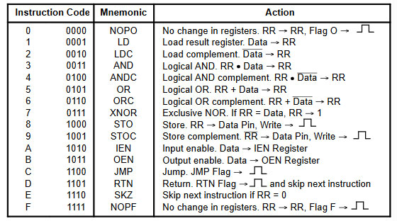


 In 1971 Intel created the first real microcessor chip the Intel 4004. It is a legendary chip amd not many are available nowadays.
 In 1972 Intel introduced their second real microcessor chip the Intel 8008. It is also a legendary chip amd not many are available nowadays.
 In 1974 the RCA 1802 (COSMAC 8-bit microprocessor family) became available, the processor design began in 1973. Most processors of that time were NMOS,
the 1802 was implemented in CMOS and used static logic. It did not have that much success for microcomputers and the company designed a (DIY) single board simple
computer called the COSMAC ELF, with switches to enter code and data and two hexadecimal LED displays. It was used as embedded controller especially aerospace and the
Hubble Space Telescope. The 1802 also ran the Galileo probe to Jupiter in 1989. Some computers were based on the 1802 like some ELF based systems, the
COMX-35 home computer and Telmac home computers in Finland only. The COMX-35 was the only computer that I knew and saw working. It is a funny but a little
strange processor.
In 1974 the RCA 1802 (COSMAC 8-bit microprocessor family) became available, the processor design began in 1973. Most processors of that time were NMOS,
the 1802 was implemented in CMOS and used static logic. It did not have that much success for microcomputers and the company designed a (DIY) single board simple
computer called the COSMAC ELF, with switches to enter code and data and two hexadecimal LED displays. It was used as embedded controller especially aerospace and the
Hubble Space Telescope. The 1802 also ran the Galileo probe to Jupiter in 1989. Some computers were based on the 1802 like some ELF based systems, the
COMX-35 home computer and Telmac home computers in Finland only. The COMX-35 was the only computer that I knew and saw working. It is a funny but a little
strange processor. In 1974, together with the MC6800 family Motorola introduced a PIA (Peripheral Interface Adapter) like the MC6820 as a 40 pin DIP chip to support the 6800
processor. It provided 20 I/O lines (two 8-bit bidirectional ports and 4 control lines for handshaking and interrupt generation. The MC6820 was used in the
Apple I to interface the ASCII keyboard and the display. It was also used in electronic pinball machines, the Atari 400 / Atari 800 and Commodore PET.
In 1974, together with the MC6800 family Motorola introduced a PIA (Peripheral Interface Adapter) like the MC6820 as a 40 pin DIP chip to support the 6800
processor. It provided 20 I/O lines (two 8-bit bidirectional ports and 4 control lines for handshaking and interrupt generation. The MC6820 was used in the
Apple I to interface the ASCII keyboard and the display. It was also used in electronic pinball machines, the Atari 400 / Atari 800 and Commodore PET.
 In 1974 Intel introduced the 8080 processor, and 8-bit microprocessor designed and manufactured by Intel and it was an extended and enhanced variant of the earlier
8008 design. The 8080 needs two support chips to function: the i8224 clock generator/driver and the i8228 bus controller. The first version was implemented in
NMOS and needed a +12 V and a −5 V and + 5 voltage. With its full 16-bit address bus it could access 64 KB of memory. It had a good competitor in the Z80, that
was binary compatible and had a lot of more instructions and registers. It was used in the Altair 8800 and S-100 bus personal computers and it was the base for
the CP/M operating system until the Z80 took over.
In 1974 Intel introduced the 8080 processor, and 8-bit microprocessor designed and manufactured by Intel and it was an extended and enhanced variant of the earlier
8008 design. The 8080 needs two support chips to function: the i8224 clock generator/driver and the i8228 bus controller. The first version was implemented in
NMOS and needed a +12 V and a −5 V and + 5 voltage. With its full 16-bit address bus it could access 64 KB of memory. It had a good competitor in the Z80, that
was binary compatible and had a lot of more instructions and registers. It was used in the Altair 8800 and S-100 bus personal computers and it was the base for
the CP/M operating system until the Z80 took over. In 1974 Intel produced some support chips for their 8080 processor and the 8224 chip was a single chip clock generator for the 8080 processor. It included circuits
to provide power-up reset, status strobe and sync of ready. It was mend to reduce the chip count of 8080 based computers.
In 1974 Intel produced some support chips for their 8080 processor and the 8224 chip was a single chip clock generator for the 8080 processor. It included circuits
to provide power-up reset, status strobe and sync of ready. It was mend to reduce the chip count of 8080 based computers. In 1974 Intel produced some support chips for their 8080 processor and the 8212 was an I/O chip designed for the Intel 8080/8085 processors. The device
comes in a 24-pin DIL package. Its main function is an 8-bit latch and an interrupt request flip-flop. It was mend to reduce the chip count of 8080 based
computers.
In 1974 Intel produced some support chips for their 8080 processor and the 8212 was an I/O chip designed for the Intel 8080/8085 processors. The device
comes in a 24-pin DIL package. Its main function is an 8-bit latch and an interrupt request flip-flop. It was mend to reduce the chip count of 8080 based
computers. In 1974 Motorola introduced the 6800 processor, it is an 8-bit microprocessor and one of the first that only needed a single 5V power supply. The 6800
has a 16-bit address bus that can directly access 64 KB of memory and an 8-bit bi-directional data bus. It has 72 instructions with seven addressing
modes for a total of 197 opcodes. The 6800 was popular in computer peripherals, test equipment applications and point-of-sale terminals. It also
found use in arcade games and pinball machines.
In 1974 Motorola introduced the 6800 processor, it is an 8-bit microprocessor and one of the first that only needed a single 5V power supply. The 6800
has a 16-bit address bus that can directly access 64 KB of memory and an 8-bit bi-directional data bus. It has 72 instructions with seven addressing
modes for a total of 197 opcodes. The 6800 was popular in computer peripherals, test equipment applications and point-of-sale terminals. It also
found use in arcade games and pinball machines.
 In 1975 MOS Technology introduced the 6502 8-bit microprocessor that was designed by a small team led by Chuck Peddle, a team that had formerly worked at Motorola
on the Motorola 6800 project. The 6502 is essentially a simplified, less expensive and faster version of the 6800 design. It was cheap and the biggest competitor
of the Z80 processor. I never used this processor, for me it was inferior to the Z80, with no I/O (only memory mapped I/O) and a very limited instruction set. But
the processor became very popular in systems like the Atari 2600, Atari 8-bit family, Apple II, Nintendo Entertainment System, Commodore 64, Atari Lynx, and the
BBC Microcomputer. Today the CMNOS version is still used in embedded systems. The difference between the 6502 and the 6502A is that the A version runs at 2 Mhz
and the normal 6502 version at 1Mhz.
I have two 40 pins DIL processors MOS6502 and UM6502A, but it is still not my favorite processor.
In 1975 MOS Technology introduced the 6502 8-bit microprocessor that was designed by a small team led by Chuck Peddle, a team that had formerly worked at Motorola
on the Motorola 6800 project. The 6502 is essentially a simplified, less expensive and faster version of the 6800 design. It was cheap and the biggest competitor
of the Z80 processor. I never used this processor, for me it was inferior to the Z80, with no I/O (only memory mapped I/O) and a very limited instruction set. But
the processor became very popular in systems like the Atari 2600, Atari 8-bit family, Apple II, Nintendo Entertainment System, Commodore 64, Atari Lynx, and the
BBC Microcomputer. Today the CMNOS version is still used in embedded systems. The difference between the 6502 and the 6502A is that the A version runs at 2 Mhz
and the normal 6502 version at 1Mhz.
I have two 40 pins DIL processors MOS6502 and UM6502A, but it is still not my favorite processor. In 1975 Rockwell introduced the R6532 (RIOT) Ram, I/O, Timer chip, that contained 128 x 8 bytes static ram, two 8 bit bidirectional data ports and a programmable timer
with interrupt capabilities. It was 6500 / 6800 bus compatible and I found the use of this chip in electronic pinball machines at that time and I know that the Atari 2600 used one.
In 1975 Rockwell introduced the R6532 (RIOT) Ram, I/O, Timer chip, that contained 128 x 8 bytes static ram, two 8 bit bidirectional data ports and a programmable timer
with interrupt capabilities. It was 6500 / 6800 bus compatible and I found the use of this chip in electronic pinball machines at that time and I know that the Atari 2600 used one.
 Am2900 is a family of integrated circuits (ICs) created in 1975 by Advanced Micro Devices (AMD). There is something special about this chip, the Am2900 family
was able to implement a CCU with data, addresses, and instructions to be any multiple of 4 bits by multiplying the number of ICs. The Am2901 chip was the
arithmetic-logic unit (ALU), and the “core” of the series. It could count using 4 bits and implement binary operations as well as various bit-shifting operations.
The 2901 and some other chips in the family were second sourced by an unusually large number of other manufacturers and was still in production in 2016.
Am2900 is a family of integrated circuits (ICs) created in 1975 by Advanced Micro Devices (AMD). There is something special about this chip, the Am2900 family
was able to implement a CCU with data, addresses, and instructions to be any multiple of 4 bits by multiplying the number of ICs. The Am2901 chip was the
arithmetic-logic unit (ALU), and the “core” of the series. It could count using 4 bits and implement binary operations as well as various bit-shifting operations.
The 2901 and some other chips in the family were second sourced by an unusually large number of other manufacturers and was still in production in 2016.
 The Signetics 2650 was introduced in July 1975 and it was an 8-bit microprocessor with a rather odd design. Because of the rather odd design and the
complex and odd memory access the processor was not used in commercial products that often. Actually the chip was designed in 1972 and the designer
selected the IBM 1130 as the model. But due to high chip production for Dolby the processor was only introduced in 1975. Advanced features were
status bits that were used to track the status of input/output devices and vectored interrupts. The 2650’s processor registers were divided into
two sets of three index registers, with a single global register R0 used as the accumulator. It had an odd address bus that was only 15 bits wide
and had some paging bits as well so only 8 KB could be addressed directly.
The Signetics 2650 was introduced in July 1975 and it was an 8-bit microprocessor with a rather odd design. Because of the rather odd design and the
complex and odd memory access the processor was not used in commercial products that often. Actually the chip was designed in 1972 and the designer
selected the IBM 1130 as the model. But due to high chip production for Dolby the processor was only introduced in 1975. Advanced features were
status bits that were used to track the status of input/output devices and vectored interrupts. The 2650’s processor registers were divided into
two sets of three index registers, with a single global register R0 used as the accumulator. It had an odd address bus that was only 15 bits wide
and had some paging bits as well so only 8 KB could be addressed directly.
 The Z80 (my first love as a processor) design started in 1974 when Federico Faggin left Intel to start the Zilog company with Ralph Ungermann. Faggin previously
worked as chief designer on, among others, the Intel 4004 and the 8080 processor. The Z80 is an 8 bit processor and officially released in 1976. The processor is
opcode compatible with Intel’s 8080 (which was a very slim move), but had more instructions, registers and addressing methods. The Z80 was designed for use in
computer terminals, printers, cash registers, but many home computers have also been produced based on the Z80 computer such as the TRS80, the Sinclair computer
series, the Philips P2000 and the well-known MSX computers. Even today there is still a club of avid hobbyists who build designs for the Z80 microprocessor.
The chip is still available. The Z80 processor was the main processor in my first TRS80 computer, the Sinclair ZX81, the Sinclair Spectrum, the MSX1 and MSX2
computer and the CP/M systems and embedded machine control units at my first job.
The Z80 (my first love as a processor) design started in 1974 when Federico Faggin left Intel to start the Zilog company with Ralph Ungermann. Faggin previously
worked as chief designer on, among others, the Intel 4004 and the 8080 processor. The Z80 is an 8 bit processor and officially released in 1976. The processor is
opcode compatible with Intel’s 8080 (which was a very slim move), but had more instructions, registers and addressing methods. The Z80 was designed for use in
computer terminals, printers, cash registers, but many home computers have also been produced based on the Z80 computer such as the TRS80, the Sinclair computer
series, the Philips P2000 and the well-known MSX computers. Even today there is still a club of avid hobbyists who build designs for the Z80 microprocessor.
The chip is still available. The Z80 processor was the main processor in my first TRS80 computer, the Sinclair ZX81, the Sinclair Spectrum, the MSX1 and MSX2
computer and the CP/M systems and embedded machine control units at my first job. This chip is basically just a digital parallel I/O port chip. You can configure the individual port pins as digital inputs or outputs and then use them for
whatever you want. The A/B input selects between either PortA or PortB and the C/D input selects between either the control register or the data register. The
control registers are used to configure the ports and the data registers are used to read/write the actual data. By connecting these to A0 and A1 one can access
the desired register using the address bus in an I/O read or write. The least significant bit of the memory address A0 then seledts the port A or B and the A1
line selects between the data and the control registers. With an address decoder you can put this chip anywhere in the I/O addressing space. In a lot of systems
this chip was used to add a parallel printer port to the Z80 system. But the chip can also handle digital inputs from switches and can be used to driver
signaling LEDs. One of the unique features of the Z80-PlO is that all data transfer between the peripheral device and the CPU can be accomplished
under total interrupt control even with nested interrupts. The the PlO can be programmed to interrupt if any specified peripheral alarm conditions
should occur. This interrupt capability reduces the amount of time that the processor has to spend in polling peripheral status.You can still buy
this chip and it costs only a few dollars.
This chip is basically just a digital parallel I/O port chip. You can configure the individual port pins as digital inputs or outputs and then use them for
whatever you want. The A/B input selects between either PortA or PortB and the C/D input selects between either the control register or the data register. The
control registers are used to configure the ports and the data registers are used to read/write the actual data. By connecting these to A0 and A1 one can access
the desired register using the address bus in an I/O read or write. The least significant bit of the memory address A0 then seledts the port A or B and the A1
line selects between the data and the control registers. With an address decoder you can put this chip anywhere in the I/O addressing space. In a lot of systems
this chip was used to add a parallel printer port to the Z80 system. But the chip can also handle digital inputs from switches and can be used to driver
signaling LEDs. One of the unique features of the Z80-PlO is that all data transfer between the peripheral device and the CPU can be accomplished
under total interrupt control even with nested interrupts. The the PlO can be programmed to interrupt if any specified peripheral alarm conditions
should occur. This interrupt capability reduces the amount of time that the processor has to spend in polling peripheral status.You can still buy
this chip and it costs only a few dollars. Together with the Z80 processor Zilog also produced some support chips and one of these chips was the Z80 SIO. It is basically a two channel serial input / output
device, with all control logic on board. Because a lot of Z80 systems were using a serial console for input and output, this was an important chip. It is a perfect
match with the Z80.
Together with the Z80 processor Zilog also produced some support chips and one of these chips was the Z80 SIO. It is basically a two channel serial input / output
device, with all control logic on board. Because a lot of Z80 systems were using a serial console for input and output, this was an important chip. It is a perfect
match with the Z80. Together with the Z80 processor Zilog also produced some support chips and one of these chips was the Z80 CTC. The Z80 CTC is a four-channel counter/timer that can be
programmed by system software for a broad range of counting and timing applications. These four independently programmable channels can be used for system event counting,
interrupt and interval timing, and clock rate generation.
Together with the Z80 processor Zilog also produced some support chips and one of these chips was the Z80 CTC. The Z80 CTC is a four-channel counter/timer that can be
programmed by system software for a broad range of counting and timing applications. These four independently programmable channels can be used for system event counting,
interrupt and interval timing, and clock rate generation. In 1976, National Semiconductor released the INS8060 or SC/MP (pronounced scamp) processor as a Simple Cost-effective Micro Processor. The processor had a few odd
quirks like a 12 bit program counter and four bank switch address bits on the data port and the odd ability to use one control pin to control three processors on
a single set of memory making it very easy to create a multiprocessor system. It also had to reduce costs a 1 bit ALU so the processor was not really fast. But
it was a nice simple design and the well-known electronics magazine Elektuur built several systems along. This was my first encounter with a microprocessor.
Sinclair released a board called MK14 with an SC/MP processor on it. In front of to the hobbyist it was a nice and relatively cheap processor, in the industry
it did not catch on. I bought one but at the last minute the buyer doubled the price, so I still do not have one.
In 1976, National Semiconductor released the INS8060 or SC/MP (pronounced scamp) processor as a Simple Cost-effective Micro Processor. The processor had a few odd
quirks like a 12 bit program counter and four bank switch address bits on the data port and the odd ability to use one control pin to control three processors on
a single set of memory making it very easy to create a multiprocessor system. It also had to reduce costs a 1 bit ALU so the processor was not really fast. But
it was a nice simple design and the well-known electronics magazine Elektuur built several systems along. This was my first encounter with a microprocessor.
Sinclair released a board called MK14 with an SC/MP processor on it. In front of to the hobbyist it was a nice and relatively cheap processor, in the industry
it did not catch on. I bought one but at the last minute the buyer doubled the price, so I still do not have one. In 1976 Intel introduced the 8085 8-bit microprocessor that was software-binary compatible with the Intel 8080 with only two minor instructions added. The 5 in
the part number was because the 8085 used only a single +5 V power supply, unlike the 8080 that required +5 V, −5 V and +12 V. The processor was a competitor
(Intel ‘s answer to) the very popular Z80 processor. The 8085 was often used as microcontroller in embedded systems thanks to its built-in serial I/O and
five prioritized interrupts, features that the Z80 CPU did not have. It was used in the famous VT102 terminal and the TRS-80 Model 100. The processor was
also cloned in the Soviet Union and also NASA used it in several space missions. I never used it, I was a Z80 fan.
In 1976 Intel introduced the 8085 8-bit microprocessor that was software-binary compatible with the Intel 8080 with only two minor instructions added. The 5 in
the part number was because the 8085 used only a single +5 V power supply, unlike the 8080 that required +5 V, −5 V and +12 V. The processor was a competitor
(Intel ‘s answer to) the very popular Z80 processor. The 8085 was often used as microcontroller in embedded systems thanks to its built-in serial I/O and
five prioritized interrupts, features that the Z80 CPU did not have. It was used in the famous VT102 terminal and the TRS-80 Model 100. The processor was
also cloned in the Soviet Union and also NASA used it in several space missions. I never used it, I was a Z80 fan.
 In 1976 Intel and NEC agreed that NEC could make second source chips from Intel and NEC also made and 8022 from Intel. The 8022 is as standard
MCS-48 series chip and has a modified Harvard architecture, with 2K × 8 ROM 64 × 8 RAM + A/D-converter. I cannot find any datasheet on this chip.
In 1976 Intel and NEC agreed that NEC could make second source chips from Intel and NEC also made and 8022 from Intel. The 8022 is as standard
MCS-48 series chip and has a modified Harvard architecture, with 2K × 8 ROM 64 × 8 RAM + A/D-converter. I cannot find any datasheet on this chip. In 1976 Intel introduced the MCS-48 microcontroller series, its first members were 8048, 8035 and 8748. In the beginning these chips were using NMOS
technology, later they became available in CMOS technology. The MCS-48 series has a modified Harvard architecture, with internal or external program
ROM and 64–256 bytes of internal (on-chip) RAM. The I/O is mapped into its own address space, separate from programs and data.The MCS-48 series was
later replaced by the very successful MCS-51 series but the chips are still used in cheap consumer electronics devices such as TV remotes, computer
keyboards. and toys. Compared to the standard 8048 the 8035 has no internal ROM and 64 x 8 bytes internal RAM memory.
In 1976 Intel introduced the MCS-48 microcontroller series, its first members were 8048, 8035 and 8748. In the beginning these chips were using NMOS
technology, later they became available in CMOS technology. The MCS-48 series has a modified Harvard architecture, with internal or external program
ROM and 64–256 bytes of internal (on-chip) RAM. The I/O is mapped into its own address space, separate from programs and data.The MCS-48 series was
later replaced by the very successful MCS-51 series but the chips are still used in cheap consumer electronics devices such as TV remotes, computer
keyboards. and toys. Compared to the standard 8048 the 8035 has no internal ROM and 64 x 8 bytes internal RAM memory.
 The 8039 is also a member of the MCS-48 processor family. Compared to the standard 8048 the 8039 equals to a 8035 and has no internal ROM and
128 x 8 bytes internal RAM memory on chip.
The 8039 is also a member of the MCS-48 processor family. Compared to the standard 8048 the 8039 equals to a 8035 and has no internal ROM and
128 x 8 bytes internal RAM memory on chip.
 The 8041 is also a member of the MCS-48 processor family and it use is a Universal Peripheral Interface 8 bit Slave Microcontroller. It has
1024 x 8 ROM and 64 x 8 RAM on chip. The 8041 is essentially a ‘‘slave’’ microcontroller, or a microcontroller with a slave interface included
on the chip. Interface registers are included to enable the UPI device to function as a slave peripheral controller in the MCS Modules and iAPX
family, as well as other 8-, 16-, and 32-bit systems.
The 8041 is also a member of the MCS-48 processor family and it use is a Universal Peripheral Interface 8 bit Slave Microcontroller. It has
1024 x 8 ROM and 64 x 8 RAM on chip. The 8041 is essentially a ‘‘slave’’ microcontroller, or a microcontroller with a slave interface included
on the chip. Interface registers are included to enable the UPI device to function as a slave peripheral controller in the MCS Modules and iAPX
family, as well as other 8-, 16-, and 32-bit systems.
 The 8741 is also a member of the MCS-48 processor family and it use is a Universal Peripheral Interface 8 bit Slave Microcontroller. It has
1024 x 8 EPROM and 64 x 8 RAM on chip. The 8741 is essentially a ‘‘slave’’ microcontroller, or a microcontroller with a slave interface included
on the chip. Interface registers are included to enable the UPI device to function as a slave peripheral controller in the MCS Modules and iAPX
family, as well as other 8-, 16-, and 32-bit systems.
I have four D8741 from NEC and two D8741 from Intel in my collection.
The 8741 is also a member of the MCS-48 processor family and it use is a Universal Peripheral Interface 8 bit Slave Microcontroller. It has
1024 x 8 EPROM and 64 x 8 RAM on chip. The 8741 is essentially a ‘‘slave’’ microcontroller, or a microcontroller with a slave interface included
on the chip. Interface registers are included to enable the UPI device to function as a slave peripheral controller in the MCS Modules and iAPX
family, as well as other 8-, 16-, and 32-bit systems.
I have four D8741 from NEC and two D8741 from Intel in my collection. The 8042 is also a member of the MCS-48 processor family and it use is a Universal Peripheral Interface 8 bit Slave Microcontroller. It has
4096 x 8 ROM and 256 x 8 RAM on chip. The 8042 is essentially a ‘‘slave’’ microcontroller, or a microcontroller with a slave interface included
on the chip. Interface registers are included to enable the UPI device to function as a slave peripheral controller in the MCS Modules and iAPX
family, as well as other 8-, 16-, and 32-bit systems.
The 8042 is also a member of the MCS-48 processor family and it use is a Universal Peripheral Interface 8 bit Slave Microcontroller. It has
4096 x 8 ROM and 256 x 8 RAM on chip. The 8042 is essentially a ‘‘slave’’ microcontroller, or a microcontroller with a slave interface included
on the chip. Interface registers are included to enable the UPI device to function as a slave peripheral controller in the MCS Modules and iAPX
family, as well as other 8-, 16-, and 32-bit systems.
 The 8748 is also a member of the MCS-48 processor family. Compared to the standard 8048 the 8748 has 1Kb x 8 bytes PROM and 64 x 8 bytes
internal RAM memory on chip, and 27 I/O lines.
The 8748 is also a member of the MCS-48 processor family. Compared to the standard 8048 the 8748 has 1Kb x 8 bytes PROM and 64 x 8 bytes
internal RAM memory on chip, and 27 I/O lines.
 The 8050 is also a member of the MCS-48 processor family. Compared to the standard 8048 the 8039 has 4K x 8 ROM and 256 × 8 RAM memory on chip.
 In 1974, together with the MC6800 family Motorola introduced a PIA (Peripheral Interface Adapter) like the MC6820 as a 40 pin DIP chip to support
the 6800 processor. It provided 20 I/O lines (two 8-bit bidirectional ports and 4 control lines for handshaking and interrupt generation. In 1976 Motorola
switched the MC6800 family to a depletion-mode technology so the MC6820 became the MC6821. The MC6820 was used in the Apple I to interface the ASCII keyboard
and the display. The Tandy Color Computer used two MC6821s to provide I/O access to the video, audio and peripherals.
In 1974, together with the MC6800 family Motorola introduced a PIA (Peripheral Interface Adapter) like the MC6820 as a 40 pin DIP chip to support
the 6800 processor. It provided 20 I/O lines (two 8-bit bidirectional ports and 4 control lines for handshaking and interrupt generation. In 1976 Motorola
switched the MC6800 family to a depletion-mode technology so the MC6820 became the MC6821. The MC6820 was used in the Apple I to interface the ASCII keyboard
and the display. The Tandy Color Computer used two MC6821s to provide I/O access to the video, audio and peripherals.
 In June 1976 Texas Instruments introduced the TMS9900 processor and it was one of the first commercially available, single-chip 16-bit microprocessors. It
implemented Texas Instruments’ TI-990 minicomputer architecture in a single-chip but the 64-pin DIP format made it more expensive to implement in smaller
machines than the more common 40-pin DIP chips. It was used in the Texas Instruments own home computer the TI-99/4. It has a little strange architecture
compared to other microprocessors of that time, given its origin from a mini-computer.
In June 1976 Texas Instruments introduced the TMS9900 processor and it was one of the first commercially available, single-chip 16-bit microprocessors. It
implemented Texas Instruments’ TI-990 minicomputer architecture in a single-chip but the 64-pin DIP format made it more expensive to implement in smaller
machines than the more common 40-pin DIP chips. It was used in the Texas Instruments own home computer the TI-99/4. It has a little strange architecture
compared to other microprocessors of that time, given its origin from a mini-computer. In 1976 (as far as I know) Intel introduced the P8274 Multi Protocol Serial Controller. It had two independent full duplex transmitters and receivers,
it could do asynchronous, Byte synchronous and Bit synchronous operation and was fully compatible with the 8048, 8051, 8085, 8088, 8086 CPU’s.
It supported 4 independent DMA channels.
In 1976 (as far as I know) Intel introduced the P8274 Multi Protocol Serial Controller. It had two independent full duplex transmitters and receivers,
it could do asynchronous, Byte synchronous and Bit synchronous operation and was fully compatible with the 8048, 8051, 8085, 8088, 8086 CPU’s.
It supported 4 independent DMA channels.
 In 1976 AMD introduced the P8253 Programmeble Interval Timer chipas as a licensed Intel second source. The P8253 is a programmable interval timer/counter
specially designed for Intel processors that can be treated as a series of I/O ports for access.
In 1976 AMD introduced the P8253 Programmeble Interval Timer chipas as a licensed Intel second source. The P8253 is a programmable interval timer/counter
specially designed for Intel processors that can be treated as a series of I/O ports for access.
 The Intel 3242 is an address multiplexer and refresh counter for multiplexed address dynamic rams. The chip a 7-bit refresh counter that is
externally controlled so it can support distributed and burst refresh. It is often used together with 2116 dram chips.
The Intel 3242 is an address multiplexer and refresh counter for multiplexed address dynamic rams. The chip a 7-bit refresh counter that is
externally controlled so it can support distributed and burst refresh. It is often used together with 2116 dram chips.
 In 1977 AMD reverse engineered the Intel 8080 processor and created the Am9080 a chip that could replace the 8080 chip. It was
originally produced without license but later an agreement was made with Intel to become a licensed second source for the 8080.
It is not a very common chip to find.
In 1977 AMD reverse engineered the Intel 8080 processor and created the Am9080 a chip that could replace the 8080 chip. It was
originally produced without license but later an agreement was made with Intel to become a licensed second source for the 8080.
It is not a very common chip to find.
 In 1977 Motorola introduced the 6802 processor based on the already famous 6800 design. It was a 8-bit microprocessor and it had a 16-bit address bus that
could directly access 64 KB of memory. The 6800 processor has 72 instructions with seven addressing modes for a total of 197 opcodes. The MC6802 included
128 bytes of RAM and an internal clock oscillator on chip.
In 1977 Motorola introduced the 6802 processor based on the already famous 6800 design. It was a 8-bit microprocessor and it had a 16-bit address bus that
could directly access 64 KB of memory. The 6800 processor has 72 instructions with seven addressing modes for a total of 197 opcodes. The MC6802 included
128 bytes of RAM and an internal clock oscillator on chip.
 In 1977 Motorola introduced the MC14500B (ICU) to replace relay systems and programmable logic controllers and serial data manipulation. The processor supports
16 commands and is operating at a frequency of 1 MHz. It does not have a program counter (PC), instead, a clock signal drives a separate chip that also determines
the supported memory size. The ICU architecture seems to be similar to that of the DEC PDP-14 computer.
In 1977 Motorola introduced the MC14500B (ICU) to replace relay systems and programmable logic controllers and serial data manipulation. The processor supports
16 commands and is operating at a frequency of 1 MHz. It does not have a program counter (PC), instead, a clock signal drives a separate chip that also determines
the supported memory size. The ICU architecture seems to be similar to that of the DEC PDP-14 computer. In 1977 Motorola introduced the MC6845 Display controller and it was widely used in 8-bit computers during the 1980s. It was originally designed for
the Motorola 6800 CPU but used for many more processors like the Zilog Z80 and MOS 6502. It was not a one in all solution, it needed other chips to
function and the implementation of that hardware is entirely up to the designer. It was used in the BBC Micro, Amstrad CPC, and Videx VideoTerm display
cards for the Apple II. It was also used in early graphics adapter cards for the IBM PC like the MDA, Hercules Graphics Card and Color Graphics Adapter (CGA).
In 1977 Motorola introduced the MC6845 Display controller and it was widely used in 8-bit computers during the 1980s. It was originally designed for
the Motorola 6800 CPU but used for many more processors like the Zilog Z80 and MOS 6502. It was not a one in all solution, it needed other chips to
function and the implementation of that hardware is entirely up to the designer. It was used in the BBC Micro, Amstrad CPC, and Videx VideoTerm display
cards for the Apple II. It was also used in early graphics adapter cards for the IBM PC like the MDA, Hercules Graphics Card and Color Graphics Adapter (CGA). In 1977 MOS Technology introduced the 6522 Versatile Interface Adapter (VIA), as an I/O port controller for the 6502 family of microprocessors. It provided two
bidirectional 8-bit parallel I/O ports, two 16-bit timers and an 8-bit shift register for serial communications. The 6522 was widely used in computers of the
1980s, particularly Commodore’s machines, the Apple III, Oric-1 and Oric Atmos, BBC Micro, Victor 9000 / Sirius 1, the Apple Macintosh and the Vectrex game console.
In 1977 MOS Technology introduced the 6522 Versatile Interface Adapter (VIA), as an I/O port controller for the 6502 family of microprocessors. It provided two
bidirectional 8-bit parallel I/O ports, two 16-bit timers and an 8-bit shift register for serial communications. The 6522 was widely used in computers of the
1980s, particularly Commodore’s machines, the Apple III, Oric-1 and Oric Atmos, BBC Micro, Victor 9000 / Sirius 1, the Apple Macintosh and the Vectrex game console.
 In 1977 Intel introduced the P8155 as support chip for the 8085 (and 8088) processor. It contains 2038 bits (256 x 8 bytes) static Ram, two programmeble 8 bit I/O
ports and one 6 bit programmeble I/O port and a 14 bit programmeble timer / counter. It was an attempt of Intel to lower the chip count in 8085 and 8088 designs.
In 1977 Intel introduced the P8155 as support chip for the 8085 (and 8088) processor. It contains 2038 bits (256 x 8 bytes) static Ram, two programmeble 8 bit I/O
ports and one 6 bit programmeble I/O port and a 14 bit programmeble timer / counter. It was an attempt of Intel to lower the chip count in 8085 and 8088 designs. The Intel 8243 contains four 4-bit I/O ports which serve as an extension to the on-chip I/O and are addressed as port 4 to 7. This chip is specially
designed for the 8048 processor and supports transfer from accumulator to port, port to accumulator, AND accumulator to port and OR accumulator to port.
The Intel 8243 contains four 4-bit I/O ports which serve as an extension to the on-chip I/O and are addressed as port 4 to 7. This chip is specially
designed for the 8048 processor and supports transfer from accumulator to port, port to accumulator, AND accumulator to port and OR accumulator to port. The MK3870 is an 8-bit microcontroller and a single chip implementation of Fairchild F8. The microcontroller includes up to 4 KB mask-programmable ROM, 64 bytes
scratchpad RAM and up to 64 bytes executable RAM. The MCU also integrates 32-bit I/O and programmable timer. There was also a MK38P70 development version of
the 3870 MCU that supported external EPROM chip. It was used in the Heathkit Aircraft Navigation Computer OCW-1401 that was basically a special calculator.
The MK3870 is an 8-bit microcontroller and a single chip implementation of Fairchild F8. The microcontroller includes up to 4 KB mask-programmable ROM, 64 bytes
scratchpad RAM and up to 64 bytes executable RAM. The MCU also integrates 32-bit I/O and programmable timer. There was also a MK38P70 development version of
the 3870 MCU that supported external EPROM chip. It was used in the Heathkit Aircraft Navigation Computer OCW-1401 that was basically a special calculator. In 1978 Motorola introduced the 6809, an 8-bit microprocessor with some 16-bit features. It was source compatible with Motorola 6800 but offered some good improvements.
Compared to other popular processors of that time it was very expensive (4 times the price of a Z80). It was used in the TRS-80 Color Computer, Dragon 32/64, SuperPET,
the famous Vectrex game console, and some arcade machines. I have never programmed this processor, but it is nice to have one.
In 1978 Motorola introduced the 6809, an 8-bit microprocessor with some 16-bit features. It was source compatible with Motorola 6800 but offered some good improvements.
Compared to other popular processors of that time it was very expensive (4 times the price of a Z80). It was used in the TRS-80 Color Computer, Dragon 32/64, SuperPET,
the famous Vectrex game console, and some arcade machines. I have never programmed this processor, but it is nice to have one. In 1978 Motorola also introduced the 6803, an 8-bit microprocessor with some 16-bit features. It was source compatible with Motorola 6800 but offered some good
improvements like the 6801 and 6802. The MC6803 had no ROM and fewer different bus configurations. I have never programmed this processor, but it is nice to have one.
In 1978 Motorola also introduced the 6803, an 8-bit microprocessor with some 16-bit features. It was source compatible with Motorola 6800 but offered some good
improvements like the 6801 and 6802. The MC6803 had no ROM and fewer different bus configurations. I have never programmed this processor, but it is nice to have one. In 1978 Motorola also introduced the 6840, the MC6840 programmable counter had three 16-bit binary counters that could be used for frequency measurement,
event counting, or interval measurement.
In 1978 Motorola also introduced the 6840, the MC6840 programmable counter had three 16-bit binary counters that could be used for frequency measurement,
event counting, or interval measurement. In 1978 Intel released the 8086 processor, the 8086 was also called iAPX 86 and it is a 16-bit microprocessor. The 8086 was the base
of all x86 architecture that became Intel’s most successful line of processors. I used this processor a lot and the segment registers that Intel used
in the 8086 CPU’s to access one megabyte of memory was a “pain in the ass” for many programmers. I used to replace the Intel processors
by the NEC version.
In 1978 Intel released the 8086 processor, the 8086 was also called iAPX 86 and it is a 16-bit microprocessor. The 8086 was the base
of all x86 architecture that became Intel’s most successful line of processors. I used this processor a lot and the segment registers that Intel used
in the 8086 CPU’s to access one megabyte of memory was a “pain in the ass” for many programmers. I used to replace the Intel processors
by the NEC version. In 1978 Intel also introduced the 8087 Floating-point Co-Processor, it is the math coprocessor for the Intel 8086 series of microprocessors. The popularity
of the 8087 got a real boost when IBM included a coprocessor socket on the IBM PC motherboard. The development of the 8087 led to the IEEE 754-1985 standard
for floating-point arithmetic.
In 1978 Intel also introduced the 8087 Floating-point Co-Processor, it is the math coprocessor for the Intel 8086 series of microprocessors. The popularity
of the 8087 got a real boost when IBM included a coprocessor socket on the IBM PC motherboard. The development of the 8087 led to the IEEE 754-1985 standard
for floating-point arithmetic.  In 1978 by General Instrument introduced the AY-3-8910 sound chip. It is a 3-voice programmable sound generator (PSG). The AY-3-8910 and its variants were
used in many arcade games and pinball machines but it was also the typical sound chip in the Intellivision and Vectrex video game consoles, the Amstrad CPC,
Oric-1, Colour Genie, MSX, and later ZX Spectrum home computers. It was also used in the Mockingboard and Cricket sound cards for the Apple II and the
Speech / Sound Cartridge for the TRS-80 Color Computer. After General Instrument’s spinoff of Microchip Technology in 1987, the chip was sold for a few years
under the Microchip brand. It was also manufactured under license by Yamaha as the YM2149F, the Atari ST uses this version.
In 1978 by General Instrument introduced the AY-3-8910 sound chip. It is a 3-voice programmable sound generator (PSG). The AY-3-8910 and its variants were
used in many arcade games and pinball machines but it was also the typical sound chip in the Intellivision and Vectrex video game consoles, the Amstrad CPC,
Oric-1, Colour Genie, MSX, and later ZX Spectrum home computers. It was also used in the Mockingboard and Cricket sound cards for the Apple II and the
Speech / Sound Cartridge for the TRS-80 Color Computer. After General Instrument’s spinoff of Microchip Technology in 1987, the chip was sold for a few years
under the Microchip brand. It was also manufactured under license by Yamaha as the YM2149F, the Atari ST uses this version.  In 1978 Texas Instruments introduced the SN76477 complex sound generator. The chip is typically used as a sound effects generator in arcade games
and toys. The use of the SN76477 in a musical context is limited by the fact that it was difficult to electronically control the pitch of the
produced sound. The SN76477 generates complex audio combining the outputs of a LFO, VCO and noise generator, through an envelope ADSR. The sound
generation is controlled by supplying control voltages, logic levels and different resistor and capacitor values.
In 1978 Texas Instruments introduced the SN76477 complex sound generator. The chip is typically used as a sound effects generator in arcade games
and toys. The use of the SN76477 in a musical context is limited by the fact that it was difficult to electronically control the pitch of the
produced sound. The SN76477 generates complex audio combining the outputs of a LFO, VCO and noise generator, through an envelope ADSR. The sound
generation is controlled by supplying control voltages, logic levels and different resistor and capacitor values. In 1979 Motorola introduced the 68000 processor, a 16/32-bit complex instruction set computer (CISC) microprocessor. It has a 32-bit instruction set, 32-bit registers
and a 16-bit internal data bus, the address bus is 24 bits and it uses a 16-bit ALU. The processor was used in a few high end computers like the Macintosh, Amiga and
Atari ST, and the Mega Drive console. All of these were known because of their great graphic capabilities. These system were too expensive for me at the time and so
I have never programmed a 68000 processor, but I have one MC68000P12 processor. Nowadays the 68000 architecture is still in use.
In 1979 Motorola introduced the 68000 processor, a 16/32-bit complex instruction set computer (CISC) microprocessor. It has a 32-bit instruction set, 32-bit registers
and a 16-bit internal data bus, the address bus is 24 bits and it uses a 16-bit ALU. The processor was used in a few high end computers like the Macintosh, Amiga and
Atari ST, and the Mega Drive console. All of these were known because of their great graphic capabilities. These system were too expensive for me at the time and so
I have never programmed a 68000 processor, but I have one MC68000P12 processor. Nowadays the 68000 architecture is still in use. Intel introduced the Intel 8088 on June 1, 1979, the processor has an eight-bit external data bus instead of the 16-bit bus of the 8086. The 16-bit registers
and the one megabyte address range are unchanged, it was intended to be a version of the 8086 for cheaper system. The original IBM PC used the 8088 at a clock
frequency of 4.77 MHz. Some of IBM’s engineers wanted another (better) processor but Intel offered the best price. This processor was the beginning of the whole
x86 processor range of Intel.
Intel introduced the Intel 8088 on June 1, 1979, the processor has an eight-bit external data bus instead of the 16-bit bus of the 8086. The 16-bit registers
and the one megabyte address range are unchanged, it was intended to be a version of the 8086 for cheaper system. The original IBM PC used the 8088 at a clock
frequency of 4.77 MHz. Some of IBM’s engineers wanted another (better) processor but Intel offered the best price. This processor was the beginning of the whole
x86 processor range of Intel. In 1979 Texas Instruments introduced the TMS9918 video display controller (VDC). This is a famous video processor that was used in a lot of systems like the
ColecoVision, CreatiVision, Memotech MTX, MSX, SG-1000/SC-3000, Spectravideo, Sord M5, Sega game gear, Texas Instruments TI-99/4 and the Casio PV-2000. The TMS9918
generates both grid-based character graphics (used to display text or background images) and sprites used for moving foreground objects. I have used this
processor and programmed it in my first MSX-1 computer. The TMS9928 and TMS9929 are variants of the TMS9918.
In 1979 Texas Instruments introduced the TMS9918 video display controller (VDC). This is a famous video processor that was used in a lot of systems like the
ColecoVision, CreatiVision, Memotech MTX, MSX, SG-1000/SC-3000, Spectravideo, Sord M5, Sega game gear, Texas Instruments TI-99/4 and the Casio PV-2000. The TMS9918
generates both grid-based character graphics (used to display text or background images) and sprites used for moving foreground objects. I have used this
processor and programmed it in my first MSX-1 computer. The TMS9928 and TMS9929 are variants of the TMS9918.  In 1979 Texas Instruments also introduced the TMS9118 video display controller (VDC). This is a lesser used famous video processor that was used in some MSX-1 computers.
The TMS9118 is a variant of the TMS9918 with a different external ram configuration of 16K x 4 ram chips.
In 1979 Texas Instruments also introduced the TMS9118 video display controller (VDC). This is a lesser used famous video processor that was used in some MSX-1 computers.
The TMS9118 is a variant of the TMS9918 with a different external ram configuration of 16K x 4 ram chips.
 In 1979 Motorola introduced the MC6847P video display controller (VDC). It was used in the TRS-80 Color Computer, Dragon 32/64, Laser 200, TRS-80 MC-10,
NEC PC-6000 series, Acorn Atom, and it is a relatively simple display generator compared to other display chips of the time. It is capable of displaying
text and graphics contained within a roughly square display matrix 256 pixels wide by 192 lines high. The ROM includes a 5 x 7 pixel font, compatible
with 6-bit ASCII. Effects such as inverse video or colored text are possible. It is capable of displaying nine colors. The low display resolution was
a necessity of using television sets as display monitors.
In 1979 Motorola introduced the MC6847P video display controller (VDC). It was used in the TRS-80 Color Computer, Dragon 32/64, Laser 200, TRS-80 MC-10,
NEC PC-6000 series, Acorn Atom, and it is a relatively simple display generator compared to other display chips of the time. It is capable of displaying
text and graphics contained within a roughly square display matrix 256 pixels wide by 192 lines high. The ROM includes a 5 x 7 pixel font, compatible
with 6-bit ASCII. Effects such as inverse video or colored text are possible. It is capable of displaying nine colors. The low display resolution was
a necessity of using television sets as display monitors.  In 1979 Mullard introduced the SAA5050, a character generator chip for implementing the Teletext character set. The SAA5050 was used in teletext-equipped
television sets, viewdata terminals, and microcomputers like the Philips P2000, Acorn System 2 and BBC Microcomputer. The chip generated appropriate
video output for a 7-bit input character code representing the current character on the text line, full-screen resolution generated by the SAA5050
was 480×500 pixels, corresponding to 40×25 characters.
In 1979 Mullard introduced the SAA5050, a character generator chip for implementing the Teletext character set. The SAA5050 was used in teletext-equipped
television sets, viewdata terminals, and microcomputers like the Philips P2000, Acorn System 2 and BBC Microcomputer. The chip generated appropriate
video output for a 7-bit input character code representing the current character on the text line, full-screen resolution generated by the SAA5050
was 480×500 pixels, corresponding to 40×25 characters. The SAA5051 is also a character generator chip for implementing the Teletext character set, with a German characterset. The SAA5051 was used in teletext-equipped
television sets, viewdata terminals, and microcomputers. The chip generated appropriate video output for a 7-bit input character code representing the current
character on the text line, full-screen resolution generated by the SAA5051 was 480×500 pixels, corresponding to 40×25 characters.
The SAA5051 is also a character generator chip for implementing the Teletext character set, with a German characterset. The SAA5051 was used in teletext-equipped
television sets, viewdata terminals, and microcomputers. The chip generated appropriate video output for a 7-bit input character code representing the current
character on the text line, full-screen resolution generated by the SAA5051 was 480×500 pixels, corresponding to 40×25 characters.
 In 1979 Zilog introduced the Z8 microcontroller architecture. One of the features is up to 4,096 fast on-chip registers which may be used as accumulators, pointers
or as ordinary random-access memory (RAM). A 16-bit address space for between 1 kB and 64 kB of either PROM, ROM or flash memory and there is even a second 16-bit
address space. On chip peripherals include analog-to-digital converter, Serial Peripheral Interface (SPI) bus and I²C channels, IrDA encoders / decoders etc.
There are versions with from 8 up to 80 pins and a lot of different packages.
In 1979 Zilog introduced the Z8 microcontroller architecture. One of the features is up to 4,096 fast on-chip registers which may be used as accumulators, pointers
or as ordinary random-access memory (RAM). A 16-bit address space for between 1 kB and 64 kB of either PROM, ROM or flash memory and there is even a second 16-bit
address space. On chip peripherals include analog-to-digital converter, Serial Peripheral Interface (SPI) bus and I²C channels, IrDA encoders / decoders etc.
There are versions with from 8 up to 80 pins and a lot of different packages. This chip is an Intel Multifunction microprocessor support controller with a SIO (Serial interface) and PIO (Parallel interface), timers and an Interrupt controller
all in one chip. I do not know the year it cam out and I never used one but I have calculated it came ouit around 1979.
This chip is an Intel Multifunction microprocessor support controller with a SIO (Serial interface) and PIO (Parallel interface), timers and an Interrupt controller
all in one chip. I do not know the year it cam out and I never used one but I have calculated it came ouit around 1979.  This chip is a PIO ( parallel Input Output) device from NEC with 24 programmable I/O lines. It can be used in the same way as an Z80 PIO. I do not know
the year it cam out and I never used one but I have calculated it came ouit around 1979. NEC produced all Intel chips as second source under licence since 1976.
This chip is a PIO ( parallel Input Output) device from NEC with 24 programmable I/O lines. It can be used in the same way as an Z80 PIO. I do not know
the year it cam out and I never used one but I have calculated it came ouit around 1979. NEC produced all Intel chips as second source under licence since 1976.
 The 8259 is a Programmable Interrupt Controller (PIC) designed for the Intel 8085 and Intel 8086 microprocessors. The 8259 combines multiple interrupt input sources
to a single interrupt output to the host microprocessor, expanding the interrupt levels available in a system.
The 8259A was the interrupt controller for the ISA bus in the IBM PC and IBM PC AT and IBM also used the NEC chips for this.
NEC produced all Intel chips as second source under licence since 1976.
The 8259 is a Programmable Interrupt Controller (PIC) designed for the Intel 8085 and Intel 8086 microprocessors. The 8259 combines multiple interrupt input sources
to a single interrupt output to the host microprocessor, expanding the interrupt levels available in a system.
The 8259A was the interrupt controller for the ISA bus in the IBM PC and IBM PC AT and IBM also used the NEC chips for this.
NEC produced all Intel chips as second source under licence since 1976.
 The uPD765AC from NEC is a an LSI floppy disk controller (FDC) chip which contains the circuitry and control functions for interfacing a processor to 4 floppy
disk drives. . It is capableof either IBM 3740 singledensity format (FM), or IBM System 34 double density format (MFM) including double-sided recording.
The uPD765AC from NEC is a an LSI floppy disk controller (FDC) chip which contains the circuitry and control functions for interfacing a processor to 4 floppy
disk drives. . It is capableof either IBM 3740 singledensity format (FM), or IBM System 34 double density format (MFM) including double-sided recording.
 The UPB8214 from NEC is an eight-level priority interrupt controller, designed to simplify interrupt driven microcomputer systems. The interrupt structure
of the microcomputer system can be expanded beyond eight interrupt levels by cascading UPB8214s.
The UPB8214 from NEC is an eight-level priority interrupt controller, designed to simplify interrupt driven microcomputer systems. The interrupt structure
of the microcomputer system can be expanded beyond eight interrupt levels by cascading UPB8214s.
 The INS8243 is a n I/O expander specially designed for the INS8048 / INS8049 and INS8050 processors. It consists of five, four bit bidirectional
I/O ports in a 24 DIP package.
The INS8243 is a n I/O expander specially designed for the INS8048 / INS8049 and INS8050 processors. It consists of five, four bit bidirectional
I/O ports in a 24 DIP package.  The Intel 8251 is a standard Universal Synchronous/Asynchronous Receiver/Transmitter (USART) designed for the MCS-48, 8080, 8085, 8086 and 8088 processors.
NEC produced all Intel chips as second source under licence.
The Intel 8251 is a standard Universal Synchronous/Asynchronous Receiver/Transmitter (USART) designed for the MCS-48, 8080, 8085, 8086 and 8088 processors.
NEC produced all Intel chips as second source under licence.
 The AM2964 from AMD is a Dynamic Memory Controller (DMC), it has two 8 bit latches to hold the memory addresses. It also has a refresh counter to update
the refresh of the 16K or 64K dynamic rams.
The AM2964 from AMD is a Dynamic Memory Controller (DMC), it has two 8 bit latches to hold the memory addresses. It also has a refresh counter to update
the refresh of the 16K or 64K dynamic rams.
 The Intel 8089 is a microprocessor dedicated for inpu/outpu processing. It is made for the 8088 and 8086 processors and the chip performs
the function of an inteliogent DMA controller for the Intel iAPX 86 family. It can operate completely parallel with the CPU giving dramaticly
improved I/O performance. The chip has two I/O channels supporting a transferrate up to 1.25 mbyte/sec. It is not a very common chip.
The Intel 8089 is a microprocessor dedicated for inpu/outpu processing. It is made for the 8088 and 8086 processors and the chip performs
the function of an inteliogent DMA controller for the Intel iAPX 86 family. It can operate completely parallel with the CPU giving dramaticly
improved I/O performance. The chip has two I/O channels supporting a transferrate up to 1.25 mbyte/sec. It is not a very common chip. In 1980 Intel released the 8031 (family of the 8051) microcontroller and I have have used this one in my first modem design with and external eprom. The 8031 is just like
the 8051 an eight bit CISC processor. The 8031 had no rom and only 128 bytes ram on board which was a big challenge for the programmer. By default, the processor had a
number of Timers multiple interrupt lines and an internal serial uart on board and many programmable I/O pins. The processor wasn’t expensive and was used as a central
processor in many devices. Even today this processor is still used and it still is available.
I have several types of this processor like original Intel P8031, a SAB8031 (Siemens) and P80C321 (AMD)
In 1980 Intel released the 8031 (family of the 8051) microcontroller and I have have used this one in my first modem design with and external eprom. The 8031 is just like
the 8051 an eight bit CISC processor. The 8031 had no rom and only 128 bytes ram on board which was a big challenge for the programmer. By default, the processor had a
number of Timers multiple interrupt lines and an internal serial uart on board and many programmable I/O pins. The processor wasn’t expensive and was used as a central
processor in many devices. Even today this processor is still used and it still is available.
I have several types of this processor like original Intel P8031, a SAB8031 (Siemens) and P80C321 (AMD) In 1980 Intel released the 8051 microcontroller and I have designed many circuits and devices (modems) with this processor myself. The 8051 is an eight bit CISC processor
that has been marketed in many types, also by many other manufacturers of which Atmel is the is best known. The system normally had 4 kb rom and 256 bytes ram on board
which was a big challenge for the programmer. But there could also 64 kb of ROM and 64 kb of RAM can be connected externally, sacrificing many I/O pins. By default, the
processor had a number of Timers multiple interrupt lines and an internal serial uart on board and many programmable I/O pins. The processor wasn’t expensive either
and was used as a central processor in many devices. Even today this processor is still used and it still is available.
In 1980 Intel released the 8051 microcontroller and I have designed many circuits and devices (modems) with this processor myself. The 8051 is an eight bit CISC processor
that has been marketed in many types, also by many other manufacturers of which Atmel is the is best known. The system normally had 4 kb rom and 256 bytes ram on board
which was a big challenge for the programmer. But there could also 64 kb of ROM and 64 kb of RAM can be connected externally, sacrificing many I/O pins. By default, the
processor had a number of Timers multiple interrupt lines and an internal serial uart on board and many programmable I/O pins. The processor wasn’t expensive either
and was used as a central processor in many devices. Even today this processor is still used and it still is available. In 1980 Intel released the P8344AH, another variant of the 8051 microcontroller The 8051 is an eight bit CISC processor
that has been marketed in many types, also by many other manufacturers of which Atmel is the is best known. This chip has 4 kb rom and 192 bytes ram on board
which is a big challenge for the programmer. But there could also 64 kb of ROM and 64 kb of RAM can be connected externally, sacrificing many I/O pins. By default, the
processor had a number of Timers multiple interrupt lines and an internal serial uart on board and many programmable I/O pins. The processor wasn’t expensive either
and was used as a central processor in many devices.
In 1980 Intel released the P8344AH, another variant of the 8051 microcontroller The 8051 is an eight bit CISC processor
that has been marketed in many types, also by many other manufacturers of which Atmel is the is best known. This chip has 4 kb rom and 192 bytes ram on board
which is a big challenge for the programmer. But there could also 64 kb of ROM and 64 kb of RAM can be connected externally, sacrificing many I/O pins. By default, the
processor had a number of Timers multiple interrupt lines and an internal serial uart on board and many programmable I/O pins. The processor wasn’t expensive either
and was used as a central processor in many devices. The Intel P8044 is the same as the P8344, but has on chip 4Kb factory masked rom on board.
 The Intel C8744 is the same as the P8344, but has on chip 4Kb Programmable/UV Erasable EPROM on board and with on-chip serial
communication controller for SDLC/HDLC.
The Intel C8744 is the same as the P8344, but has on chip 4Kb Programmable/UV Erasable EPROM on board and with on-chip serial
communication controller for SDLC/HDLC. The 8051 is the basic bare 8-bit CPU from Intel, it has 8-bit registers (one 16-bit register with special move instructions),
8-bit data bus and 2×16-bit address buses, program counter, data pointer. Four fast switchable register banks with eight registers memory mapped),
fast interrupt with optional register bank switching and selectable priority, 128 bytes of on-chip RAM (IRAM), three full) 8-bit bi-directional
input/output ports, bit addressable UART (serial port) and two 16-bit counter/timers. It is indeed a MCU chip.
The 8051 is the basic bare 8-bit CPU from Intel, it has 8-bit registers (one 16-bit register with special move instructions),
8-bit data bus and 2×16-bit address buses, program counter, data pointer. Four fast switchable register banks with eight registers memory mapped),
fast interrupt with optional register bank switching and selectable priority, 128 bytes of on-chip RAM (IRAM), three full) 8-bit bi-directional
input/output ports, bit addressable UART (serial port) and two 16-bit counter/timers. It is indeed a MCU chip. The 8052 is the basic bare 8-bit CPU from Intel, it has 8-bit registers (one 16-bit register with special move instructions),
8-bit data bus and 2×16-bit address buses, program counter, data pointer. Four fast switchable register banks with eight registers memory mapped),
fast interrupt with optional register bank switching and selectable priority, three full) 8-bit bi-directional
input/output ports, bit addressable UART (serial port) and three 16-bit counter/timers. It is indeed a MCU chip. The 8052 was an enhanced version
of the original 8051 that features 256 bytes of internal RAM instead of 128 bytes, 8 KB of ROM instead of 4 KB, and a third 16-bit timer. Most
modern 8051-compatible microcontrollers include these features.
The 8052 is the basic bare 8-bit CPU from Intel, it has 8-bit registers (one 16-bit register with special move instructions),
8-bit data bus and 2×16-bit address buses, program counter, data pointer. Four fast switchable register banks with eight registers memory mapped),
fast interrupt with optional register bank switching and selectable priority, three full) 8-bit bi-directional
input/output ports, bit addressable UART (serial port) and three 16-bit counter/timers. It is indeed a MCU chip. The 8052 was an enhanced version
of the original 8051 that features 256 bytes of internal RAM instead of 128 bytes, 8 KB of ROM instead of 4 KB, and a third 16-bit timer. Most
modern 8051-compatible microcontrollers include these features. The 8751 is an EPROM version of the 8051AH. It has 4 Kbytes of electrically programmable ROM which can be erased with ultraviolet light.
It is fully compatible with the 8051AH but incorporates s Program Memory Security bit that can be used to protect the EPROM against readout
The 8751 is an EPROM version of the 8051AH. It has 4 Kbytes of electrically programmable ROM which can be erased with ultraviolet light.
It is fully compatible with the 8051AH but incorporates s Program Memory Security bit that can be used to protect the EPROM against readout In 1980 introduceerde Texas Intruments de SN76489 sound chip. It is a complex sound generator and has 3 programmeble tone generators,
a programmable white noise generator and programmeble attenuation.The SN76489 was originally designed to be used in the TI-99/4 computer,
where it was first called the TMS9919 and later SN94624, when it was sold outside of TI it was renamed to the SN76489.
Sega used this chip in the Sega Master System, Game Gear, and Sega Genesis game consoles.
In 1980 introduceerde Texas Intruments de SN76489 sound chip. It is a complex sound generator and has 3 programmeble tone generators,
a programmable white noise generator and programmeble attenuation.The SN76489 was originally designed to be used in the TI-99/4 computer,
where it was first called the TMS9919 and later SN94624, when it was sold outside of TI it was renamed to the SN76489.
Sega used this chip in the Sega Master System, Game Gear, and Sega Genesis game consoles.  In 1980 Intel introduced the P80C152, an Universal Communications Controller based on the 8051 8-Bit microcontroller architecture. It had a
8K Factory Mask Programmable ROM and was intended as a Multi-Protocol Serial Communication controller for SDLC / HDLC, CSMA / CD and SDLC / HDLC
or User Definable Protocols, Full Duplex / Half Duplex extra I/O ports and much more. I have one because it is a 8051 based device.
In 1980 Intel introduced the P80C152, an Universal Communications Controller based on the 8051 8-Bit microcontroller architecture. It had a
8K Factory Mask Programmable ROM and was intended as a Multi-Protocol Serial Communication controller for SDLC / HDLC, CSMA / CD and SDLC / HDLC
or User Definable Protocols, Full Duplex / Half Duplex extra I/O ports and much more. I have one because it is a 8051 based device.
 In 1980 Intel introduced the 8237, a direct memory access (DMA) controller a part of the MCS 85 microprocessor family. It enables data transfer
between memory and the I/O with reduced load on the system’s main processor. The 8237 is a four-channel device that can be expanded to include
any number of DMA channel inputs. A single 8237 was used as the DMA controller in the original IBM PC and IBM XT. The IBM PC AT added another
8237 in master-slave configuration, increasing the number of DMA channels from four to seven.
In 1980 Intel introduced the 8237, a direct memory access (DMA) controller a part of the MCS 85 microprocessor family. It enables data transfer
between memory and the I/O with reduced load on the system’s main processor. The 8237 is a four-channel device that can be expanded to include
any number of DMA channel inputs. A single 8237 was used as the DMA controller in the original IBM PC and IBM XT. The IBM PC AT added another
8237 in master-slave configuration, increasing the number of DMA channels from four to seven.
 In 1980 Commodore brought the VIC-20 computer on the market and it had a MOS6561(VIC video chip) on board. The history of this chip goes back to 1977
and it was Mos and Commodore that made the final version. Its features include: 16 kB address space for screen, character and color memory, 16 colors
two selectable character sizes, video resolution (176 × 184) VIC-20, although up to 256 × 280 is possible on PAL, 4 channel sound system (3 square wave
+ “white” noise + global volume setting), on-chip DMA, two 8-bit analog-to-digital converters, light pen support. Programmable characters are the only
way of creating graphics and animation on the VIC as the chip does not have sprites or an all-points-addressable bitmap mode.
In 1980 Commodore brought the VIC-20 computer on the market and it had a MOS6561(VIC video chip) on board. The history of this chip goes back to 1977
and it was Mos and Commodore that made the final version. Its features include: 16 kB address space for screen, character and color memory, 16 colors
two selectable character sizes, video resolution (176 × 184) VIC-20, although up to 256 × 280 is possible on PAL, 4 channel sound system (3 square wave
+ “white” noise + global volume setting), on-chip DMA, two 8-bit analog-to-digital converters, light pen support. Programmable characters are the only
way of creating graphics and animation on the VIC as the chip does not have sprites or an all-points-addressable bitmap mode.
 The 80A is an 8-bit microprocessor that was manufactured by VEB Mikroelektronik in the German DDR. Production started in 1980 and the 80A is an unlicensed
clone of the Zilog Z80 microprocessor, also supporting illegal opcodes and bugs.
The 80A is an 8-bit microprocessor that was manufactured by VEB Mikroelektronik in the German DDR. Production started in 1980 and the 80A is an unlicensed
clone of the Zilog Z80 microprocessor, also supporting illegal opcodes and bugs.
 The Intel 8293 is a bidirectional transceiver and it was designed to interface the Intel 8291A GPIB Talker/Listener and the 8293 GPIB controller
for IEEE 488-1978 standard instrumentation. It can also be used as a standard three-state open collector bus transceiver.
The Intel 8293 is a bidirectional transceiver and it was designed to interface the Intel 8291A GPIB Talker/Listener and the 8293 GPIB controller
for IEEE 488-1978 standard instrumentation. It can also be used as a standard three-state open collector bus transceiver.
 In 1981 National Instruments introduced the TMS9914 a General Purpose Interface Bus Adapter. It is designed to implement all of the functions
define in the IEEE 488-1975 standard. It was one of the support chips of the TMS9900 processor, I do not know that much about this chip,
or where it was used.
In 1981 National Instruments introduced the TMS9914 a General Purpose Interface Bus Adapter. It is designed to implement all of the functions
define in the IEEE 488-1975 standard. It was one of the support chips of the TMS9900 processor, I do not know that much about this chip,
or where it was used.
 I do not know the exact introduction date but calculating it should be around 1981 when NEC started to make Intel compatible chips. This chip is
a clock generator and driver for the Intel 8086 and 8088 processor and a replacement for the Intel 8284 chip. As I also collect variant of chips
I got one of these too, it is a small 18 pins chip.
I do not know the exact introduction date but calculating it should be around 1981 when NEC started to make Intel compatible chips. This chip is
a clock generator and driver for the Intel 8086 and 8088 processor and a replacement for the Intel 8284 chip. As I also collect variant of chips
I got one of these too, it is a small 18 pins chip.
 The WD8250 from Western Digital is a programmable Asynchronous communication element (ACE) and it is used as a serial I/O device and can be used
in either polling of interrupt mode. It can be interfaced to most common microprocessors like the Z80, 8080, 8088 and 6800 and supports full double buffering.
The WD8250 from Western Digital is a programmable Asynchronous communication element (ACE) and it is used as a serial I/O device and can be used
in either polling of interrupt mode. It can be interfaced to most common microprocessors like the Z80, 8080, 8088 and 6800 and supports full double buffering.
 In 1982 NEC also put a 8086 variant on the market, these processors were compatible with the original Intel 8086 processor from 1978. The 8086 was also called
iAPX 86 and it is a 16-bit microprocessor the 8086 was the base of all the x86 architecture that became Intel’s most successful line of processors. I have
used this processor a lot and the four 16-bit segment registers that allowed the 8086 CPU to access one megabyte of memory was a “pain in the ass” for a
lot of programmers. I used to replace the Intel processors with the NEC versions.
In 1982 NEC also put a 8086 variant on the market, these processors were compatible with the original Intel 8086 processor from 1978. The 8086 was also called
iAPX 86 and it is a 16-bit microprocessor the 8086 was the base of all the x86 architecture that became Intel’s most successful line of processors. I have
used this processor a lot and the four 16-bit segment registers that allowed the 8086 CPU to access one megabyte of memory was a “pain in the ass” for a
lot of programmers. I used to replace the Intel processors with the NEC versions.  In 1982 Motorola released the 68008 as an 8/32-bit microprocessor, it is a version of the standard Motorola 68000 with an 8-bit external data bus, as well as a
smaller address bus. The 68008 was available with 20 or 22 address lines (respective to 48-pin or 52-pin package) which allowed 1 MB or 4 MB address space versus
the 16 MB addressable on the 68000. The 68008 processor was designed to work with lower cost and simpler 8-bit memory systems, but this mad it also half as fast
as an standard 68000 processor, but still much faster than the 8-bit competitors.
In 1982 Motorola released the 68008 as an 8/32-bit microprocessor, it is a version of the standard Motorola 68000 with an 8-bit external data bus, as well as a
smaller address bus. The 68008 was available with 20 or 22 address lines (respective to 48-pin or 52-pin package) which allowed 1 MB or 4 MB address space versus
the 16 MB addressable on the 68000. The 68008 processor was designed to work with lower cost and simpler 8-bit memory systems, but this mad it also half as fast
as an standard 68000 processor, but still much faster than the 8-bit competitors.
 In 1982 Motorola released the MC68010 processor as the successor to the Motorola 68000. This processor fixes several small flaws in the 68000, and adds a
few features. The 68010 is pin-compatible with the 68000, but is not 100% software compatible. In practice, the overall speed gain to a 68000 processor at
the same frequency is less than 10% and the 68010 was never as popular as the 68000.
In 1982 Motorola released the MC68010 processor as the successor to the Motorola 68000. This processor fixes several small flaws in the 68000, and adds a
few features. The 68010 is pin-compatible with the 68000, but is not 100% software compatible. In practice, the overall speed gain to a 68000 processor at
the same frequency is less than 10% and the 68010 was never as popular as the 68000.
 In 1982 Intel introduced the 80186 processor (also known as the iAPX 186) it was based on the Intel 8086 and had a 16-bit external data bus multiplexed with a 20-bit
address bus. The 80188 variant, with an 8-bit external data bus was also available. The 80186 series was generally intended for embedded systems. The Original
IBM-PC was not hardware compatible with the 80186 to it changed the hardware to a IBM PC/AT. The processor was used in a lot of other PC’s too and I did a
lot of assembly / C programming for this processor.
In 1982 Intel introduced the 80186 processor (also known as the iAPX 186) it was based on the Intel 8086 and had a 16-bit external data bus multiplexed with a 20-bit
address bus. The 80188 variant, with an 8-bit external data bus was also available. The 80186 series was generally intended for embedded systems. The Original
IBM-PC was not hardware compatible with the 80186 to it changed the hardware to a IBM PC/AT. The processor was used in a lot of other PC’s too and I did a
lot of assembly / C programming for this processor. In 1982 Intel also introduced the 80286 processor (also known as the iAPX 286) iut was based on the 8086 and 80186 CPU’s with separate, non-multiplexed address and
data buses and also the first with memory management and wide protection abilities. A good feature was that it was backward code compatible with the earlier
Intel 8086 and 8088 processors. The 80286 was used in the IBM PC/AT, introduced in 1984 and then widely used in most PC/AT compatible computers. I did a lot
of assembly / C programming for this processor.
In 1982 Intel also introduced the 80286 processor (also known as the iAPX 286) iut was based on the 8086 and 80186 CPU’s with separate, non-multiplexed address and
data buses and also the first with memory management and wide protection abilities. A good feature was that it was backward code compatible with the earlier
Intel 8086 and 8088 processors. The 80286 was used in the IBM PC/AT, introduced in 1984 and then widely used in most PC/AT compatible computers. I did a lot
of assembly / C programming for this processor. In 1982 Intel also introduced the 80287 Floating-point Co-Processor, it is the math coprocessor for the Intel 80286 series of microprocessors. The x87 provides single-precision,
double-precision and 80-bit double-extended precision binary floating-point arithmetic as per the IEEE 754-1985 standard. By default, the x87 processors all
use 80-bit double-extended precision internally.
In 1982 Intel also introduced the 80287 Floating-point Co-Processor, it is the math coprocessor for the Intel 80286 series of microprocessors. The x87 provides single-precision,
double-precision and 80-bit double-extended precision binary floating-point arithmetic as per the IEEE 754-1985 standard. By default, the x87 processors all
use 80-bit double-extended precision internally. In 1982 Texas Instruments introduced the TMS9937 single chip video/controller, a 40 pin chip that could generate video timing signals for
standard and non-standard CRT monitors, both interlaced and non-interlaced. I don’t have that much information about this chip besides the datasheet.
In 1982 Texas Instruments introduced the TMS9937 single chip video/controller, a 40 pin chip that could generate video timing signals for
standard and non-standard CRT monitors, both interlaced and non-interlaced. I don’t have that much information about this chip besides the datasheet.
 I do not know exactly when this processor came out, but it was special produced for the Commodore 64 so I connected this processor to the date of the C64. The
MOS Technology 6510 is an 8-bit microprocessor and it is a slightly modified form of the very successful 6502. The primary change from the 6502 was the addition
of an 8-bit general purpose I/O port and the address bus could be made tristate.
I do not know exactly when this processor came out, but it was special produced for the Commodore 64 so I connected this processor to the date of the C64. The
MOS Technology 6510 is an 8-bit microprocessor and it is a slightly modified form of the very successful 6502. The primary change from the 6502 was the addition
of an 8-bit general purpose I/O port and the address bus could be made tristate.  In 1983 NEC introduced the uPD71059 Interrupt Control Unit as a low power CMOS programmable interrupt controller for microcomputer system
and it can process eight interrupt requests allocating a priority level to each one. It transfers the interrupt with the highest priority
to the processor with interrupt address information. By cascading 8 slave it can process 64 interrupts.
In 1983 NEC introduced the uPD71059 Interrupt Control Unit as a low power CMOS programmable interrupt controller for microcomputer system
and it can process eight interrupt requests allocating a priority level to each one. It transfers the interrupt with the highest priority
to the processor with interrupt address information. By cascading 8 slave it can process 64 interrupts. In 1982 Intel was very active in the Ethernet standardization and implementation and they introduced a Ethernet controller chip for their 80186 and 80188
processors. I do not know the exact date of the chip, but when I read the history of Ethernet and Intel it should be around this year. It is a big chip
with 48 pins. It supported networks up to 10 Mb/s.
In 1982 Intel was very active in the Ethernet standardization and implementation and they introduced a Ethernet controller chip for their 80186 and 80188
processors. I do not know the exact date of the chip, but when I read the history of Ethernet and Intel it should be around this year. It is a big chip
with 48 pins. It supported networks up to 10 Mb/s. The AM29x305 is based on the Signetics N8X305, that’s was an improved version of the SMS300, a non-traditional design processor
that focused on manipulation of signals. It had 16-bit instructions, but operated on data 8 bits at a time. It had very limited
ways of accessing external memory was designed as perhaps the first DSP. AMD second sourced this processor.
The AM29x305 is based on the Signetics N8X305, that’s was an improved version of the SMS300, a non-traditional design processor
that focused on manipulation of signals. It had 16-bit instructions, but operated on data 8 bits at a time. It had very limited
ways of accessing external memory was designed as perhaps the first DSP. AMD second sourced this processor. In 1983 Yamaha produced the YM2149, a clone of the famous AY-3-8910 (see above) under license from General Instrument. This chip was also used in many home computers
as replacement of the AY-3-8910. The Yamaha YM2149 shares the same pinout as the AY-3-8910 with the minor difference that pin number 26 could halve the master
clock if pulled down. If not connected, as it would replace an AY-3-8910.
In 1983 Yamaha produced the YM2149, a clone of the famous AY-3-8910 (see above) under license from General Instrument. This chip was also used in many home computers
as replacement of the AY-3-8910. The Yamaha YM2149 shares the same pinout as the AY-3-8910 with the minor difference that pin number 26 could halve the master
clock if pulled down. If not connected, as it would replace an AY-3-8910. In 1983 Motola introduced the MC68230 (Parallel Interface/Timer) chip, a 64 dip chip in line with the big chips Motorola used to
make. It was a double buffered I/O chip for the MC68000 series processors, the I/O ports could be 8 or 16 bits wide and the
timer could be used for interrupts, wave generation, time measurements and watchdog timer.
In 1983 Motola introduced the MC68230 (Parallel Interface/Timer) chip, a 64 dip chip in line with the big chips Motorola used to
make. It was a double buffered I/O chip for the MC68000 series processors, the I/O ports could be 8 or 16 bits wide and the
timer could be used for interrupts, wave generation, time measurements and watchdog timer. In 1983 the EM83050H microcontroller was dedicated to be a keyboard encoder specially designed for IBM PC XT/AT and all compatible
machines. The EM83050H controls all scan codes, three LEDs status, scan timing and communications between the keyboard and PC. It
is easy to implement a high performance, low cost keyboard with the minimal external components.
In 1983 the EM83050H microcontroller was dedicated to be a keyboard encoder specially designed for IBM PC XT/AT and all compatible
machines. The EM83050H controls all scan codes, three LEDs status, scan timing and communications between the keyboard and PC. It
is easy to implement a high performance, low cost keyboard with the minimal external components. In 1983 the Commodore 64 came on the market and it used the MOS906114-01 PLA chip. The PLA is used to make chip selection signals
to determine which chip should be connected to the data bus. Therefore, the PLA is responsible for dictating the memory map of the C64 and
enables the implementation of bank switching. Commodore engineer James Redfield said it was the “glue logic of connecting everything together”.
The chip was very sensitive and most defective on the Commodore 64, until a better version was released.
In 1983 the Commodore 64 came on the market and it used the MOS906114-01 PLA chip. The PLA is used to make chip selection signals
to determine which chip should be connected to the data bus. Therefore, the PLA is responsible for dictating the memory map of the C64 and
enables the implementation of bank switching. Commodore engineer James Redfield said it was the “glue logic of connecting everything together”.
The chip was very sensitive and most defective on the Commodore 64, until a better version was released. Nintendo created a custom version of the 6502 processor for their Famicon and NES consoles, also for a reason to protect them from clones of their console.
When the demand of consoles got very high they also got these chips from UMC in Taiwan. After a while UMC offered NES clone chips as a standard commercial
product and as Taiwan did not agree to any copyright agreement (worldwide) and they do not respect intellectual property, Nintendo had no recourse against
UMC. These chips are still available.
Nintendo created a custom version of the 6502 processor for their Famicon and NES consoles, also for a reason to protect them from clones of their console.
When the demand of consoles got very high they also got these chips from UMC in Taiwan. After a while UMC offered NES clone chips as a standard commercial
product and as Taiwan did not agree to any copyright agreement (worldwide) and they do not respect intellectual property, Nintendo had no recourse against
UMC. These chips are still available. The AM8228 is a single chip System Controller Databus driver for the AM9080A Microcomputer system and the 8080A compatible processor. It generates
alle control signals for memory and I/O. Interrupt processing is done by means of a single vectored interrupt.
The AM8228 is a single chip System Controller Databus driver for the AM9080A Microcomputer system and the 8080A compatible processor. It generates
alle control signals for memory and I/O. Interrupt processing is done by means of a single vectored interrupt. The Atmel AT89C2051 Processor was based on the Intel 8051 architecture but in a 20 pin dip case. I do not know when it first came out but I know that Atmel was
founded in 1984. The AT89C2051 provides the following standard features: 2K bytes of Flash, 128 bytes of RAM, 15 I/O lines, two 16-bit timer/counters, a five
vector two-level interrupt architecture, a full duplex serial port, a precision analog comparator, on-chip oscillator and clock circuitry. It is used in several
digital clock designs. Even today this processor is still used and it still is available, but atmel was taken over by Microchip, so now most of these
chais are also available with the prefix STC. The AT89C2051 has 2K bytes of Flash, 128 bytes of RAM, the AT89S52 has 8K bytes of Flash, 256 bytes of RAM,
the AT89S8253 has 12K bytes of Flash, 256 bytes of RAM, the AT89C55 has 20K bytes of Flash, 256 bytes of RAM.
I have one AT89C2051 also a AT89S52, STC89C52RC and a AT89S8253 and a AT89C55 processor.
The Atmel AT89C2051 Processor was based on the Intel 8051 architecture but in a 20 pin dip case. I do not know when it first came out but I know that Atmel was
founded in 1984. The AT89C2051 provides the following standard features: 2K bytes of Flash, 128 bytes of RAM, 15 I/O lines, two 16-bit timer/counters, a five
vector two-level interrupt architecture, a full duplex serial port, a precision analog comparator, on-chip oscillator and clock circuitry. It is used in several
digital clock designs. Even today this processor is still used and it still is available, but atmel was taken over by Microchip, so now most of these
chais are also available with the prefix STC. The AT89C2051 has 2K bytes of Flash, 128 bytes of RAM, the AT89S52 has 8K bytes of Flash, 256 bytes of RAM,
the AT89S8253 has 12K bytes of Flash, 256 bytes of RAM, the AT89C55 has 20K bytes of Flash, 256 bytes of RAM.
I have one AT89C2051 also a AT89S52, STC89C52RC and a AT89S8253 and a AT89C55 processor. In 1984 NEC created the V20 as pin compatible with the Intel 8088 but much faster, I switched my 8088 processor in my PC to a V20 to gain some performance. The V20 was
also offered a mode that emulated an Intel 8080. Late 1984 Intel filed suit against NEC, claiming that the microcode in the V20 and V30 infringed its patents for the 8088
and 8086 processors. (See V30).
In 1984 NEC created the V20 as pin compatible with the Intel 8088 but much faster, I switched my 8088 processor in my PC to a V20 to gain some performance. The V20 was
also offered a mode that emulated an Intel 8080. Late 1984 Intel filed suit against NEC, claiming that the microcode in the V20 and V30 infringed its patents for the 8088
and 8086 processors. (See V30). In 1984 NEC created the V30 as pin compatible with the Intel 8086 but much faster, I switched my 8086 processor in my PC to a V30 to gain some performance. The V30 was
also used in the Psion Series 3, the NEC PC-9801VM, the Olivetti PCS86 and in various arcade machines. Late 1984 Intel filed suit against NEC, claiming that the microcode
in the V20 and V30 infringed its patents for the 8088 and 8086 processors. In its ruling, the court determined that the microcode in the control store constitutes a
computer program, and so is protected by copyright but also determined that NEC did not simply copy Intel’s microcode, and that the microcode in the V20 and V30 was
sufficiently different from Intel’s to not infringe Intel’s patents. I still have one processor because of the wonderful history and this processors lawsuit established
the legality of reverse engineering.
In 1984 NEC created the V30 as pin compatible with the Intel 8086 but much faster, I switched my 8086 processor in my PC to a V30 to gain some performance. The V30 was
also used in the Psion Series 3, the NEC PC-9801VM, the Olivetti PCS86 and in various arcade machines. Late 1984 Intel filed suit against NEC, claiming that the microcode
in the V20 and V30 infringed its patents for the 8088 and 8086 processors. In its ruling, the court determined that the microcode in the control store constitutes a
computer program, and so is protected by copyright but also determined that NEC did not simply copy Intel’s microcode, and that the microcode in the V20 and V30 was
sufficiently different from Intel’s to not infringe Intel’s patents. I still have one processor because of the wonderful history and this processors lawsuit established
the legality of reverse engineering.  In 1984 Motorola introduced the 68HC11 8-bit microcontroller (µC) family, now produced by NXP Semiconductors. The 68HC11 is based on the Motorola 6800 microprocessor
and are used in automotive applications, barcode readers, hotel card key writers, robotics and various embedded systems. The MC68HC11A8 was the first microcontroller
to include CMOS EEPROM. The HC11 instruction set is backward compatible with the 6800 but has an extra Y index register and 16 Bits instructions and register combinations.
In 1984 Motorola introduced the 68HC11 8-bit microcontroller (µC) family, now produced by NXP Semiconductors. The 68HC11 is based on the Motorola 6800 microprocessor
and are used in automotive applications, barcode readers, hotel card key writers, robotics and various embedded systems. The MC68HC11A8 was the first microcontroller
to include CMOS EEPROM. The HC11 instruction set is backward compatible with the 6800 but has an extra Y index register and 16 Bits instructions and register combinations.
 In 1984 Yamaha introduced the YM2203, also known as OPN a sound chip based on FM Operator technology. Is has a six channel (3 FM and 3 SSG)
sound channels and this chip was used in all kinds of videogame and computer systems throughout the 1980s and early 1990s. Internally it was
a variation of the Yamaha’s YM2149F SSG chip.
In 1984 Yamaha introduced the YM2203, also known as OPN a sound chip based on FM Operator technology. Is has a six channel (3 FM and 3 SSG)
sound channels and this chip was used in all kinds of videogame and computer systems throughout the 1980s and early 1990s. Internally it was
a variation of the Yamaha’s YM2149F SSG chip. In 1984 the Oric Atmos compouter was released and it used a semi-custom ASIC (ULA) for the video display that also manages the interface between
the processor The two modes are a low resolution text mode, with a user defined characterset with 28 rows of 40 characters and a high resolution mode
with 200 rows of 240 pixels above three lines of text. In Bulgaria the Atmos was cloned named Pravetz 8D and I got my chip from Bulgaria.
In 1984 the Oric Atmos compouter was released and it used a semi-custom ASIC (ULA) for the video display that also manages the interface between
the processor The two modes are a low resolution text mode, with a user defined characterset with 28 rows of 40 characters and a high resolution mode
with 200 rows of 240 pixels above three lines of text. In Bulgaria the Atmos was cloned named Pravetz 8D and I got my chip from Bulgaria.
 In de Commodore 16 (1884) zat een TED chip, a video chip that also contained sound generation hardware, DRAM refresh circuitry, interval timers,
and keyboard input handling. It was designed for the Commodore Plus/4 and 16 and the packaging is 48-pin DIP. The video capabilities provided by
the TED were largely a subset of those in the VIC-II. The TED featured a simple tone generator that produced two channels of audio, the first channel
produced a square wave and the second could produce either a square wave or white noise. I do not have a datasheet only a reference to a wikipeadia page.
In de Commodore 16 (1884) zat een TED chip, a video chip that also contained sound generation hardware, DRAM refresh circuitry, interval timers,
and keyboard input handling. It was designed for the Commodore Plus/4 and 16 and the packaging is 48-pin DIP. The video capabilities provided by
the TED were largely a subset of those in the VIC-II. The TED featured a simple tone generator that produced two channels of audio, the first channel
produced a square wave and the second could produce either a square wave or white noise. I do not have a datasheet only a reference to a wikipeadia page.
 The MC2681 is a dual universal asynchonous receiver/transmitter (DUART) and it is a part of the MC6800 Family of peripherals and interfaces to the
MC68000 processor via a general purpous interface. The device also has a multypurpose 7-bit input port and a multypurpose 8-bit output port that can be
used as generel input/output ports but also can be assigned specific functions like clock inputs or status / interrupt outputs.
The MC2681 is a dual universal asynchonous receiver/transmitter (DUART) and it is a part of the MC6800 Family of peripherals and interfaces to the
MC68000 processor via a general purpous interface. The device also has a multypurpose 7-bit input port and a multypurpose 8-bit output port that can be
used as generel input/output ports but also can be assigned specific functions like clock inputs or status / interrupt outputs.
 The MC68HC05C4 of Motorola is low-cost single-chip microcomputers. This 8-bit microcomputer contains an on-chip oscillator, 176 Bytes of On-Chip RAM,
4160 Bytes of On-Chip ROM, 24 Bidirectional 1/0 Lines, 16-Bit Timer, two Serial Communications Interfaces, it is similar to MC6800 and has Versatile
Interrupt Handling. It is a rathe small chip and the pins are very close together.
The MC68HC05C4 of Motorola is low-cost single-chip microcomputers. This 8-bit microcomputer contains an on-chip oscillator, 176 Bytes of On-Chip RAM,
4160 Bytes of On-Chip ROM, 24 Bidirectional 1/0 Lines, 16-Bit Timer, two Serial Communications Interfaces, it is similar to MC6800 and has Versatile
Interrupt Handling. It is a rathe small chip and the pins are very close together.
 In 1984 Hitachi introduced the HD63484 ACRTC Advanced CRT Controller chip an improvement of the NEC µ7220, that was already a powerful graphics
controller. It could support a resolution up to 4096 × 4096 in a 1-bit mode within a 2 Mbyte display memory and was very popular and used in a lot
of terminals and PC graphics boards. When IBM introduced their EGA, this became the standard for mainstream PCs but anyone that wanted high-resolution,
bit-mapped graphics there was the Hitachi HD63484.
In 1984 Hitachi introduced the HD63484 ACRTC Advanced CRT Controller chip an improvement of the NEC µ7220, that was already a powerful graphics
controller. It could support a resolution up to 4096 × 4096 in a 1-bit mode within a 2 Mbyte display memory and was very popular and used in a lot
of terminals and PC graphics boards. When IBM introduced their EGA, this became the standard for mainstream PCs but anyone that wanted high-resolution,
bit-mapped graphics there was the Hitachi HD63484.
 The UPB8282 (and UPB8283) are 8 bit latches with three-state output buffers. The 8282 is non-inverting and the 8283 inverts the inputs. These
chips were used to demultiplex the address / data lines on 8042, 8080, 8085 and 8086 processors.
The UPB8282 (and UPB8283) are 8 bit latches with three-state output buffers. The 8282 is non-inverting and the 8283 inverts the inputs. These
chips were used to demultiplex the address / data lines on 8042, 8080, 8085 and 8086 processors.
 In 1984 Freescal introduced the MC68701 microcontroller unit (MCU) a single chip microcomputer that was an enhanced version of the 6800 processor
and source and object code compatible with the Motorola 6800. It has and enhanced 6800 instructionset, 8 x 8 multiply instructiuon, serial
interface, 16 bit timer, 64 K addressing space, bus compatible with 6800, 2048 bytes of UV erasable Eprom and 128 bytes of internal ram,
29 I/O lines and internal clock generator.
In 1984 Freescal introduced the MC68701 microcontroller unit (MCU) a single chip microcomputer that was an enhanced version of the 6800 processor
and source and object code compatible with the Motorola 6800. It has and enhanced 6800 instructionset, 8 x 8 multiply instructiuon, serial
interface, 16 bit timer, 64 K addressing space, bus compatible with 6800, 2048 bytes of UV erasable Eprom and 128 bytes of internal ram,
29 I/O lines and internal clock generator.
 The Mitsubishi M50955 is based on the Mitsubishi 740, also known as MELPS 740. This was a series of 8-bit CMOS microcontrollers with an
enhanced MOS Technology 6502 compatible core was primarily intended for single-chip implementations, and included optional RAM and ROM or
EPROM on-chip. Other additions included a variety of optional timers, input/output lines, and many other features. The M50955 was the
parts with internal Mask-ROM.
The Mitsubishi M50955 is based on the Mitsubishi 740, also known as MELPS 740. This was a series of 8-bit CMOS microcontrollers with an
enhanced MOS Technology 6502 compatible core was primarily intended for single-chip implementations, and included optional RAM and ROM or
EPROM on-chip. Other additions included a variety of optional timers, input/output lines, and many other features. The M50955 was the
parts with internal Mask-ROM. In 1985 Hitachi introduced the HD614023S based on the Hitachi HMCS40 family of 4-bit microcontrollers developed and introduced in the late 1970s. Two types of each chip
were manufactured, one using pMOS for low cost and another using CMOS where lower power was more desired. Hitachi later also introduce a replacement series called the
HMCS400. The chips contained 4-bit ALU performing BCD arithmetic. 512 to 2,048 Words of program ROM. Additional 128 Words of pattern ROM. 32 to 160 digits of data
RAM. Chips also contained Event/Timer-Counter and 22-44 I/O lines. Output was aimed for driving dot matrix Liquid Crystal displays. The HMCS40 was used in a very
large array of games, toys, controllers, and office equipment.
In 1985 Hitachi introduced the HD614023S based on the Hitachi HMCS40 family of 4-bit microcontrollers developed and introduced in the late 1970s. Two types of each chip
were manufactured, one using pMOS for low cost and another using CMOS where lower power was more desired. Hitachi later also introduce a replacement series called the
HMCS400. The chips contained 4-bit ALU performing BCD arithmetic. 512 to 2,048 Words of program ROM. Additional 128 Words of pattern ROM. 32 to 160 digits of data
RAM. Chips also contained Event/Timer-Counter and 22-44 I/O lines. Output was aimed for driving dot matrix Liquid Crystal displays. The HMCS40 was used in a very
large array of games, toys, controllers, and office equipment.  In 1885 Yamaha introduced the YM3812, it was the first in the OPL family, providing a nine channel, two operator synthesizer. It was used in a Commodore 64 expansion,
the Sound Expander, as well as several arcade games, such as Terra Cresta and Bubble Bobble. A very closely related chip is the Y8950 or MSX-AUDIO, which was used
as an MSX expansion unit. It is in basic a YM3526 with ADPCM recording and playback capability.
In 1885 Yamaha introduced the YM3812, it was the first in the OPL family, providing a nine channel, two operator synthesizer. It was used in a Commodore 64 expansion,
the Sound Expander, as well as several arcade games, such as Terra Cresta and Bubble Bobble. A very closely related chip is the Y8950 or MSX-AUDIO, which was used
as an MSX expansion unit. It is in basic a YM3526 with ADPCM recording and playback capability.  In 1885 Motorola introduced the MC68HC681 DUAL ASYNCHRONOUS RECEIVER/TRANSMITTER DUART) to the M68000 Family of peripherals
and directly interfaces to the MC68000 processor via an asynchronous bus structure. The MC68HC681 consists of these major sections:
Internal Control Logic, Timing Logic, Interrupt Control Logic, Bidirectional 8-bit Data Bus Buffer, Two Independent Communication
Channels (A and B), 6-bit Parallel Input Port, 8-bit Parallel Output Port.
In 1885 Motorola introduced the MC68HC681 DUAL ASYNCHRONOUS RECEIVER/TRANSMITTER DUART) to the M68000 Family of peripherals
and directly interfaces to the MC68000 processor via an asynchronous bus structure. The MC68HC681 consists of these major sections:
Internal Control Logic, Timing Logic, Interrupt Control Logic, Bidirectional 8-bit Data Bus Buffer, Two Independent Communication
Channels (A and B), 6-bit Parallel Input Port, 8-bit Parallel Output Port.
 In 1986 AMD (Advanced Micro Devices) introduced the AM33C93A and enhanced SCSI bus interface controller. It was compatible with a lot
of microprocessors trough and 8 bit bus. Small Computer System Interface (SCSI) is a set of standards for physically connecting and
transferring data between computers and peripheral devices such as disk drives.
In 1986 AMD (Advanced Micro Devices) introduced the AM33C93A and enhanced SCSI bus interface controller. It was compatible with a lot
of microprocessors trough and 8 bit bus. Small Computer System Interface (SCSI) is a set of standards for physically connecting and
transferring data between computers and peripheral devices such as disk drives.
 In 1986 Intel introduced the P8052-Basic, a 8052 microcontroller with a complete full featured BASIC interpreter (MCS BASIC-52) in the 8K internal ROM.
A minimum amount of extra hardware is needed, one latch, 1Kb external memory and a serial driver is all you need to create a complete computer. And the
chip has all the features of the standard 8052 chip.
In 1986 Intel introduced the P8052-Basic, a 8052 microcontroller with a complete full featured BASIC interpreter (MCS BASIC-52) in the 8K internal ROM.
A minimum amount of extra hardware is needed, one latch, 1Kb external memory and a serial driver is all you need to create a complete computer. And the
chip has all the features of the standard 8052 chip.
 I can calculate this chip back to 1987. The TMP82C79P is programmeble keybaod / display interface, the keyboard part can scan up to 64 keys in a matrix, the
display part has 16 x 8 bits display ram, that can be treated as dual 16 x 4 bits. The scan lines are used for the keys as well as for the diplays.
I can calculate this chip back to 1987. The TMP82C79P is programmeble keybaod / display interface, the keyboard part can scan up to 64 keys in a matrix, the
display part has 16 x 8 bits display ram, that can be treated as dual 16 x 4 bits. The scan lines are used for the keys as well as for the diplays.
 The D71054C is a programmable time/counter designed for timing control in microcomputers. It has three independed 16 bit counters, six count
modes for each counter, binary or BCD count modes, and interrupt capabilities.
The D71054C is a programmable time/counter designed for timing control in microcomputers. It has three independed 16 bit counters, six count
modes for each counter, binary or BCD count modes, and interrupt capabilities.
 The UB8002D is an 16-bit microprocessor that was manufactured by VEB Mikroelektronik in the German DDR. Production started in 1980
yje chip I have is from 1989. The UN8002 is an unlicensed clone of the Zilog Z8002 microprocessor, ant it is said that it also
supported illegal opcodes and bugs.
The UB8002D is an 16-bit microprocessor that was manufactured by VEB Mikroelektronik in the German DDR. Production started in 1980
yje chip I have is from 1989. The UN8002 is an unlicensed clone of the Zilog Z8002 microprocessor, ant it is said that it also
supported illegal opcodes and bugs. The TMP47C432AP is a 4-bit microprocessor made by Toshiba and all I know is that it was used in Philips color TV’s. It has a D/A converter and a PWM output, it
has 89 basic instructions, 6 interrupt sources, an interval times and 2 12-bit counters, serial interface and LCD driver.
The TMP47C432AP is a 4-bit microprocessor made by Toshiba and all I know is that it was used in Philips color TV’s. It has a D/A converter and a PWM output, it
has 89 basic instructions, 6 interrupt sources, an interval times and 2 12-bit counters, serial interface and LCD driver.  The TMS390 (from 1992) was a SuperSPARC microprocessor that implements the SPARC V8 instruction set architecture (ISA) developed by Sun Microsystems.
The SuperSPARC contains 3.1 million transistors and was fabricated by Texas Instruments. SuperSPARC CPU modules are used in both the SPARCstation 10
and SPARCstation 20.
The TMS390 (from 1992) was a SuperSPARC microprocessor that implements the SPARC V8 instruction set architecture (ISA) developed by Sun Microsystems.
The SuperSPARC contains 3.1 million transistors and was fabricated by Texas Instruments. SuperSPARC CPU modules are used in both the SPARCstation 10
and SPARCstation 20.
 In 1994 National Semiconductors released the COP888xG family, an 8-Bit CMOS ROM Based Microcontrollers with 4k to 24k Memory, Comparators and USART. Family features
include an 8-bit memory mapped architecture, 10 MHz CKI with 1µs instruction cycle, three multifunction 16-bit timer/counters, full-duplex USART, MICROWIRE/PLUS™
serial I/O, two Analog comparators, two power saving HALT/IDLE modes, idle timer, MIWU, high current outputs, software selectable I/O options, WATCHDOG™ timer and
Clock Monitor, low EMI 2.5V to 5.5V operation, and 28/40/44 pin packages.
In 1994 National Semiconductors released the COP888xG family, an 8-Bit CMOS ROM Based Microcontrollers with 4k to 24k Memory, Comparators and USART. Family features
include an 8-bit memory mapped architecture, 10 MHz CKI with 1µs instruction cycle, three multifunction 16-bit timer/counters, full-duplex USART, MICROWIRE/PLUS™
serial I/O, two Analog comparators, two power saving HALT/IDLE modes, idle timer, MIWU, high current outputs, software selectable I/O options, WATCHDOG™ timer and
Clock Monitor, low EMI 2.5V to 5.5V operation, and 28/40/44 pin packages.  First introduced in 1997 the Atmel 8-bit AVR RISC-based microcontroller combines 32 KB ISP flash memory with read-while-write capabilities, 1 KB EEPROM, 2 KB SRAM,
23 general-purpose I/O lines, 32 general-purpose working registers, 3 flexible timer/counters with compare modes, internal and external interrupts, serial
programmable USART, a byte-oriented 2-wire serial interface, SPI serial port, 6-channel 10-bit A/D converter, programmable watchdog timer with internal
oscillator. The device operates between 1.8 and 5.5 volts. This processor became famous as the Arduino processor. It is a very powerful little controller,
I really love it.
First introduced in 1997 the Atmel 8-bit AVR RISC-based microcontroller combines 32 KB ISP flash memory with read-while-write capabilities, 1 KB EEPROM, 2 KB SRAM,
23 general-purpose I/O lines, 32 general-purpose working registers, 3 flexible timer/counters with compare modes, internal and external interrupts, serial
programmable USART, a byte-oriented 2-wire serial interface, SPI serial port, 6-channel 10-bit A/D converter, programmable watchdog timer with internal
oscillator. The device operates between 1.8 and 5.5 volts. This processor became famous as the Arduino processor. It is a very powerful little controller,
I really love it. The Atmegs32A processor is the BIG 40 pins brother of all the ATMega processors, it has 32 kb flash memory with read-while-write capabilities, 1 KB EEPROM, 2 KB
SRAM, 54/69 general purpose I/O lines, 32 general-purpose working registers, 3 flexible timer/counters with compare modes, internal and external interrupts, serial
programmable USART, a byte-oriented 2-wire serial interface, SPI serial port, 6-channel 10-bit A/D converter, programmable watchdog timer with internal oscillator.
The device operates between 1.8 and 5.5 volts. This processor has al lot of I/O lines and is very easy to use, but a little dificult to ISP program, I use a eprom programmer.
The Atmegs32A processor is the BIG 40 pins brother of all the ATMega processors, it has 32 kb flash memory with read-while-write capabilities, 1 KB EEPROM, 2 KB
SRAM, 54/69 general purpose I/O lines, 32 general-purpose working registers, 3 flexible timer/counters with compare modes, internal and external interrupts, serial
programmable USART, a byte-oriented 2-wire serial interface, SPI serial port, 6-channel 10-bit A/D converter, programmable watchdog timer with internal oscillator.
The device operates between 1.8 and 5.5 volts. This processor has al lot of I/O lines and is very easy to use, but a little dificult to ISP program, I use a eprom programmer. In 1998 Microchip introduced the PIC 16Fxxx series, a flash programmable and erasable version of its successful serial programmable PIC16Cxxxx series and in 2001, Microchip
introduced even more Flash programmable devices. PIC is a registered trademarks of Microchip Technology and it stands for Peripheral Interface Controller and nowadays
for Programmable Intelligent Computer. I read that Microchip was shipping over one billion PIC microcontrollers every year. The processors have a limited RISC architecture
instruction range and are simple and very fast. It is used in a lot of embedded systems and I am only recently using some of these chips. They are cheap and very
powerful. I have two types the 40 pins DIL PIC16F877 and the 28 pins DIL PIC16F876.
In 1998 Microchip introduced the PIC 16Fxxx series, a flash programmable and erasable version of its successful serial programmable PIC16Cxxxx series and in 2001, Microchip
introduced even more Flash programmable devices. PIC is a registered trademarks of Microchip Technology and it stands for Peripheral Interface Controller and nowadays
for Programmable Intelligent Computer. I read that Microchip was shipping over one billion PIC microcontrollers every year. The processors have a limited RISC architecture
instruction range and are simple and very fast. It is used in a lot of embedded systems and I am only recently using some of these chips. They are cheap and very
powerful. I have two types the 40 pins DIL PIC16F877 and the 28 pins DIL PIC16F876. The Attiny85 microcontroller. The first members of this family were released in 1999 by Atmel, it is a little 8 pin chip with a very complete 8-bit AVR® RISC-based
microcontroller on board with 8 KB Flash memory, 512B EEPROM, 512B SRAM, six general purpose I/O lines, 32 general purpose working registers, one 8-bit timer/counter
with compare modes, one 8-bit high-speed timer/counter, USI, internal and external Interrupts, 4-channel 10-bit A/D converter, programmable watchdog timer with
internal oscillator. It is a very powerful little controller, I really love it.
The Attiny85 microcontroller. The first members of this family were released in 1999 by Atmel, it is a little 8 pin chip with a very complete 8-bit AVR® RISC-based
microcontroller on board with 8 KB Flash memory, 512B EEPROM, 512B SRAM, six general purpose I/O lines, 32 general purpose working registers, one 8-bit timer/counter
with compare modes, one 8-bit high-speed timer/counter, USI, internal and external Interrupts, 4-channel 10-bit A/D converter, programmable watchdog timer with
internal oscillator. It is a very powerful little controller, I really love it. In 2002 Sino Wealth introduced the H6610C-based single-chip 4-bit micro-controller the SH69P25K. It has 4096 x 16 bits rom, 160 x 4 bits ram,
22 CMOS bi-directional I/O pins, 4-level subroutine nesting (including interrupts) and one 8-bit auto re-load timer/counter. As far as I know it is used in medical equipment.
In 2002 Sino Wealth introduced the H6610C-based single-chip 4-bit micro-controller the SH69P25K. It has 4096 x 16 bits rom, 160 x 4 bits ram,
22 CMOS bi-directional I/O pins, 4-level subroutine nesting (including interrupts) and one 8-bit auto re-load timer/counter. As far as I know it is used in medical equipment.
 In 2005 Freescale introduced the MC68HC908QY4. it is a member of the low-cost, high-performance M68HC08 Family of 8-bit microcontroller units (MCUs).
The M68HC08 Family is a Complex Instruction Set Computer (CISC) with a Von Neumann architecture. All MCUs in the family use the enhanced M68HC08
central processor unit (CPU08) and are available with a variety of modules, memory sizes and types, and package types.
In 2005 Freescale introduced the MC68HC908QY4. it is a member of the low-cost, high-performance M68HC08 Family of 8-bit microcontroller units (MCUs).
The M68HC08 Family is a Complex Instruction Set Computer (CISC) with a Von Neumann architecture. All MCUs in the family use the enhanced M68HC08
central processor unit (CPU08) and are available with a variety of modules, memory sizes and types, and package types.
 In 2005 Freescale introduced the XC68HC705DGP. it is is an EPROM version of the MC68HC05P6 microcontroller. It is a combination of an
M68HC05 Family microprocessor with a 4-channel, 8-bit analog-to-digital (A/D) converter, a 16-bit timer with output compare and input
capture, a serial communications port (SIOP), and a (COP) watchdog timer. The M68HC05 CPU core contains 176 bytes of RAM, 4672 bytes of
user EPROM, 239 bytes of bootloader ROM, and 21 input/output (I/O) pins.
In 2005 Freescale introduced the XC68HC705DGP. it is is an EPROM version of the MC68HC05P6 microcontroller. It is a combination of an
M68HC05 Family microprocessor with a 4-channel, 8-bit analog-to-digital (A/D) converter, a 16-bit timer with output compare and input
capture, a serial communications port (SIOP), and a (COP) watchdog timer. The M68HC05 CPU core contains 176 bytes of RAM, 4672 bytes of
user EPROM, 239 bytes of bootloader ROM, and 21 input/output (I/O) pins.
 The STC15W201S processor is based on the Intel 8051 architecture but in a 16 pin dip case. I do not know when it first came out. The STC15W201S is produced
in China by STC and is very cheap and fast. It provides the following standard features: 1K bytes of Flash, 256 bytes of RAM, several I/O lines, two 16-bit
timer/counters, a five vector two-level interrupt architecture, a full duplex serial port, a precision analog comparator, on-chip oscillator and clock
circuitry. There are several development boards build in China and it is used in several Chinese products. Even today this processor is still used
and it still is available.
The STC15W201S processor is based on the Intel 8051 architecture but in a 16 pin dip case. I do not know when it first came out. The STC15W201S is produced
in China by STC and is very cheap and fast. It provides the following standard features: 1K bytes of Flash, 256 bytes of RAM, several I/O lines, two 16-bit
timer/counters, a five vector two-level interrupt architecture, a full duplex serial port, a precision analog comparator, on-chip oscillator and clock
circuitry. There are several development boards build in China and it is used in several Chinese products. Even today this processor is still used
and it still is available. The TM58P10 is kind of a mysterious MCU, there is nothing to find about this chip, except some Chinese documents and I found out It is an 8-Bit
Microcontroller with 1K x 14 bits Rom, 33 x 8 bits Ram and 4 Stack Levels. I keep looking for information.
The TM58P10 is kind of a mysterious MCU, there is nothing to find about this chip, except some Chinese documents and I found out It is an 8-Bit
Microcontroller with 1K x 14 bits Rom, 33 x 8 bits Ram and 4 Stack Levels. I keep looking for information.
 The SN8P2604AK is also a kind of a mysterious MCU, there is not much to find about this chip, except a Datasheet. I found out It is an 8-Bit
Microcontroller with 4K x 16 bits Rom, 128 x 8 bits Ram and 8 Stack Levels. I keep looking for information.
The SN8P2604AK is also a kind of a mysterious MCU, there is not much to find about this chip, except a Datasheet. I found out It is an 8-Bit
Microcontroller with 4K x 16 bits Rom, 128 x 8 bits Ram and 8 Stack Levels. I keep looking for information.
 This is as Western Digital chip and the datasheet says it is a 16 bit processor with a 24 bit addressbus and it has a fallback mode that is
fully compatible with the 6502 core. I have one but I do not know anything about this chip.
This is as Western Digital chip and the datasheet says it is a 16 bit processor with a 24 bit addressbus and it has a fallback mode that is
fully compatible with the 6502 core. I have one but I do not know anything about this chip.
 The TMP87CM38N is a 8 bit MCU from Toshiba, it is a high speed and high performance 8-bit single chip microcomputer. It contains a CPU,
ROM, RAM, I/O ports, six multifunction timer/counters, a serial interface, on-screen display, PWM, 8-bit AD converter
and a remote control signal preprocessor on a single chip. It is a small chip and the pins are very close together. Except of the datasheet
I do not have any farther information on this chip.
The TMP87CM38N is a 8 bit MCU from Toshiba, it is a high speed and high performance 8-bit single chip microcomputer. It contains a CPU,
ROM, RAM, I/O ports, six multifunction timer/counters, a serial interface, on-screen display, PWM, 8-bit AD converter
and a remote control signal preprocessor on a single chip. It is a small chip and the pins are very close together. Except of the datasheet
I do not have any farther information on this chip.
 In 1971 creëerde Intel de eerste echte microcessor-chip, de Intel 4004. Het is een legendarische chip en er zijn er tegenwoordig niet veel meer.
 In 1972 introduceerde Intel hun tweede echte microcessor-chip, de Intel 8008. Het is ook een legendarische chip en er zijn er niet veel meer van tegenwoordig.
 In 1974 kwam de RCA 1802 (COSMAC 8-bit microprocessor family) beschikbaar, het ontwerp van de processor begon in 1973. De meeste processors uit die tijd waren NMOS,
de 1802 werd geïmplementeerd in CMOS en gebruikte statische logica. De processor had niet zoveel succes en het bedrijf ontwierp een (doe-het-zelf) single board eenvoudig
computer genaamd de COSMAC ELF, met schakelaars om code en gegevens in te voeren en twee hexadecimale LED-displays. De 1802 microprocessor werd gebruikt als embedded
controller, met name in de ruimtevaart en de Hubble Ruimtetelescoop. De 1802 voerde in 1989 ook de Galileo-sonde naar Jupiter. Sommige computers waren gebaseerd op
de 1802, zoals sommige op ELF gebaseerde systemen, de COMX-35-thuiscomputer en Telmac thuiscomputers die alleen in Finland uitkwamen. De COMX-35 was de enige computer
die ik kende en zag werken. Het is grappig maar een beetje vreemde processor.
In 1974 kwam de RCA 1802 (COSMAC 8-bit microprocessor family) beschikbaar, het ontwerp van de processor begon in 1973. De meeste processors uit die tijd waren NMOS,
de 1802 werd geïmplementeerd in CMOS en gebruikte statische logica. De processor had niet zoveel succes en het bedrijf ontwierp een (doe-het-zelf) single board eenvoudig
computer genaamd de COSMAC ELF, met schakelaars om code en gegevens in te voeren en twee hexadecimale LED-displays. De 1802 microprocessor werd gebruikt als embedded
controller, met name in de ruimtevaart en de Hubble Ruimtetelescoop. De 1802 voerde in 1989 ook de Galileo-sonde naar Jupiter. Sommige computers waren gebaseerd op
de 1802, zoals sommige op ELF gebaseerde systemen, de COMX-35-thuiscomputer en Telmac thuiscomputers die alleen in Finland uitkwamen. De COMX-35 was de enige computer
die ik kende en zag werken. Het is grappig maar een beetje vreemde processor. In 1974 introduceerde Motorola tegelijkertijd met de MC6800-familie een PIA (Peripheral Interface Adapter) de MC6820 als een 40-pins DIP-chip om de 6800 te
ondersteunen. De MC6820 had 20 I/O-lijnen (twee 8-bits bidirectionele poorten en 4 stuurlijnen voor handshaking en interruptgeneratie. De MC6820 werd onder
meer gebruikt in de Apple I om het ASCII-toetsenbord en het display te koppelen. Het werd ook gebruikt in elektronische flipperkasten, de Atari 400 / Atari 800
en Commodore PET.
In 1974 introduceerde Motorola tegelijkertijd met de MC6800-familie een PIA (Peripheral Interface Adapter) de MC6820 als een 40-pins DIP-chip om de 6800 te
ondersteunen. De MC6820 had 20 I/O-lijnen (twee 8-bits bidirectionele poorten en 4 stuurlijnen voor handshaking en interruptgeneratie. De MC6820 werd onder
meer gebruikt in de Apple I om het ASCII-toetsenbord en het display te koppelen. Het werd ook gebruikt in elektronische flipperkasten, de Atari 400 / Atari 800
en Commodore PET. In 1974 introduceerde Intel de 8080-processor, een 8-bits microprocessor en het was een uitgebreide en verbeterde variant van het eerdere
8008 ontwerp. De 8080 heeft twee ondersteunende chips nodig om te kunnen functioneren: de i8224 klokgenerator/driver en de i8228 buscontroller.
De eerste versie werd geïmplementeerd in NMOS en had een +12 V en een -5 V en + 5 spanning nodig. Met zijn volledige 16-bits adresbus kon het
toegang krijgen tot 64 KB geheugen. Het kreeg een goede concurrent in de vorm van de Z80 chip die binair compatibel was en veel meer instructies
en registers had. De Intel 8080 werd gebruikt in de Altair 8800 en S-100 bus personal computers en het was de basis voor het CP/M besturingssysteem
totdat de Z80 het overnam.
In 1974 introduceerde Intel de 8080-processor, een 8-bits microprocessor en het was een uitgebreide en verbeterde variant van het eerdere
8008 ontwerp. De 8080 heeft twee ondersteunende chips nodig om te kunnen functioneren: de i8224 klokgenerator/driver en de i8228 buscontroller.
De eerste versie werd geïmplementeerd in NMOS en had een +12 V en een -5 V en + 5 spanning nodig. Met zijn volledige 16-bits adresbus kon het
toegang krijgen tot 64 KB geheugen. Het kreeg een goede concurrent in de vorm van de Z80 chip die binair compatibel was en veel meer instructies
en registers had. De Intel 8080 werd gebruikt in de Altair 8800 en S-100 bus personal computers en het was de basis voor het CP/M besturingssysteem
totdat de Z80 het overnam. In 1974 produceerde Intel ook enkele ondersteunende chips voor hun 8080-processor en de 8224 chip was een enkele chip klokgenerator voor de 8080 processor.
Het bevatte circuits voor power-up reset, status strobe en sync of ready signalen. De chip was bedoeld om het aantal chips van 8080 gebaseerde computers
te verminderen.
In 1974 produceerde Intel ook enkele ondersteunende chips voor hun 8080-processor en de 8224 chip was een enkele chip klokgenerator voor de 8080 processor.
Het bevatte circuits voor power-up reset, status strobe en sync of ready signalen. De chip was bedoeld om het aantal chips van 8080 gebaseerde computers
te verminderen. In 1974 produceerde Intel ook een andere ondersteunende chip voor hun 8080 processor en dat was de 8212, een I/O-chip dis speciaal ontworpen was voor
de Intel 8080/8085 processors. De chip werd geleverd in een 24-pins DIL uitvoering. De belangrijkste functie van de Intel 8212 is een 8-bits latch en
een flip-flop voor interrupt verzoeken. Het was ook bedoeld om het aantal chips van 8080 te verminderen in computersystemen.
In 1974 produceerde Intel ook een andere ondersteunende chip voor hun 8080 processor en dat was de 8212, een I/O-chip dis speciaal ontworpen was voor
de Intel 8080/8085 processors. De chip werd geleverd in een 24-pins DIL uitvoering. De belangrijkste functie van de Intel 8212 is een 8-bits latch en
een flip-flop voor interrupt verzoeken. Het was ook bedoeld om het aantal chips van 8080 te verminderen in computersystemen.  In 1974 introduceerde Motorola de 6800-processor, het is een 8-bits microprocessor en een van de eersten die slechts een enkele 5V-voeding nodig had. de 6800
heeft een 16-bits adresbus die rechtstreeks toegang geeft tot 64 KB geheugen en een 8-bits bidirectionele databus. Het heeft 72 instructies met zeven adressering
modi voor een totaal van 197 opcodes. De 6800 was populair in computer randapparatuur, testapparatuur en point-of-sale-terminals en arcadespellen en flipperkasten.
In 1974 introduceerde Motorola de 6800-processor, het is een 8-bits microprocessor en een van de eersten die slechts een enkele 5V-voeding nodig had. de 6800
heeft een 16-bits adresbus die rechtstreeks toegang geeft tot 64 KB geheugen en een 8-bits bidirectionele databus. Het heeft 72 instructies met zeven adressering
modi voor een totaal van 197 opcodes. De 6800 was populair in computer randapparatuur, testapparatuur en point-of-sale-terminals en arcadespellen en flipperkasten.
 In 1975 introduceerde MOS Technology de 6502 8-bit microprocessor die is ontworpen door een klein team onder leiding van Chuck Peddle, een team dat voorheen
bij Motorola had gewerkt voor het Motorola 6800 project. De 6502 is in wezen een vereenvoudigde, goedkopere en snellere versie van het 6800 ontwerp. Het was
goedkoop en de grootste concurrent van de Z80 processor. Ik heb deze processor nooit gebruikt, voor mij was hij inferieur aan de Z80, zonder I/O (alleen
geheugen toegewezen I/O) en een zeer beperkte instructieset. Maar de processor werd erg populair in systemen zoals de Atari 2600, Atari 8-bit familie, Apple II,
Nintendo Entertainment System, Commodore 64, Atari Lynx en de BBC-microcomputer. Tegenwoordig wordt de CMNOS versie nog steeds gebruikt in embedded systemen.
Ik heb twee 40-pins DIL processors MOS6502 en UM6502A, maar het is nog steeds niet mijn favoriete processor. Het verschil tussen de 6502 en de 6502A is dat de A
versie op 2 Mhz loopt i.p.v. de 1Mhz van de gewone 6502.
In 1975 introduceerde MOS Technology de 6502 8-bit microprocessor die is ontworpen door een klein team onder leiding van Chuck Peddle, een team dat voorheen
bij Motorola had gewerkt voor het Motorola 6800 project. De 6502 is in wezen een vereenvoudigde, goedkopere en snellere versie van het 6800 ontwerp. Het was
goedkoop en de grootste concurrent van de Z80 processor. Ik heb deze processor nooit gebruikt, voor mij was hij inferieur aan de Z80, zonder I/O (alleen
geheugen toegewezen I/O) en een zeer beperkte instructieset. Maar de processor werd erg populair in systemen zoals de Atari 2600, Atari 8-bit familie, Apple II,
Nintendo Entertainment System, Commodore 64, Atari Lynx en de BBC-microcomputer. Tegenwoordig wordt de CMNOS versie nog steeds gebruikt in embedded systemen.
Ik heb twee 40-pins DIL processors MOS6502 en UM6502A, maar het is nog steeds niet mijn favoriete processor. Het verschil tussen de 6502 en de 6502A is dat de A
versie op 2 Mhz loopt i.p.v. de 1Mhz van de gewone 6502. In 1975 introduceerde Rockwell de R6532 (RIOT) Ram, I/O, Timer-chip, die 128 x 8 bytes statische ram, twee 8-bits bidirectionele datapoorten en een programmeerbare
timer bevatte met interrupt mogelijkheden. De R6532 chip was 6500 / 6800 bus compatibel en ik vond het gebruik van deze chip terug in elektronische flipperkasten
van die tijd en ik weet dat de Atari 2600 er een gebruikte.
In 1975 introduceerde Rockwell de R6532 (RIOT) Ram, I/O, Timer-chip, die 128 x 8 bytes statische ram, twee 8-bits bidirectionele datapoorten en een programmeerbare
timer bevatte met interrupt mogelijkheden. De R6532 chip was 6500 / 6800 bus compatibel en ik vond het gebruik van deze chip terug in elektronische flipperkasten
van die tijd en ik weet dat de Atari 2600 er een gebruikte. Am2900 is een familie van geïntegreerde schakelingen (IC’s) die in 1975 zijn gemaakt door Advanced Micro Devices (AMD). Er is iets speciaals aan deze chip, de Am2900-familie
was in staat om een CCU te implementeren met gegevens, adressen en instructies om een veelvoud van 4 bits te zijn door het aantal IC’s te vermenigvuldigen. De Am2901-chip was de
rekenkundige-logische eenheid (ALU), en de “kern” van de reeks. Het kan tellen met behulp van 4 bits en binaire bewerkingen uitvoeren, evenals verschillende bit-verschuivende bewerkingen.
De 2901 en enkele enere chips in de familie werden als ontwerp ingekocht door een ongewoon groot aantal enere fabrikanten en de chips waren in 2016 nog steeds in productie.
Am2900 is een familie van geïntegreerde schakelingen (IC’s) die in 1975 zijn gemaakt door Advanced Micro Devices (AMD). Er is iets speciaals aan deze chip, de Am2900-familie
was in staat om een CCU te implementeren met gegevens, adressen en instructies om een veelvoud van 4 bits te zijn door het aantal IC’s te vermenigvuldigen. De Am2901-chip was de
rekenkundige-logische eenheid (ALU), en de “kern” van de reeks. Het kan tellen met behulp van 4 bits en binaire bewerkingen uitvoeren, evenals verschillende bit-verschuivende bewerkingen.
De 2901 en enkele enere chips in de familie werden als ontwerp ingekocht door een ongewoon groot aantal enere fabrikanten en de chips waren in 2016 nog steeds in productie.
 Het ontwerp van de Z80 (mijn eerste liefde als processor) begon in 1974 toen Federico Faggin Intel verliet om samen met Ralph Ungermann het bedrijf Zilog te starten.
Faggin werkte bij Intel als hoofdontwerper onder meer aan de Intel 4004 en de Intel 8080 processor. De Z80 is een 8 bit processor en officieel uitgebracht in 1976.
De processor is opcode compatibel met Intel’s 8080 (wat een heel slimme zet was), maar had meer instructies, registers en adresseringsmethoden. De Z80 is ontworpen
voor gebruik in computerterminals, printers, kassa’s, maar er zijn ook veel thuiscomputers geproduceerd op basis van de Z80 processor zoals de TRS80, de Sinclair
computers, de Philips P2000 en de bekende MSX-computers. Ook nu nog is er een club enthousiaste hobbyisten die ontwerpen maken voor de Z80 microprocessor. De
chip is nog beschikbaar. De Z80 processor was de hoofdprocessor in mijn eerste TRS80-computer, de Sinclair ZX81, de Sinclair Spectrum, de MSX1 en MSX2 computer
en de CP/M-systemen en embedded machinebesturingen bij mijn eerste baan. Ik heb meerdere soorten Z80 processors in mijn webshop waaronder een originele.
Het ontwerp van de Z80 (mijn eerste liefde als processor) begon in 1974 toen Federico Faggin Intel verliet om samen met Ralph Ungermann het bedrijf Zilog te starten.
Faggin werkte bij Intel als hoofdontwerper onder meer aan de Intel 4004 en de Intel 8080 processor. De Z80 is een 8 bit processor en officieel uitgebracht in 1976.
De processor is opcode compatibel met Intel’s 8080 (wat een heel slimme zet was), maar had meer instructies, registers en adresseringsmethoden. De Z80 is ontworpen
voor gebruik in computerterminals, printers, kassa’s, maar er zijn ook veel thuiscomputers geproduceerd op basis van de Z80 processor zoals de TRS80, de Sinclair
computers, de Philips P2000 en de bekende MSX-computers. Ook nu nog is er een club enthousiaste hobbyisten die ontwerpen maken voor de Z80 microprocessor. De
chip is nog beschikbaar. De Z80 processor was de hoofdprocessor in mijn eerste TRS80-computer, de Sinclair ZX81, de Sinclair Spectrum, de MSX1 en MSX2 computer
en de CP/M-systemen en embedded machinebesturingen bij mijn eerste baan. Ik heb meerdere soorten Z80 processors in mijn webshop waaronder een originele. De Z80 PIO chip is eigenlijk gewoon een digitale parallelle I/O-poortchip. U kunt de afzonderlijke poortpinnen configureren als digitale in- of uitgangen en deze
vervolgens gebruiken voor wat men wil. De A/B ingang selecteert tussen PortA of PortB en de C/D ingang selecteert tussen het besturingsregister of het dataregister.
De controleregisters worden gebruikt om de poorten te configureren en de dataregisters worden gebruikt om de feitelijke gegevens te lezen/schrijven. Door deze aan
te sluiten op A0 en A1 kan men toegang krijgen tot het gewenste register met behulp van de adresbus en in een I/O lezen of schrijven. Het minst significante bit
van het geheugenadres A0 selecteert dan de poort A of B en de A1 lijn selecteert tussen de data- en de controleregisters. Met een adresdecoder kun je deze chip
overal in de I/O-adresruimte plaatsen. In veel systemen werd deze chip werd gebruikt om een parallelle printerpoort toe te voegen aan het Z80-systeem. Maar de
chip kan ook digitale invoer van schakelaars aan en kan worden gebruikt als driver voor LED’s. Een van de unieke kenmerken van de Z80-PlO is dat alle gegevensoverdracht
tussen het renapparaat en de CPU kan worden uitgevoerd onder totale interrupt controle, zelfs met geneste interrupts. De PlO kan worden geprogrammeerd om de CPU
te onderbreken als er gespecificeerde condities. Deze onderbrekingsmogelijkheid vermindert de hoeveelheid tijd die de processor moet besteden aan het pollen
van de perifere status. U kunt deze chip nog steeds kopen en het kost maar een paar euro.
De Z80 PIO chip is eigenlijk gewoon een digitale parallelle I/O-poortchip. U kunt de afzonderlijke poortpinnen configureren als digitale in- of uitgangen en deze
vervolgens gebruiken voor wat men wil. De A/B ingang selecteert tussen PortA of PortB en de C/D ingang selecteert tussen het besturingsregister of het dataregister.
De controleregisters worden gebruikt om de poorten te configureren en de dataregisters worden gebruikt om de feitelijke gegevens te lezen/schrijven. Door deze aan
te sluiten op A0 en A1 kan men toegang krijgen tot het gewenste register met behulp van de adresbus en in een I/O lezen of schrijven. Het minst significante bit
van het geheugenadres A0 selecteert dan de poort A of B en de A1 lijn selecteert tussen de data- en de controleregisters. Met een adresdecoder kun je deze chip
overal in de I/O-adresruimte plaatsen. In veel systemen werd deze chip werd gebruikt om een parallelle printerpoort toe te voegen aan het Z80-systeem. Maar de
chip kan ook digitale invoer van schakelaars aan en kan worden gebruikt als driver voor LED’s. Een van de unieke kenmerken van de Z80-PlO is dat alle gegevensoverdracht
tussen het renapparaat en de CPU kan worden uitgevoerd onder totale interrupt controle, zelfs met geneste interrupts. De PlO kan worden geprogrammeerd om de CPU
te onderbreken als er gespecificeerde condities. Deze onderbrekingsmogelijkheid vermindert de hoeveelheid tijd die de processor moet besteden aan het pollen
van de perifere status. U kunt deze chip nog steeds kopen en het kost maar een paar euro. Samen met de Z80-processor produceerde Zilog ook enkele enere ondersteunende chips en een van deze chips was de Z80 SIO. Het is eigenlijk een twee kanaals seriële
input/output chip met alle besturingslogica aan boord. Omdat veel Z80-systemen een seriële console gebruikten voor input en output, was dit een belangrijke chip. De
Z80 SIO is een perfecte match met de Z80 processor.
Samen met de Z80-processor produceerde Zilog ook enkele enere ondersteunende chips en een van deze chips was de Z80 SIO. Het is eigenlijk een twee kanaals seriële
input/output chip met alle besturingslogica aan boord. Omdat veel Z80-systemen een seriële console gebruikten voor input en output, was dit een belangrijke chip. De
Z80 SIO is een perfecte match met de Z80 processor. Nog een belangrijke chip die Zilog samen met de Z80 processor produceerde was de ondersteunende chip in de vorm van de Z80 CTC. De Z80 CTC is een vier kanaals
teller/timer die kan worden geprogrammeerd door systeemsoftware voor een breed scala aan tel- en timingtoepassingen. Deze vier onafhankelijk programmeerbare
kanalen kunnen worden gebruikt voor het tellen van systeemgebeurtenissen, interrupt en interval timing, en het genereren van een kloksignaal.
Nog een belangrijke chip die Zilog samen met de Z80 processor produceerde was de ondersteunende chip in de vorm van de Z80 CTC. De Z80 CTC is een vier kanaals
teller/timer die kan worden geprogrammeerd door systeemsoftware voor een breed scala aan tel- en timingtoepassingen. Deze vier onafhankelijk programmeerbare
kanalen kunnen worden gebruikt voor het tellen van systeemgebeurtenissen, interrupt en interval timing, en het genereren van een kloksignaal. In 1976 bracht National Semiconductor de INS8060- of SC/MP-processor (uitgesproken als scamp) op de markt als een eenvoudige, kosteneffectieve microprocessor.
De processor had een paar vreemde eigenaardigheden zoals een 12-bits programmateller en vier bankswitch adresbits op de datapoort en de vreemde mogelijkheid om
één besturingspin te gebruiken om drie processors op een enkele set geheugen aan te sluiten waardoor het heel eenvoudig is om een systeem met meerdere processors
te creëren. Het moest ook de kosten verlagen met een 1 bit ALU waardoor de processor niet echt snel was. Maar het was een mooi simpel ontwerp en het bekende
elektronica tijdschrift Elektuur bouwde er meerdere systemen mee. Dit was mijn eerste kennismaking met een microprocessor. Sinclair heeft een bord uitgebracht
genaamd MK14 met een SC/MP-processor erop. Voor de hobbyist was het een mooie en relatief goedkope processor, in de industrie sloeg de processor niet aan. Ik
had er een gekocht, maar op het laatste moment verdubbelde de koper de prijs, dus ik heb er nog steeds geen.
In 1976 bracht National Semiconductor de INS8060- of SC/MP-processor (uitgesproken als scamp) op de markt als een eenvoudige, kosteneffectieve microprocessor.
De processor had een paar vreemde eigenaardigheden zoals een 12-bits programmateller en vier bankswitch adresbits op de datapoort en de vreemde mogelijkheid om
één besturingspin te gebruiken om drie processors op een enkele set geheugen aan te sluiten waardoor het heel eenvoudig is om een systeem met meerdere processors
te creëren. Het moest ook de kosten verlagen met een 1 bit ALU waardoor de processor niet echt snel was. Maar het was een mooi simpel ontwerp en het bekende
elektronica tijdschrift Elektuur bouwde er meerdere systemen mee. Dit was mijn eerste kennismaking met een microprocessor. Sinclair heeft een bord uitgebracht
genaamd MK14 met een SC/MP-processor erop. Voor de hobbyist was het een mooie en relatief goedkope processor, in de industrie sloeg de processor niet aan. Ik
had er een gekocht, maar op het laatste moment verdubbelde de koper de prijs, dus ik heb er nog steeds geen. In 1976 introduceerde Intel de 8085, een 8-bit microprocessor die software binair compatibel was met de Intel 8080 met slechts twee kleine instructies toegevoegd.
De 5 in het onderdeelnummer was omdat de 8085 slechts een enkele +5 V-voeding gebruikte, in tegenstelling tot de 8080 die +5 V, -5 V en +12 V nodig had. De processor
was een concurrent (Intel’s antwoord op) de zeer populaire Z80 processor. De 8085 werd vaak gebruikt als microcontroller in embedded systemen dankzij de ingebouwde
seriële I/O en vijf geprioriteerde interrupts, functies die de Z80 CPU niet had. Het werd gebruikt in de beroemde VT102-terminal en de TRS-80 Model 100. De processor
werd ook gekloond in de Sovjet-Unie en ook NASA gebruikte het in verschillende ruimtemissies. Ik heb het nooit gebruikt, ik was een Z80-fan.
In 1976 introduceerde Intel de 8085, een 8-bit microprocessor die software binair compatibel was met de Intel 8080 met slechts twee kleine instructies toegevoegd.
De 5 in het onderdeelnummer was omdat de 8085 slechts een enkele +5 V-voeding gebruikte, in tegenstelling tot de 8080 die +5 V, -5 V en +12 V nodig had. De processor
was een concurrent (Intel’s antwoord op) de zeer populaire Z80 processor. De 8085 werd vaak gebruikt als microcontroller in embedded systemen dankzij de ingebouwde
seriële I/O en vijf geprioriteerde interrupts, functies die de Z80 CPU niet had. Het werd gebruikt in de beroemde VT102-terminal en de TRS-80 Model 100. De processor
werd ook gekloond in de Sovjet-Unie en ook NASA gebruikte het in verschillende ruimtemissies. Ik heb het nooit gebruikt, ik was een Z80-fan.
 In 1976 introduceerde Intel de MCS-48 microcontroller-serie, de eerste leden waren 8048, 8035 en 8748. In het begin maakten deze chips gebruik van NMOS-technologie,
later kwamen ze beschikbaar in CMOS technologie. De MCS-48-serie werd later vervangen door de zeer succesvolle MCS-51-serie, maar de chips worden nog steeds gebruikt
in goedkope consumentenelektronica zoals tv-afstensbedieningen, computertoetsenborden. en speelgoed. Ten opzichte van een 8048 heeft de 8035 geen interne ROM en
64 x 8 bytes intern RAM geheugen.
In 1976 introduceerde Intel de MCS-48 microcontroller-serie, de eerste leden waren 8048, 8035 en 8748. In het begin maakten deze chips gebruik van NMOS-technologie,
later kwamen ze beschikbaar in CMOS technologie. De MCS-48-serie werd later vervangen door de zeer succesvolle MCS-51-serie, maar de chips worden nog steeds gebruikt
in goedkope consumentenelektronica zoals tv-afstensbedieningen, computertoetsenborden. en speelgoed. Ten opzichte van een 8048 heeft de 8035 geen interne ROM en
64 x 8 bytes intern RAM geheugen. In 1976 introduceerde Intel de MCS-48 microcontroller-serie, en de 8039 was één van de varianten. In het begin maakten deze chips gebruik van NMOS-technologie,
later kwamen ze beschikbaar in CMOS technologie. De MCS-48-serie werd later vervangen door de zeer succesvolle MCS-51-serie, maar de chips worden nog steeds gebruikt
in goedkope consumentenelektronica zoals tv-afstensbedieningen, computertoetsenborden. en speelgoed. Ten opzichte van een 8048 heeft de 8039 geen interne ROM en
128 x 8 bytes intern RAM geheugen.
In 1976 introduceerde Intel de MCS-48 microcontroller-serie, en de 8039 was één van de varianten. In het begin maakten deze chips gebruik van NMOS-technologie,
later kwamen ze beschikbaar in CMOS technologie. De MCS-48-serie werd later vervangen door de zeer succesvolle MCS-51-serie, maar de chips worden nog steeds gebruikt
in goedkope consumentenelektronica zoals tv-afstensbedieningen, computertoetsenborden. en speelgoed. Ten opzichte van een 8048 heeft de 8039 geen interne ROM en
128 x 8 bytes intern RAM geheugen. In 1974 introduceerde Motorola samen met de MC6800-familie een PIA (Peripheral Interface Adapter) zoals de MC6820 als een 40-pins DIP chip om de 6800 processor.
Het leverde 20 I/O-lijnen (twee 8-bits bidirectionele poorten en 4 besturingslijnen voor henshaking en het genereren van interrupts. In 1976 Motorola
schakelde de MC6800 familie over op nieuwe technologie, zodat de MC6820 de MC6821 werd. De MC6820 werd gebruikt in de Apple I als interface voor het ASCII toetsenbord
en de video weergave. De Teny Color Computer gebruikte twee MC6821’s om I/O-toegang te bieden en video I/O, audio en renapparatuur.
In 1974 introduceerde Motorola samen met de MC6800-familie een PIA (Peripheral Interface Adapter) zoals de MC6820 als een 40-pins DIP chip om de 6800 processor.
Het leverde 20 I/O-lijnen (twee 8-bits bidirectionele poorten en 4 besturingslijnen voor henshaking en het genereren van interrupts. In 1976 Motorola
schakelde de MC6800 familie over op nieuwe technologie, zodat de MC6820 de MC6821 werd. De MC6820 werd gebruikt in de Apple I als interface voor het ASCII toetsenbord
en de video weergave. De Teny Color Computer gebruikte twee MC6821’s om I/O-toegang te bieden en video I/O, audio en renapparatuur.  In juni 1976 introduceerde Texas Instruments de TMS9900 processor en het was een van de eerste commercieel verkrijgbare 16-bits microprocessors in één chip.
Het implementeerde Texas Instruments TI-990 minicomputerarchitectuur in een enkele chip, maar het 64 pins DIP-formaat maakte het duurder om te implementeren in
kleinere machines dan de meer gebruikelijke 40-pins DIP chips. Het is dan ook een kolossale chip. Het werd gebruikt in de eigen thuiscomputer van Texas Instruments,
de TI-99/4. Het heeft een beetje vreemde architectuur vergeleken met enere microprocessors uit die tijd, gezien de oorsprong vanuit een minicomputer.
In juni 1976 introduceerde Texas Instruments de TMS9900 processor en het was een van de eerste commercieel verkrijgbare 16-bits microprocessors in één chip.
Het implementeerde Texas Instruments TI-990 minicomputerarchitectuur in een enkele chip, maar het 64 pins DIP-formaat maakte het duurder om te implementeren in
kleinere machines dan de meer gebruikelijke 40-pins DIP chips. Het is dan ook een kolossale chip. Het werd gebruikt in de eigen thuiscomputer van Texas Instruments,
de TI-99/4. Het heeft een beetje vreemde architectuur vergeleken met enere microprocessors uit die tijd, gezien de oorsprong vanuit een minicomputer. In 1976 (voor zover ik weet) introduceerde Intel de P8274 Multi Protocol Serial Controller. Het had twee onafhankelijke full-duplex zenders en ontvangers,
het kon asynchrone, byte-synchrone en bit-synchrone bewerkingen uitvoeren en was volledig compatibel met de 8048, 8051, 8085, 8088, 8086 CPU’s.
Het ondersteunde 4 onafhankelijke DMA-kanalen.
In 1976 (voor zover ik weet) introduceerde Intel de P8274 Multi Protocol Serial Controller. Het had twee onafhankelijke full-duplex zenders en ontvangers,
het kon asynchrone, byte-synchrone en bit-synchrone bewerkingen uitvoeren en was volledig compatibel met de 8048, 8051, 8085, 8088, 8086 CPU’s.
Het ondersteunde 4 onafhankelijke DMA-kanalen. IIn 1976 introduceerde Intel ook de MCS-48 microcontroller-serie en de eerste leden waren 8048, 8035 en 8748. De 8048 is waarschijnlijk het meest prominente lid
van de familie. In het begin waren deze chips NMOS, tegen het begin van de jaren tachtig kwamen ze beschikbaar in CMOS-technologie. De MCS-48-serie heeft een aangepaste Harvard-architectuur,
met intern of extern programma-ROM en 64-256 bytes intern (on-chip) RAM. De I/O wordt toegewezen aan zijn eigen adresruimte, gescheiden van programma’s en
gegevens. De MCS-48-serie werd uiteindelijk vervangen door de zeer succesvolle MCS-51-serie, hij wordt nog steeds gebruikt omdat hij erg goedkoop is en een zeer eenvoudige effectieve
instructie set heeft. Het wordt veel gebruikt in grote, goedkope elektronische apparaten zoals tv-afstensbedieningen, computertoetsenborden en speelgoed.
IIn 1976 introduceerde Intel ook de MCS-48 microcontroller-serie en de eerste leden waren 8048, 8035 en 8748. De 8048 is waarschijnlijk het meest prominente lid
van de familie. In het begin waren deze chips NMOS, tegen het begin van de jaren tachtig kwamen ze beschikbaar in CMOS-technologie. De MCS-48-serie heeft een aangepaste Harvard-architectuur,
met intern of extern programma-ROM en 64-256 bytes intern (on-chip) RAM. De I/O wordt toegewezen aan zijn eigen adresruimte, gescheiden van programma’s en
gegevens. De MCS-48-serie werd uiteindelijk vervangen door de zeer succesvolle MCS-51-serie, hij wordt nog steeds gebruikt omdat hij erg goedkoop is en een zeer eenvoudige effectieve
instructie set heeft. Het wordt veel gebruikt in grote, goedkope elektronische apparaten zoals tv-afstensbedieningen, computertoetsenborden en speelgoed. In 1977 introduceerde Motorola de 6802 processor gebaseerd op het al beroemde 6800 ontwerp. Het was een 8-bits microprocessor en het had een 16-bits
adresbus en het kon rechtstreeks toegang krijgen tot 64 KB geheugen. De 6800 processor heeft 72 instructies met zeven adresseringsmodi voor een totaal
van 197 opcodes. De MC6802 had ook 128 bytes RAM en een interne klokoscillator op de chip.
In 1977 introduceerde Motorola de 6802 processor gebaseerd op het al beroemde 6800 ontwerp. Het was een 8-bits microprocessor en het had een 16-bits
adresbus en het kon rechtstreeks toegang krijgen tot 64 KB geheugen. De 6800 processor heeft 72 instructies met zeven adresseringsmodi voor een totaal
van 197 opcodes. De MC6802 had ook 128 bytes RAM en een interne klokoscillator op de chip. In 1977 introduceerde Motorola ook de MC14500B (ICU) ter vervanging van relaissystemen en programmeerbare logische controllers en seriële datamanipulatie.
De processor ondersteunt 16 commeno’s en werkt op een frequentie van 1 MHz. Het heeft geen programmateller (PC), in plaats daarvan stuurt een kloksignaal
een aparte chip aan de dus ook ondersteunde geheugengrootte bepaalt. De ICU architectuur lijkt op die van de DEC PDP-14-computer.
In 1977 introduceerde Motorola ook de MC14500B (ICU) ter vervanging van relaissystemen en programmeerbare logische controllers en seriële datamanipulatie.
De processor ondersteunt 16 commeno’s en werkt op een frequentie van 1 MHz. Het heeft geen programmateller (PC), in plaats daarvan stuurt een kloksignaal
een aparte chip aan de dus ook ondersteunde geheugengrootte bepaalt. De ICU architectuur lijkt op die van de DEC PDP-14-computer. In 1977 introduceerde Motorola de MC6845 Display controller en deze werd in de jaren tachtig veel gebruikt in 8-bits computer systemen. Het is oorspronkelijk
ontworpen voor de Motorola 6800 CPU, maarwerd ook gebruikt voor veel meer processors zoals de Zilog Z80 en MOS 6502. Het was niet een allesomvattende oplossing,
het had enere chips nodig en de implementatie van die hardware was geheel aan de ontwerper. Het werd gebruikt in de BBC Micro, Amstrad CPC en Videx VideoTerm
weergave kaarten voor de Apple II. Het werd ook gebruikt in vroege grafische adapterkaarten voor de IBM PC, zoals de MDA, Hercules Graphics Card en Color Graphics
Adapter (CGA).
In 1977 introduceerde Motorola de MC6845 Display controller en deze werd in de jaren tachtig veel gebruikt in 8-bits computer systemen. Het is oorspronkelijk
ontworpen voor de Motorola 6800 CPU, maarwerd ook gebruikt voor veel meer processors zoals de Zilog Z80 en MOS 6502. Het was niet een allesomvattende oplossing,
het had enere chips nodig en de implementatie van die hardware was geheel aan de ontwerper. Het werd gebruikt in de BBC Micro, Amstrad CPC en Videx VideoTerm
weergave kaarten voor de Apple II. Het werd ook gebruikt in vroege grafische adapterkaarten voor de IBM PC, zoals de MDA, Hercules Graphics Card en Color Graphics
Adapter (CGA). In 1977 introduceerde MOS Technology de 6522 Versatile Interface Adapter (VIA), als een I/O-poortcontroller voor de 6502-familie van microprocessors. Het leverde twee
bidirectionele 8-bits parallelle I/O-poorten, twee 16-bits timers en een 8-bits schuifregister voor seriële communicatie. De 6522 werd veel gebruikt in computers in
de jaren 1980, met name Commodore’s machines, de Apple III, Oric-1 en Oric Atmos, BBC Micro, Victor 9000 / Sirius 1, de Apple Macintosh en de Vectrex game console.
In 1977 introduceerde MOS Technology de 6522 Versatile Interface Adapter (VIA), als een I/O-poortcontroller voor de 6502-familie van microprocessors. Het leverde twee
bidirectionele 8-bits parallelle I/O-poorten, twee 16-bits timers en een 8-bits schuifregister voor seriële communicatie. De 6522 werd veel gebruikt in computers in
de jaren 1980, met name Commodore’s machines, de Apple III, Oric-1 en Oric Atmos, BBC Micro, Victor 9000 / Sirius 1, de Apple Macintosh en de Vectrex game console.
 In 1977 introduceerde Intel de P8155 als ondersteuningschip voor de 8085 (en 8088) processor. Het bevat 2038 bits (256 x 8 bytes) statische Ram, twee
programmeerbare 8 bit I/O poorten, een 6 bit programmeerbare I/O poort en een 14 bit programmeerbare timer/counter. Het was een poging van Intel om het
aantal chips in 8085- en 8088-ontwerpen te verlagen.
In 1977 introduceerde Intel de P8155 als ondersteuningschip voor de 8085 (en 8088) processor. Het bevat 2038 bits (256 x 8 bytes) statische Ram, twee
programmeerbare 8 bit I/O poorten, een 6 bit programmeerbare I/O poort en een 14 bit programmeerbare timer/counter. Het was een poging van Intel om het
aantal chips in 8085- en 8088-ontwerpen te verlagen.
 In 1978 introduceerde Motorola de 6809, een 8-bit microprocessor met enkele 16-bit features. Het was source compatibel met Motorola 6800, maar bood
enkele goede verbeteringen. Vergeleken met enere populaire processors uit die tijd was hij erg duur (4 keer de prijs van een Z80). De 6809 werd
gebruikt in de TRS-80 Color Computer, Dragon 32/64, SuperPET, de beroemde Vectrex spelconsole en enkele arcade-machines. Ik heb deze processor
nooit geprogrammeerd, maar het is leuk om er een MC6809P te hebben.
In 1978 introduceerde Motorola de 6809, een 8-bit microprocessor met enkele 16-bit features. Het was source compatibel met Motorola 6800, maar bood
enkele goede verbeteringen. Vergeleken met enere populaire processors uit die tijd was hij erg duur (4 keer de prijs van een Z80). De 6809 werd
gebruikt in de TRS-80 Color Computer, Dragon 32/64, SuperPET, de beroemde Vectrex spelconsole en enkele arcade-machines. Ik heb deze processor
nooit geprogrammeerd, maar het is leuk om er een MC6809P te hebben. In 1978 introduceerde Motorola ook de 6803, een 8-bit microprocessor met enkele 16-bit features. Het was source-compatibel met Motorola 6800, maar bood wat
goede verbeteringen zoals de 6801 en 6802. De MC6803 had geen ROM en minder verschillende busconfiguraties. Ik heb deze processor nooit geprogrammeerd, maar
het is leuk om een MC6803P te hebben.
In 1978 introduceerde Motorola ook de 6803, een 8-bit microprocessor met enkele 16-bit features. Het was source-compatibel met Motorola 6800, maar bood wat
goede verbeteringen zoals de 6801 en 6802. De MC6803 had geen ROM en minder verschillende busconfiguraties. Ik heb deze processor nooit geprogrammeerd, maar
het is leuk om een MC6803P te hebben. In 1978 introduceerde Motorola ook de 6840, de MC6840 programmable counter had drie 16-bit binary counters die gebruikt konden worden voor frequentie
metingen, event counting of interval timing.
In 1978 introduceerde Motorola ook de 6840, de MC6840 programmable counter had drie 16-bit binary counters die gebruikt konden worden voor frequentie
metingen, event counting of interval timing. In 1978 bracht Intel de 8086 processor op de markt, de 8086 werd ook wel iAPX 86 genoemd en het is een 16-bits microprocessor. De 8086 was de basis
van alle x86-architectuur die Intel’s meest succesvolle lijn van processors werd. Ik gebruikte deze processor veel en de segmentregisters waarmee
de 8086 CPU toegang kreeg tot één megabyte geheugen was een “pain in the ass” voor veel programmeurs. Vroeger verving ik de Intel-processors vaak
door de NEC-versies.
In 1978 bracht Intel de 8086 processor op de markt, de 8086 werd ook wel iAPX 86 genoemd en het is een 16-bits microprocessor. De 8086 was de basis
van alle x86-architectuur die Intel’s meest succesvolle lijn van processors werd. Ik gebruikte deze processor veel en de segmentregisters waarmee
de 8086 CPU toegang kreeg tot één megabyte geheugen was een “pain in the ass” voor veel programmeurs. Vroeger verving ik de Intel-processors vaak
door de NEC-versies.  In 1978 introduceerde General Instrument de AY-3-8910 soundchip. Het is een 3-stemmige programmeerbare geluidsgenerator (PSG). De AY-3-8910 en
zijn varianten waren gebruikt in veel arcadespellen en flipperkasten, maar het was ook de typische geluidschip in de Intellivision- en Vectrex
videogameconsoles, de Amstrad CPC, Oric-1, Color Genie, MSX en later ZX Spectrum thuiscomputers. Het werd ook gebruikt in de Mockboard- en
Cricket-geluidskaarten voor de Apple II en de Spraak-/geluidscartridge voor de TRS-80 kleurencomputer. Na de spin-off van General Instrument
van Microchip Technology in 1987, werd de chip een paar jaar verkocht onder het merk Microchip. Het werd ook onder licentie door Yamaha
vervaardigd als de YM2149F, de Atari ST gebruikt deze versie. Ik heb geluk dat ik een paar AY-3-8910A chips heb in mijn webshop.
In 1978 introduceerde General Instrument de AY-3-8910 soundchip. Het is een 3-stemmige programmeerbare geluidsgenerator (PSG). De AY-3-8910 en
zijn varianten waren gebruikt in veel arcadespellen en flipperkasten, maar het was ook de typische geluidschip in de Intellivision- en Vectrex
videogameconsoles, de Amstrad CPC, Oric-1, Color Genie, MSX en later ZX Spectrum thuiscomputers. Het werd ook gebruikt in de Mockboard- en
Cricket-geluidskaarten voor de Apple II en de Spraak-/geluidscartridge voor de TRS-80 kleurencomputer. Na de spin-off van General Instrument
van Microchip Technology in 1987, werd de chip een paar jaar verkocht onder het merk Microchip. Het werd ook onder licentie door Yamaha
vervaardigd als de YM2149F, de Atari ST gebruikt deze versie. Ik heb geluk dat ik een paar AY-3-8910A chips heb in mijn webshop. In 1978 introduceerde Texas Instruments de SN76477 complexe geluidsgenerator. De chip wordt meestal gebruikt als generator voor geluidseffecten in arcadespellen
en speelgoed. Het gebruik van de SN76477 in een muzikale context wordt beperkt door het feit dat het moeilijk was om de toonhoogte te bepalen.
De SN76477 genereert complexe audio die de uitgangen van een LFO, VCO en ruisgenerator combineert via een envelop ADSR. Het geluid
generatie wordt geregeld door het leveren van stuurspanningen, logische niveaus en verschillende weerstens- en condensatorwaarden.
In 1978 introduceerde Texas Instruments de SN76477 complexe geluidsgenerator. De chip wordt meestal gebruikt als generator voor geluidseffecten in arcadespellen
en speelgoed. Het gebruik van de SN76477 in een muzikale context wordt beperkt door het feit dat het moeilijk was om de toonhoogte te bepalen.
De SN76477 genereert complexe audio die de uitgangen van een LFO, VCO en ruisgenerator combineert via een envelop ADSR. Het geluid
generatie wordt geregeld door het leveren van stuurspanningen, logische niveaus en verschillende weerstens- en condensatorwaarden.
 In 1979 introduceerde Motorola de 68000 processor, een 16/32-bit complexe instructieset (CISC) microprocessor. Het heeft een 32-bits instructieset,
32-bits registers en een 16-bits interne databus, de adresbus is 24 bits en de 68000 gebruikt een 16-bits ALU. De processor werd gebruikt in een paar
high-end computers zoals de Macintosh, Amiga en Atari ST en de Mega Drive-console. Deze stonden allemaal bekend om hun geweldige grafische mogelijkheden.
Tegenwoordig is de 68000-architectuur nog steeds in gebruik. Deze systemen waren destijds te duur voor mij en dus heb ik nog nooit een 68000-processor
geprogrammeerd.
In 1979 introduceerde Motorola de 68000 processor, een 16/32-bit complexe instructieset (CISC) microprocessor. Het heeft een 32-bits instructieset,
32-bits registers en een 16-bits interne databus, de adresbus is 24 bits en de 68000 gebruikt een 16-bits ALU. De processor werd gebruikt in een paar
high-end computers zoals de Macintosh, Amiga en Atari ST en de Mega Drive-console. Deze stonden allemaal bekend om hun geweldige grafische mogelijkheden.
Tegenwoordig is de 68000-architectuur nog steeds in gebruik. Deze systemen waren destijds te duur voor mij en dus heb ik nog nooit een 68000-processor
geprogrammeerd. Intel introduceerde op 1 juni 1979 de Intel 8088, de processor heeft een 8-bit externe databus in plaats van de 16-bit bus van de 8086. De 16-bit registers
en het adresbereik van één megabyte zijn ongewijzigd, het was bedoeld als een versie van de 8086 voor een goedkoper systeem. De originele IBM PC gebruikte
de 8088 op een klok frequentie van 4,77 MHz. Sommige ingenieurs van IBM wilden graag een enere (betere) processor, maar Intel bood de beste prijs. Deze processor
was het begin van het geheel x86-processorreeks van Intel.
Intel introduceerde op 1 juni 1979 de Intel 8088, de processor heeft een 8-bit externe databus in plaats van de 16-bit bus van de 8086. De 16-bit registers
en het adresbereik van één megabyte zijn ongewijzigd, het was bedoeld als een versie van de 8086 voor een goedkoper systeem. De originele IBM PC gebruikte
de 8088 op een klok frequentie van 4,77 MHz. Sommige ingenieurs van IBM wilden graag een enere (betere) processor, maar Intel bood de beste prijs. Deze processor
was het begin van het geheel x86-processorreeks van Intel.  In 1979 introduceerde Texas Instruments de TMS9918 Video Display Controller (VDC). Dit is een beroemde videoprocessor die in veel systemen werd gebruikt,
zoals de ColecoVision, CreatiVision, Memotech MTX, MSX, SG-1000/SC-3000, Spectravideo, Sord M5, Sega game gear, Texas Instruments TI-99/4 en de Casio PV-2000.
De TMS9918 genereert zowel op rasters gebaseerde karakterafbeeldingen (gebruikt om tekst of achtergrondafbeeldingen weer te geven) als sprites die worden
gebruikt voor het tonen en verplaatsen van voorgrond objecten. Ik heb voor deze processor geprogrammeerd in mijn eerste MSX-1 computer. De TMS9928 en TMS9929
zijn varianten op de TMS9918.
In 1979 introduceerde Texas Instruments de TMS9918 Video Display Controller (VDC). Dit is een beroemde videoprocessor die in veel systemen werd gebruikt,
zoals de ColecoVision, CreatiVision, Memotech MTX, MSX, SG-1000/SC-3000, Spectravideo, Sord M5, Sega game gear, Texas Instruments TI-99/4 en de Casio PV-2000.
De TMS9918 genereert zowel op rasters gebaseerde karakterafbeeldingen (gebruikt om tekst of achtergrondafbeeldingen weer te geven) als sprites die worden
gebruikt voor het tonen en verplaatsen van voorgrond objecten. Ik heb voor deze processor geprogrammeerd in mijn eerste MSX-1 computer. De TMS9928 en TMS9929
zijn varianten op de TMS9918. In 1979 introduceerde Motorola de MC6847P video display controller (VDC). Het werd gebruikt in de TRS-80 Color Computer, Dragon 32/64, Laser 200, TRS-80 MC-10,
NEC PC-6000-serie, Acorn Atom, en het is een relatief eenvoudige display generator in vergelijking met enere display chips van die tijd. Het is in staat om
tekst en afbeeldingen weer te geven in een ruwweg vierkante weergavematrix van 256 pixels breed en 192 pixels hoog. De ROM bevat een lettertype van 5 x 7 pixels,
compatibel met 6-bits ASCII. Effecten zoals inverse video of gekleurde tekst zijn mogelijk. Het kan negen kleuren weergeven. De lage schermresolutie was een
noodzaak om televisietoestellen als beeldschermen te kunnen gebruiken.
In 1979 introduceerde Motorola de MC6847P video display controller (VDC). Het werd gebruikt in de TRS-80 Color Computer, Dragon 32/64, Laser 200, TRS-80 MC-10,
NEC PC-6000-serie, Acorn Atom, en het is een relatief eenvoudige display generator in vergelijking met enere display chips van die tijd. Het is in staat om
tekst en afbeeldingen weer te geven in een ruwweg vierkante weergavematrix van 256 pixels breed en 192 pixels hoog. De ROM bevat een lettertype van 5 x 7 pixels,
compatibel met 6-bits ASCII. Effecten zoals inverse video of gekleurde tekst zijn mogelijk. Het kan negen kleuren weergeven. De lage schermresolutie was een
noodzaak om televisietoestellen als beeldschermen te kunnen gebruiken. In 1979 introduceerde Mullard de SAA5050, een karaktergeneratorchip voor het implementeren van de teletekstkarakterset. De SAA5050 werd gebruikt in met teletekst
uitgeruste televisietoestellen, viewdata terminals en microcomputers zoals de Philips P2000, Acorn System 2 en BBC microcomputer. De chip gegenereerde de geschikte
video uitgang signalen voor een 7-bits tekencode die het teken op de tekstregel op het scherm toonde. De resolutie op volledig scherm gegenereerd door de SAA5050
was 480 × 500 pixels, wat overeenkomt met 40 × 25 tekens.
In 1979 introduceerde Mullard de SAA5050, een karaktergeneratorchip voor het implementeren van de teletekstkarakterset. De SAA5050 werd gebruikt in met teletekst
uitgeruste televisietoestellen, viewdata terminals en microcomputers zoals de Philips P2000, Acorn System 2 en BBC microcomputer. De chip gegenereerde de geschikte
video uitgang signalen voor een 7-bits tekencode die het teken op de tekstregel op het scherm toonde. De resolutie op volledig scherm gegenereerd door de SAA5050
was 480 × 500 pixels, wat overeenkomt met 40 × 25 tekens. In 1979 introduceerde Zilog de Z8-microcontroller-architectuur. Een van de kenmerken was tot 4.096 snelle on-chip registers die kunnen worden gebruikt als accumulatoren,
pointers of als gewoon willekeurig toegankelijk geheugen (RAM). Een 16-bits adresruimte voor tussen 1 kB en 64 kB aan PROM-, ROM- of flashgeheugen en er is zelfs een
tweede 16-bits adres ruimte. On-chip renapparatuur omvat analoog naar digitaal omzetter, Serial Peripheral Interface (SPI) bus en I²C-kanalen, IrDA-encoders/decoders
enz. Er zijn versies met 8 tot 80 pinnen en heel veel verschillende uitvoeringen.
In 1979 introduceerde Zilog de Z8-microcontroller-architectuur. Een van de kenmerken was tot 4.096 snelle on-chip registers die kunnen worden gebruikt als accumulatoren,
pointers of als gewoon willekeurig toegankelijk geheugen (RAM). Een 16-bits adresruimte voor tussen 1 kB en 64 kB aan PROM-, ROM- of flashgeheugen en er is zelfs een
tweede 16-bits adres ruimte. On-chip renapparatuur omvat analoog naar digitaal omzetter, Serial Peripheral Interface (SPI) bus en I²C-kanalen, IrDA-encoders/decoders
enz. Er zijn versies met 8 tot 80 pinnen en heel veel verschillende uitvoeringen. Deze chip is een Intel Multifunctionele microprocessor-ondersteuningscontroller met een SIO (Seriële interface) en PIO (Parallelle interface), timers en
een Interrupt-controller, alles in één chip. Ik weet niet in welk jaar het uitkwam en ik heb er nooit een gebruikt, maar ik heb berekend dat de chip rond het
jaar 1979 uitgekomen moet zijn.
Deze chip is een Intel Multifunctionele microprocessor-ondersteuningscontroller met een SIO (Seriële interface) en PIO (Parallelle interface), timers en
een Interrupt-controller, alles in één chip. Ik weet niet in welk jaar het uitkwam en ik heb er nooit een gebruikt, maar ik heb berekend dat de chip rond het
jaar 1979 uitgekomen moet zijn. Deze chip is een PIO (parallel Input Output) apparaat van NEC met 24 programmeerbare I/O lijnen. Het kan op dezelfde manier worden gebruikt als een Z80 PIO.
Ik weet het niet het jaar waarin het uitkwam en ik heb er nooit een gebruikt, maar ik heb berekend dat de chip rond het jaar 1979 uitgekomen moet zijn.
NEC produceerde alle Intel chips onder licentie vanaf 1976.
Deze chip is een PIO (parallel Input Output) apparaat van NEC met 24 programmeerbare I/O lijnen. Het kan op dezelfde manier worden gebruikt als een Z80 PIO.
Ik weet het niet het jaar waarin het uitkwam en ik heb er nooit een gebruikt, maar ik heb berekend dat de chip rond het jaar 1979 uitgekomen moet zijn.
NEC produceerde alle Intel chips onder licentie vanaf 1976. De 8259 is een Programmable Interrupt Controller (PIC) ontworpen voor de Intel 8085 en Intel 8086 microprocessors. De 8259 combineert meerdere interrupt-ingangsbronnen
in een enkele interrupt-uitgang naar de host-microprocessor, waardoor de interrupt-niveaus die beschikbaar zijn in een systeem worden uitgebreid.
De 8259A was de interruptcontroller voor de ISA-bus in de oorspronkelijke IBM PC en IBM PC AT en IBM gebruikte ook de NEC chips hiervoor.
NEC produceerde alle Intel chips onder licentie vanaf 1976.
De 8259 is een Programmable Interrupt Controller (PIC) ontworpen voor de Intel 8085 en Intel 8086 microprocessors. De 8259 combineert meerdere interrupt-ingangsbronnen
in een enkele interrupt-uitgang naar de host-microprocessor, waardoor de interrupt-niveaus die beschikbaar zijn in een systeem worden uitgebreid.
De 8259A was de interruptcontroller voor de ISA-bus in de oorspronkelijke IBM PC en IBM PC AT en IBM gebruikte ook de NEC chips hiervoor.
NEC produceerde alle Intel chips onder licentie vanaf 1976. In 1980 bracht Intel de 8031 (familie van de 8051) microcontroller uit en ik heb deze gebruikt in mijn eerste modemontwerp met en externe eprom. De 8031
is net als de 8051 een acht-bits CISC-processor. De 8031 had geen rom en slechts 128 bytes ram aan boord, wat een grote uitdaging was voor de programmeur.
Stenaard had de processor een aantal timers meerdere interrupt lijnen en een interne seriële uart aan boord en veel programmeerbare I/O-pinnen. De processor
was niet duur en werd gebruikt als centrale processor in veel apparaten. Zelfs venaag de dag wordt deze processor nog steeds gebruikt en is hij nog steeds
beschikbaar. Ik heb een originele 8031 processor in mijn webshop, maar ook een aantal varianten zoals de SAB8031 (Siemens) en de P80C321 (AMD).
In 1980 bracht Intel de 8031 (familie van de 8051) microcontroller uit en ik heb deze gebruikt in mijn eerste modemontwerp met en externe eprom. De 8031
is net als de 8051 een acht-bits CISC-processor. De 8031 had geen rom en slechts 128 bytes ram aan boord, wat een grote uitdaging was voor de programmeur.
Stenaard had de processor een aantal timers meerdere interrupt lijnen en een interne seriële uart aan boord en veel programmeerbare I/O-pinnen. De processor
was niet duur en werd gebruikt als centrale processor in veel apparaten. Zelfs venaag de dag wordt deze processor nog steeds gebruikt en is hij nog steeds
beschikbaar. Ik heb een originele 8031 processor in mijn webshop, maar ook een aantal varianten zoals de SAB8031 (Siemens) en de P80C321 (AMD). In 1980 bracht Intel ook de 8051 microcontroller uit en ik heb zelf veel schakelingen en apparaten (modems) met deze processor ontworpen. De 8051 is een acht-bits
CISC-processor die in vele soorten op de markt is gebracht, ook door vele enere fabrikanten waarvan Atmel de bekendste is. Het systeem had normaal gesproken 4 kb
rom en 256 bytes ram aan boord wat een grote uitdaging was voor de programmeur. Maar er zou ook 64 kb ROM en 64 kb RAM extern kunnen worden aangesloten, wat
veel I/O-pinnen opoffert. Stenaard had de processoreen aantal Timers, meerdere interrupt lijnen en een interne seriële uart aan boord en veel programmeerbare
I/O-pinnen. De processor was ook niet duur en werd in veel apparaten als centrale processor gebruikt. Zelfs venaag de dag wordt deze processor nog steeds
gebruikt en is hij nog steeds beschikbaar. Ik heb een aantal varianten van de 8051 processor in mijn webshop.
In 1980 bracht Intel ook de 8051 microcontroller uit en ik heb zelf veel schakelingen en apparaten (modems) met deze processor ontworpen. De 8051 is een acht-bits
CISC-processor die in vele soorten op de markt is gebracht, ook door vele enere fabrikanten waarvan Atmel de bekendste is. Het systeem had normaal gesproken 4 kb
rom en 256 bytes ram aan boord wat een grote uitdaging was voor de programmeur. Maar er zou ook 64 kb ROM en 64 kb RAM extern kunnen worden aangesloten, wat
veel I/O-pinnen opoffert. Stenaard had de processoreen aantal Timers, meerdere interrupt lijnen en een interne seriële uart aan boord en veel programmeerbare
I/O-pinnen. De processor was ook niet duur en werd in veel apparaten als centrale processor gebruikt. Zelfs venaag de dag wordt deze processor nog steeds
gebruikt en is hij nog steeds beschikbaar. Ik heb een aantal varianten van de 8051 processor in mijn webshop. In 1980 bracht Intel ook de P8344AH uit, een enere variant van de 8051-microcontroller. De 8051 is een acht-bits CISC-processor dat in vele soorten op de markt
is gebracht, ook door vele enere fabrikanten waarvan Atmel de bekendste is.
In 1980 bracht Intel ook de P8344AH uit, een enere variant van de 8051-microcontroller. De 8051 is een acht-bits CISC-processor dat in vele soorten op de markt
is gebracht, ook door vele enere fabrikanten waarvan Atmel de bekendste is. De Intel P8044 is hetzelfde als de P8344, maar de P8044 heeft on chip 4Kb factory masked rom aan boord.
 In 1980 ontwikkelde Texas Instruments de SN489 geluidschip. Het is een complexe geluidsgenerator en heeft 3 programmeerbare toongeneratoren,
een programmeerbare witte ruisgenerator en programmeerbare demping. De SN76489 was oorspronkelijk ontworpen om te worden gebruikt in de TI-99/4 computer,
waar het eerst de TMS9919 en later SN94624 heette, toen het buiten TI werd verkocht, werd het omgedoopt tot de SN76489.
Sega gebruikte deze chip in de gameconsoles Sega Master System, Game Gear en Sega Genesis.
In 1980 ontwikkelde Texas Instruments de SN489 geluidschip. Het is een complexe geluidsgenerator en heeft 3 programmeerbare toongeneratoren,
een programmeerbare witte ruisgenerator en programmeerbare demping. De SN76489 was oorspronkelijk ontworpen om te worden gebruikt in de TI-99/4 computer,
waar het eerst de TMS9919 en later SN94624 heette, toen het buiten TI werd verkocht, werd het omgedoopt tot de SN76489.
Sega gebruikte deze chip in de gameconsoles Sega Master System, Game Gear en Sega Genesis. In 1980 introduceerde Intel de P80C152, een Universal Communications Controller gebaseerd op de 8051 8-Bit microcontroller-architectuur. Het had een
8K Factory Mask Programmeerbare ROM en was bedoeld als een multi-protocol seriële communicatiecontroller voor SDLC / HDLC, CSMA / CD en SDLC / HDLC
of door de gebruiker te definiëren protocollen, Full Duplex / Half Duplex extra I/O-poorten en nog veel meer. Ik heb er een omdat het een
op 8051 gebaseerd chip is.
In 1980 introduceerde Intel de P80C152, een Universal Communications Controller gebaseerd op de 8051 8-Bit microcontroller-architectuur. Het had een
8K Factory Mask Programmeerbare ROM en was bedoeld als een multi-protocol seriële communicatiecontroller voor SDLC / HDLC, CSMA / CD en SDLC / HDLC
of door de gebruiker te definiëren protocollen, Full Duplex / Half Duplex extra I/O-poorten en nog veel meer. Ik heb er een omdat het een
op 8051 gebaseerd chip is. In 1980 introduceerde Intel de 8237, een DMA-controller (Direct Memory Access) die deel uitmaakt van de MCS 85-microprocessorfamilie. Het maakt
gegevensoverdracht mogelijk tussen geheugen en de I/O met verminderde belasting van de hoofdprocessor van het systeem. De 8237 is een vierkanaals
device dat kan worden uitgebreid met een willekeurig aantal DMA-kanaalingangen. Een enkele 8237 werd gebruikt als de DMA-controller in de
oorspronkelijke IBM PC en IBM XT. De IBM PC AT heeft er nog een toegevoegd 8237 in master-slave-configuratie, waardoor het aantal DMA-kanalen werd
vergroot van vier naar zeven.
In 1980 introduceerde Intel de 8237, een DMA-controller (Direct Memory Access) die deel uitmaakt van de MCS 85-microprocessorfamilie. Het maakt
gegevensoverdracht mogelijk tussen geheugen en de I/O met verminderde belasting van de hoofdprocessor van het systeem. De 8237 is een vierkanaals
device dat kan worden uitgebreid met een willekeurig aantal DMA-kanaalingangen. Een enkele 8237 werd gebruikt als de DMA-controller in de
oorspronkelijke IBM PC en IBM XT. De IBM PC AT heeft er nog een toegevoegd 8237 in master-slave-configuratie, waardoor het aantal DMA-kanalen werd
vergroot van vier naar zeven. In 1980 bracht Commodore de VIC-20 computer op de markt en deze had een MOS6561(VIC videochip) aan boord. De geschiedenis van deze chip gaat terug tot 1977
en het waren Mos en Commodore die de definitieve versie maakten. De functies omvatten: 16 kB adresruimte voor scherm, teken- en kleurgeheugen, 16 kleuren
twee selecteerbare tekengroottes, videoresolutie (176 × 184) VIC-20, hoewel tot 256 × 280 mogelijk is op PAL, 4-kanaals geluidssysteem (3 blokgolf
+ “witte” ruis + globale volume-instelling), on-chip DMA, twee 8-bit analoog-naar-digitaal converters, ondersteuning voor lichtpennen. Programmeerbare karakters zijn de enige
manier om afbeeldingen en animaties op de VIC te maken, aangezien de chip geen sprites of een naar alle punten adresseerbare bitmapmodus heeft.
In 1980 bracht Commodore de VIC-20 computer op de markt en deze had een MOS6561(VIC videochip) aan boord. De geschiedenis van deze chip gaat terug tot 1977
en het waren Mos en Commodore die de definitieve versie maakten. De functies omvatten: 16 kB adresruimte voor scherm, teken- en kleurgeheugen, 16 kleuren
twee selecteerbare tekengroottes, videoresolutie (176 × 184) VIC-20, hoewel tot 256 × 280 mogelijk is op PAL, 4-kanaals geluidssysteem (3 blokgolf
+ “witte” ruis + globale volume-instelling), on-chip DMA, twee 8-bit analoog-naar-digitaal converters, ondersteuning voor lichtpennen. Programmeerbare karakters zijn de enige
manier om afbeeldingen en animaties op de VIC te maken, aangezien de chip geen sprites of een naar alle punten adresseerbare bitmapmodus heeft. In 1981 introduceerde National Instruments de TMS9914, een interfacebusadapter voor algemeen gebruik. Het is ontworpen om alle functies te implementeren
definiëren in de IEEE 488-1975-stenaard. Het was een van de ondersteunende chips van de TMS9900-processor, ik weet niet zoveel over deze chip,
of waar het werd gebruikt.
In 1981 introduceerde National Instruments de TMS9914, een interfacebusadapter voor algemeen gebruik. Het is ontworpen om alle functies te implementeren
definiëren in de IEEE 488-1975-stenaard. Het was een van de ondersteunende chips van de TMS9900-processor, ik weet niet zoveel over deze chip,
of waar het werd gebruikt. Ik weet de exacte introductiedatum niet, maar berekend dat het rond 1981 zou moeten zijn toen NEC begon met het maken van Intel-compatibele chips. Deze chip is
een klokgenerator en driver voor de Intel 8086 en 8088 processor en een vervanging voor de Intel 8284 chip. Omdat ik ook een variant van chips verzamel
heb ik er ook een, het is een kleine 18-pins chip.
Ik weet de exacte introductiedatum niet, maar berekend dat het rond 1981 zou moeten zijn toen NEC begon met het maken van Intel-compatibele chips. Deze chip is
een klokgenerator en driver voor de Intel 8086 en 8088 processor en een vervanging voor de Intel 8284 chip. Omdat ik ook een variant van chips verzamel
heb ik er ook een, het is een kleine 18-pins chip. In 1982 bracht NEC ook een 8086 processor variant op de markt, deze processors waren compatibel met de originele Intel 8086-processor uit 1978.
De 8086 werd ook wel iAPX 86 en het is een 16-bits microprocessor. De 8086 was de basis van alle x86-architectuur die Intel’s meest succesvolle
lijn van processors werd. Ik gebruikte deze processor veel en de segmentregisters waarmee de 8086 CPU toegang kreeg tot één megabyte geheugen was
een “pain in the ass” voor veel programmeurs. Vroeger verving ik de Intel-processors vaak door de NEC-versies.
In 1982 bracht NEC ook een 8086 processor variant op de markt, deze processors waren compatibel met de originele Intel 8086-processor uit 1978.
De 8086 werd ook wel iAPX 86 en het is een 16-bits microprocessor. De 8086 was de basis van alle x86-architectuur die Intel’s meest succesvolle
lijn van processors werd. Ik gebruikte deze processor veel en de segmentregisters waarmee de 8086 CPU toegang kreeg tot één megabyte geheugen was
een “pain in the ass” voor veel programmeurs. Vroeger verving ik de Intel-processors vaak door de NEC-versies. In 1982 bracht Motorola de 68008 uit als een 8/32-bit microprocessor, het is een versie van de stenaard Motorola 68000 met een 8-bit externe databus,
evenals een kleinere adresbus. De 68008 was verkrijgbaar met 20 of 22 adreslijnen (respectievelijk 48-pins of 52-pins pakket) die 1 MB of 4 MB adresruimte
toegestaan versus de 16 MB adresseerbaar geheugen op de 68000. De 68008-processor is ontworpen om te werken met goedkopere en eenvoudigere 8-bit geheugenchips,
maar hierdoor is hij ook half zo snel als een stenaard 68000-processor, maar nog steeds veel sneller dan de 8-bits concurrenten.
In 1982 bracht Motorola de 68008 uit als een 8/32-bit microprocessor, het is een versie van de stenaard Motorola 68000 met een 8-bit externe databus,
evenals een kleinere adresbus. De 68008 was verkrijgbaar met 20 of 22 adreslijnen (respectievelijk 48-pins of 52-pins pakket) die 1 MB of 4 MB adresruimte
toegestaan versus de 16 MB adresseerbaar geheugen op de 68000. De 68008-processor is ontworpen om te werken met goedkopere en eenvoudigere 8-bit geheugenchips,
maar hierdoor is hij ook half zo snel als een stenaard 68000-processor, maar nog steeds veel sneller dan de 8-bits concurrenten. In 1982 introduceerde Intel de 80186-processor (ook bekend als de iAPX 186), deze was gebaseerd op de Intel 8086 en had een 16-bit externe databus gemultiplext met
een 20-bit adres bus. De 80188 variant, met een 8-bit externe databus, was ook beschikbaar. De 80186 -serie was over het algemeen bedoeld voor embedded systemen. De
originele IBM-PC was niet hardware compatibel met de 80186 en dus verenerde de hardware in een IBM PC/AT. De processor werd ook in veel enere pc’s gebruikt en ik
heb een veel assembler / C-programmering voor deze processor gedaan.
In 1982 introduceerde Intel de 80186-processor (ook bekend als de iAPX 186), deze was gebaseerd op de Intel 8086 en had een 16-bit externe databus gemultiplext met
een 20-bit adres bus. De 80188 variant, met een 8-bit externe databus, was ook beschikbaar. De 80186 -serie was over het algemeen bedoeld voor embedded systemen. De
originele IBM-PC was niet hardware compatibel met de 80186 en dus verenerde de hardware in een IBM PC/AT. De processor werd ook in veel enere pc’s gebruikt en ik
heb een veel assembler / C-programmering voor deze processor gedaan. In 1982 introduceerde Intel ook de 80286-processor (ook bekend als de iAPX 286) die was gebaseerd op de 8086 en 80186 CPU’s met een apart, niet gemultiplexte adres
en databussen en ook de eerste met geheugenbeheer en brede beschermingsmogelijkheden. Een goede eigenschap was dat het backwards code compatibel was met de eerdere
Intel 8086- en 8088 processors. De 80286 werd gebruikt in de IBM PC/AT, geïntroduceerd in 1984 en daarna veel gebruikt in de meeste PC/AT-compatibele computers. ik
heb veel assembler / C-programmering gedaan voor deze processor.
In 1982 introduceerde Intel ook de 80286-processor (ook bekend als de iAPX 286) die was gebaseerd op de 8086 en 80186 CPU’s met een apart, niet gemultiplexte adres
en databussen en ook de eerste met geheugenbeheer en brede beschermingsmogelijkheden. Een goede eigenschap was dat het backwards code compatibel was met de eerdere
Intel 8086- en 8088 processors. De 80286 werd gebruikt in de IBM PC/AT, geïntroduceerd in 1984 en daarna veel gebruikt in de meeste PC/AT-compatibele computers. ik
heb veel assembler / C-programmering gedaan voor deze processor. In 1982 introduceerde Texas Instruments de TMS9937 enkele·chip video timer/controller, een 40·pins chip die video signalen kon genereren voor
stenaard- en niet stenaard CRT monitoren, zowel interlaced als niet-interlaced. Ik heb niet zoeveel informatie over deze chip behalve de datasheet.
In 1982 introduceerde Texas Instruments de TMS9937 enkele·chip video timer/controller, een 40·pins chip die video signalen kon genereren voor
stenaard- en niet stenaard CRT monitoren, zowel interlaced als niet-interlaced. Ik heb niet zoeveel informatie over deze chip behalve de datasheet. Ik weet niet precies wanneer deze processor uitkwam, maar het was een speciale productie voor de Commodore 64, dus ik heb deze processor gedateerd op de datum van de C64. De
MOS Technology 6510 is een 8-bit microprocessor en het is een licht gewijzigde vorm van de zeer succesvolle 6502. De belangrijkste verenering ten opzichte van de 6502 was
de toevoeging van een 8-bits I/O-poort voor algemeen gebruik en dat de adresbus tristate gemaakt kan worden.
Ik weet niet precies wanneer deze processor uitkwam, maar het was een speciale productie voor de Commodore 64, dus ik heb deze processor gedateerd op de datum van de C64. De
MOS Technology 6510 is een 8-bit microprocessor en het is een licht gewijzigde vorm van de zeer succesvolle 6502. De belangrijkste verenering ten opzichte van de 6502 was
de toevoeging van een 8-bits I/O-poort voor algemeen gebruik en dat de adresbus tristate gemaakt kan worden. In 1983 introduceerde NEC de uPD71059 Interrupt Control Unit als een low power CMOS programmeerbare interruptcontroller voor microcomputersystemen
en het kan acht interruptverzoeken verwerken waarbij aan elk een prioriteitsniveau wordt toegekend. Het draagt de interrupt over met de hoogste prioriteit
over naar de processor met informatie over het interruptadres. Door 8 slaves in cascade te schakelen, kan het 64 interrupts verwerken.
In 1983 introduceerde NEC de uPD71059 Interrupt Control Unit als een low power CMOS programmeerbare interruptcontroller voor microcomputersystemen
en het kan acht interruptverzoeken verwerken waarbij aan elk een prioriteitsniveau wordt toegekend. Het draagt de interrupt over met de hoogste prioriteit
over naar de processor met informatie over het interruptadres. Door 8 slaves in cascade te schakelen, kan het 64 interrupts verwerken.
 In 1983 introduceerde Signetics (voor zover ik weet) de SCN68562 Dual universele seriële comm. controller of (DUSCC), een 64 dip IC een single-chip MOS-LSI
communicatieapparaat dat twee onafhankelijke, multi-protocol, full-duplex ontvanger/zenderkanalen in één chip biedt. Het ondersteunt
bitgeoriënteerde en tekengeoriënteerde synchrone datalink protocollen evenals asynchrone protocollen. De SCN68562 is gekoppeld aan de 68000 MPU’s
via asynchrone busbesturingssignalen en is in staat tot programma-polled, interrupt-gedreven, block-move of DMA-gegevensoverdracht.
In 1983 introduceerde Signetics (voor zover ik weet) de SCN68562 Dual universele seriële comm. controller of (DUSCC), een 64 dip IC een single-chip MOS-LSI
communicatieapparaat dat twee onafhankelijke, multi-protocol, full-duplex ontvanger/zenderkanalen in één chip biedt. Het ondersteunt
bitgeoriënteerde en tekengeoriënteerde synchrone datalink protocollen evenals asynchrone protocollen. De SCN68562 is gekoppeld aan de 68000 MPU’s
via asynchrone busbesturingssignalen en is in staat tot programma-polled, interrupt-gedreven, block-move of DMA-gegevensoverdracht.
 In 1982 was Intel zeer actief in de Ethernet-stenaardisatie en -implementatie en introduceerden ze een Ethernet-controllerchip voor hun 80186 en 80188
processors. Ik weet de exacte datum van de chip niet, maar als ik de geschiedenis van Ethernet en Intel lees, zou het rond dit jaar moeten zijn. Het is een grote chip
met 48 pinnen en het ondersteunde netwerken tot 10 Mb/s.
In 1982 was Intel zeer actief in de Ethernet-stenaardisatie en -implementatie en introduceerden ze een Ethernet-controllerchip voor hun 80186 en 80188
processors. Ik weet de exacte datum van de chip niet, maar als ik de geschiedenis van Ethernet en Intel lees, zou het rond dit jaar moeten zijn. Het is een grote chip
met 48 pinnen en het ondersteunde netwerken tot 10 Mb/s.
 In 1983 produceerde Yamaha de YM2149, een kloon van de beroemde AY-3-8910 (zie hierboven) onder licentie van General Instrument. Deze chip werd ook in
veel thuiscomputers gebruikt als vervanging van de AY-3-8910. De Yamaha YM2149 deelt dezelfde pinout als de AY-3-8910 met het kleine verschil dat pin 26
de master klok kan halveren als deze laag getrokken werd. Als de pin niet aangesloten werd, zou het een AY-3-8910 vervangen.
In 1983 produceerde Yamaha de YM2149, een kloon van de beroemde AY-3-8910 (zie hierboven) onder licentie van General Instrument. Deze chip werd ook in
veel thuiscomputers gebruikt als vervanging van de AY-3-8910. De Yamaha YM2149 deelt dezelfde pinout als de AY-3-8910 met het kleine verschil dat pin 26
de master klok kan halveren als deze laag getrokken werd. Als de pin niet aangesloten werd, zou het een AY-3-8910 vervangen. In 1983 introduceerde Motola de MC68230 (Parallel Interface/Timer) chip, een 64 dip chip in lijn met de grote chips die Motorola maakte.
Het was een double buffered I/O chip voor de MC68000 series processors, de I/O poorten konden zowel 8 als 16 bits breed zijn en de timer
kon gebruikt worden voor interrupts, wave generation, time measurements en watchdog timer.
In 1983 introduceerde Motola de MC68230 (Parallel Interface/Timer) chip, een 64 dip chip in lijn met de grote chips die Motorola maakte.
Het was een double buffered I/O chip voor de MC68000 series processors, de I/O poorten konden zowel 8 als 16 bits breed zijn en de timer
kon gebruikt worden voor interrupts, wave generation, time measurements en watchdog timer. In 1983 werd de EM83050H-microcontroller bedoeld als toetsenbord-encoder, speciaal ontworpen voor IBM PC XT/AT en alle compatibele
machines. De EM83050H regelt alle scancodes, de status van drie LED’s, scantiming en communicatie tussen het toetsenbord en de pc. Het
is eenvoudig te implementeren voor een high-performance, goedkoop toetsenbord met de minimale externe componenten.
In 1983 werd de EM83050H-microcontroller bedoeld als toetsenbord-encoder, speciaal ontworpen voor IBM PC XT/AT en alle compatibele
machines. De EM83050H regelt alle scancodes, de status van drie LED’s, scantiming en communicatie tussen het toetsenbord en de pc. Het
is eenvoudig te implementeren voor een high-performance, goedkoop toetsenbord met de minimale externe componenten.
 In 1983 kwam de Commodore 64 op de markt en deze gebruikte de MOS906114-01 PLA chip. De PLA wordt gebruikt om chipselectiesignalen te maken
om te bepalen welke chip op de databus moet worden aangesloten. Daarom is de PLA verantwoordelijk voor het dicteren van de geheugenmap van de C64 en
maakt het de implementatie van bankswitching mogelijk. Commodore-ingenieur James Redfield zei dat het de “lijmlogica was om alles samen te verbinden”.
De chip was erg gevoelig en het meest defecte onbderdeel van de Commodore 64, tot een betere versie werd uitgebracht.
In 1983 kwam de Commodore 64 op de markt en deze gebruikte de MOS906114-01 PLA chip. De PLA wordt gebruikt om chipselectiesignalen te maken
om te bepalen welke chip op de databus moet worden aangesloten. Daarom is de PLA verantwoordelijk voor het dicteren van de geheugenmap van de C64 en
maakt het de implementatie van bankswitching mogelijk. Commodore-ingenieur James Redfield zei dat het de “lijmlogica was om alles samen te verbinden”.
De chip was erg gevoelig en het meest defecte onbderdeel van de Commodore 64, tot een betere versie werd uitgebracht. De Atmel AT89C2051-processor was gebaseerd op de Intel 8051-architectuur, maar in een 20-pins dip behuizing. Ik weet niet wanneer het voor het eerst uitkwam,
maar ik weet dat Atmel was opgericht in 1984. De AT89C2051 biedt de volgende stenaardfuncties: 2K bytes Flash, 128 bytes RAM, 15 I/O-lijnen, twee 16-bit timer/counters,
een vijf vector two-level interrupt-architectuur, een full-duplex seriële poort, een nauwkeurige analoge comparator, on-chip oscillator en klokcircuits. De AT89C2051-processor
wordt gebruikt in verschillende digitale klok ontwerpen. Zelfs venaag de dag wordt deze processor nog steeds gebruikt en is hij nog steeds beschikbaar.
De Atmel AT89C2051-processor was gebaseerd op de Intel 8051-architectuur, maar in een 20-pins dip behuizing. Ik weet niet wanneer het voor het eerst uitkwam,
maar ik weet dat Atmel was opgericht in 1984. De AT89C2051 biedt de volgende stenaardfuncties: 2K bytes Flash, 128 bytes RAM, 15 I/O-lijnen, twee 16-bit timer/counters,
een vijf vector two-level interrupt-architectuur, een full-duplex seriële poort, een nauwkeurige analoge comparator, on-chip oscillator en klokcircuits. De AT89C2051-processor
wordt gebruikt in verschillende digitale klok ontwerpen. Zelfs venaag de dag wordt deze processor nog steeds gebruikt en is hij nog steeds beschikbaar.  In 1984 maakte NEC de V20 als pin-compatibel met de Intel 8088, maar veel sneller, ik schakelde van mijn 8088-processor in mijn pc over naar een V20 om
wat betere prestaties te krijgen. De V20 bood ook een modus aan die een Intel 8080 emuleerde. Eind 1984 diende Intel een aanklacht in tegen NEC en beweerde
dat de microcode in de V20 en V30 inbreuk maakte op de patenten voor de 8088 en 8086 processors. (Zie V30).
In 1984 maakte NEC de V20 als pin-compatibel met de Intel 8088, maar veel sneller, ik schakelde van mijn 8088-processor in mijn pc over naar een V20 om
wat betere prestaties te krijgen. De V20 bood ook een modus aan die een Intel 8080 emuleerde. Eind 1984 diende Intel een aanklacht in tegen NEC en beweerde
dat de microcode in de V20 en V30 inbreuk maakte op de patenten voor de 8088 en 8086 processors. (Zie V30). In 1984 maakt NEC ook de V30 als pin-compatibel met de Intel 8086, maar veel sneller, ik verving mijn 8086-processor in mijn pc ook voor een V30 om wat prestaties te krijgen. De V30 werd
ook gebruikt in de Psion Series 3, de NEC PC-9801VM, de Olivetti PCS86 en in verschillende arcade-machines. Eind 1984 diende Intel een aanklacht in tegen NEC en beweerde dat de microcode
in de V20 en V30 inbreuk maakten op zijn patenten voor de 8088- en 8086-processors. In zijn uitspraak heeft de rechtbank bepaald dat de microcode in het controlearchief een
computerprogramma, en dus auteursrechtelijk beschermd is, maar stelde ook vast dat NEC niet zomaar de microcode van Intel kopieerde, en dat de microcode in de V20 en V30
voldoende verschilde van die van Intel om geen inbreuk te maken op de Intel octrooien. Ik heb nog steeds één processor vanwege de prachtige geschiedenis en deze rechtszaak
over processors eas ook de basis van de wettigheid van reverse engineering.
In 1984 maakt NEC ook de V30 als pin-compatibel met de Intel 8086, maar veel sneller, ik verving mijn 8086-processor in mijn pc ook voor een V30 om wat prestaties te krijgen. De V30 werd
ook gebruikt in de Psion Series 3, de NEC PC-9801VM, de Olivetti PCS86 en in verschillende arcade-machines. Eind 1984 diende Intel een aanklacht in tegen NEC en beweerde dat de microcode
in de V20 en V30 inbreuk maakten op zijn patenten voor de 8088- en 8086-processors. In zijn uitspraak heeft de rechtbank bepaald dat de microcode in het controlearchief een
computerprogramma, en dus auteursrechtelijk beschermd is, maar stelde ook vast dat NEC niet zomaar de microcode van Intel kopieerde, en dat de microcode in de V20 en V30
voldoende verschilde van die van Intel om geen inbreuk te maken op de Intel octrooien. Ik heb nog steeds één processor vanwege de prachtige geschiedenis en deze rechtszaak
over processors eas ook de basis van de wettigheid van reverse engineering. In 1984 introduceerde Motorola de 68HC11 8-bit microcontroller (µC) familie, nu geproduceerd door NXP Semiconductors. De 68HC11 is gebaseerd op de Motorola 6800 microprocessor
en wordt veel gebruikt in automobieltoepassingen, barcodelezers, hotelkaartsleutelschrijvers, robotica en verschillende embedded systemen. De MC68HC11A8 was de eerste microcontroller
die een CMOS EEPROM bevatte. De HC11-instructieset is backward compatibel met de 6800, maar heeft een extra Y-indexregister en 16-bits instructies en registercombinaties.
In 1984 introduceerde Motorola de 68HC11 8-bit microcontroller (µC) familie, nu geproduceerd door NXP Semiconductors. De 68HC11 is gebaseerd op de Motorola 6800 microprocessor
en wordt veel gebruikt in automobieltoepassingen, barcodelezers, hotelkaartsleutelschrijvers, robotica en verschillende embedded systemen. De MC68HC11A8 was de eerste microcontroller
die een CMOS EEPROM bevatte. De HC11-instructieset is backward compatibel met de 6800, maar heeft een extra Y-indexregister en 16-bits instructies en registercombinaties.
 In 1984 introduceerde Yamaha de YM2203, ook wel OPN genoemd, een geluidschip gebaseerd op FM Operator-technologie. Heeft een zeskanaals (3 FM en 3 SSG)
geluidskanalen en deze chip werd in de jaren tachtig en begin jaren negentig in allerlei videogame- en computersystemen gebruikt.
Intern was het een variatie op de Yamaha’s YM2149F SSG chip.
In 1984 introduceerde Yamaha de YM2203, ook wel OPN genoemd, een geluidschip gebaseerd op FM Operator-technologie. Heeft een zeskanaals (3 FM en 3 SSG)
geluidskanalen en deze chip werd in de jaren tachtig en begin jaren negentig in allerlei videogame- en computersystemen gebruikt.
Intern was het een variatie op de Yamaha’s YM2149F SSG chip.
 In 1984 werd de Oric Atmos-computer uitgebracht en deze gebruikte een semi-custom ASIC (ULA) voor de videoweergave die ook de interface tussen
de processor en het gehuegen verzorgde. De twee video modi zijn een tekstmodus met lage resolutie, met een door de gebruiker gedefinieerde karakterset
met 28 rijen van 40 tekens en een modus met hoge resolutie mode met 200 rijen van 240 pixels boven drie regels tekst.
In Bulgarije werd de Atmos gekloond met de naam Pravetz 8D en ik kreeg mijn chip uit Bulgarije.
In 1984 werd de Oric Atmos-computer uitgebracht en deze gebruikte een semi-custom ASIC (ULA) voor de videoweergave die ook de interface tussen
de processor en het gehuegen verzorgde. De twee video modi zijn een tekstmodus met lage resolutie, met een door de gebruiker gedefinieerde karakterset
met 28 rijen van 40 tekens en een modus met hoge resolutie mode met 200 rijen van 240 pixels boven drie regels tekst.
In Bulgarije werd de Atmos gekloond met de naam Pravetz 8D en ik kreeg mijn chip uit Bulgarije.
 De vroegste verwijzing naar deze chip was in 1884, de M5M8050H van Michubitchi is een 8 bit micrsocomputer op een chip in ED-MOS-technologie. Het heeft een 8-bits CPU,
ROM- en RAM-geheugen, veel I/O-poorten, teller/timer en interuppotcontroller op één chip. Dat is ongeveer alles wat ik weet, ik weet niet waar het werd gebruikt.
De vroegste verwijzing naar deze chip was in 1884, de M5M8050H van Michubitchi is een 8 bit micrsocomputer op een chip in ED-MOS-technologie. Het heeft een 8-bits CPU,
ROM- en RAM-geheugen, veel I/O-poorten, teller/timer en interuppotcontroller op één chip. Dat is ongeveer alles wat ik weet, ik weet niet waar het werd gebruikt.
 In de Commodore 16 (1884) zat een TED-chip, een videochip die ook hardware voor het genereren van geluid, DRAM-verversingscircuits, intervaltimers,
en toetsenbordinvoer bevatte. Het is ontworpen voor de Commodore Plus/4 en 16 en de chip is 48-pins DIP. De videomogelijkheden van
de TED waren grotendeels een subset van die in de VIC-II. De TED bevatte een eenvoudige toongenerator die twee audiokanalen produceerde, het eerste kanaal
produceerde een blokgolf en de tweede kon een blokgolf of witte ruis produceren. Ik heb geen datasheet alleen een verwijzing naar een wikipeadia-pagina.
In de Commodore 16 (1884) zat een TED-chip, een videochip die ook hardware voor het genereren van geluid, DRAM-verversingscircuits, intervaltimers,
en toetsenbordinvoer bevatte. Het is ontworpen voor de Commodore Plus/4 en 16 en de chip is 48-pins DIP. De videomogelijkheden van
de TED waren grotendeels een subset van die in de VIC-II. De TED bevatte een eenvoudige toongenerator die twee audiokanalen produceerde, het eerste kanaal
produceerde een blokgolf en de tweede kon een blokgolf of witte ruis produceren. Ik heb geen datasheet alleen een verwijzing naar een wikipeadia-pagina.
 De MC2681 is een dubbele universele asynchrone ontvanger/zender (DUART) en maakt deel uit van de MC6800-familie van randapparatuur en kan aangesloten worden op
de MC68000-processor via een general-purpous-interface. De chip heeft ook een multifunctionele 7-bits invoerpoort en een multifunctionele 8-bits uitvoerpoort
die gebruikt kan worden als algemene invoer-/uitvoerpoorten, maar ook kan worden toegewezen aan specifieke functies zoals klokinvoer of status-/interrupt uitvoer.
De MC2681 is een dubbele universele asynchrone ontvanger/zender (DUART) en maakt deel uit van de MC6800-familie van randapparatuur en kan aangesloten worden op
de MC68000-processor via een general-purpous-interface. De chip heeft ook een multifunctionele 7-bits invoerpoort en een multifunctionele 8-bits uitvoerpoort
die gebruikt kan worden als algemene invoer-/uitvoerpoorten, maar ook kan worden toegewezen aan specifieke functies zoals klokinvoer of status-/interrupt uitvoer.
 De MC68HC05C4 van Motorola is goedkope single-chip microcomputers. Deze 8-bits microcomputer bevat een on-chip oscillator, 176 bytes On-Chip RAM,
4160 bytes on-chip ROM, 24 bidirectionele 1/0-lijnen, 16-bits timer, twee seriële communicatie-interfaces, het is vergelijkbaar met MC6800 en heeft veelzijdige
interrupt afhandeling. Het is een vrij klein chipje en de pinnen zitten heel dicht bij elkaar.
De MC68HC05C4 van Motorola is goedkope single-chip microcomputers. Deze 8-bits microcomputer bevat een on-chip oscillator, 176 bytes On-Chip RAM,
4160 bytes on-chip ROM, 24 bidirectionele 1/0-lijnen, 16-bits timer, twee seriële communicatie-interfaces, het is vergelijkbaar met MC6800 en heeft veelzijdige
interrupt afhandeling. Het is een vrij klein chipje en de pinnen zitten heel dicht bij elkaar.
 In 1985 introduceerde Hitachi de HD614023S, gebaseerd op de Hitachi HMCS40-familie van 4-bits microcontrollers die eind jaren zeventig werd ontwikkeld en
geïntroduceerd. Twee soorten van elke chip werden gemaakt, een met pMOS voor lage kosten en een enere met CMOS waar een lager vermogen meer gewenst was.
Hitachi introduceert later ook een vervangende serie genaamd de HMCS400. De chips bevatten 4-bit ALU die BCD-rekenkunde uitvoert. 512 tot 2.048 Woorden
van programma-ROM. Extra 128 woorden van patroon-ROM. 32 tot 160 digits aan gegevens RAM. De chips bevatten ook een Event/Timer-Counter en 22-44 I/O-lijnen.
De output was bedoeld voor het aansturen van dot matrix Liquid Crystal-displays. De HMCS40 werd gebruikt in een zeer groot scala aan games, speelgoed,
controllers en kantoorapparatuur.
In 1985 introduceerde Hitachi de HD614023S, gebaseerd op de Hitachi HMCS40-familie van 4-bits microcontrollers die eind jaren zeventig werd ontwikkeld en
geïntroduceerd. Twee soorten van elke chip werden gemaakt, een met pMOS voor lage kosten en een enere met CMOS waar een lager vermogen meer gewenst was.
Hitachi introduceert later ook een vervangende serie genaamd de HMCS400. De chips bevatten 4-bit ALU die BCD-rekenkunde uitvoert. 512 tot 2.048 Woorden
van programma-ROM. Extra 128 woorden van patroon-ROM. 32 tot 160 digits aan gegevens RAM. De chips bevatten ook een Event/Timer-Counter en 22-44 I/O-lijnen.
De output was bedoeld voor het aansturen van dot matrix Liquid Crystal-displays. De HMCS40 werd gebruikt in een zeer groot scala aan games, speelgoed,
controllers en kantoorapparatuur. Ook in 1885 introduceerde Yamaha de YM3812, het was de eerste chip in de OPL-familie en bood een synthesizer met negen kanalen en twee operators. Het werd
gebruikt in een Commodore 64-uitbreiding, de Sound Expener, evenals verschillende arcade-spellen, zoals Terra Cresta en Bubble Bobble. Een zeer nauw verwante
chip is de Y8950 of MSX-AUDIO, die werd gebruikt als een MSX-uitbreidingseenheid. Het is in principe een YM3526 met ADPCM-opname- en afspeelmogelijkheden.
Ook in 1885 introduceerde Yamaha de YM3812, het was de eerste chip in de OPL-familie en bood een synthesizer met negen kanalen en twee operators. Het werd
gebruikt in een Commodore 64-uitbreiding, de Sound Expener, evenals verschillende arcade-spellen, zoals Terra Cresta en Bubble Bobble. Een zeer nauw verwante
chip is de Y8950 of MSX-AUDIO, die werd gebruikt als een MSX-uitbreidingseenheid. Het is in principe een YM3526 met ADPCM-opname- en afspeelmogelijkheden.
 In 1885 introduceerde Motorola de MC68HC681 DUAL ASYNCHRONOUS RECEIVER/TRANSMITTER DUART) als lid van de bekende M68000 familie vam
peripheral ic’s en het kon zo aangesloten worden op een MC68000 processor door middel van een asynchrone bus structuur. De MC68HC681
bestaat uit meerdere secties, Internal Control Logic, Timing Logic, Interrupt Control Logic, Bidirectional 8-bit Data Bus Buffer,
Two Independent Communication Channels (A en B), 6-bit Parallel Input Port, 8-bit Parallel Output Port.
In 1885 introduceerde Motorola de MC68HC681 DUAL ASYNCHRONOUS RECEIVER/TRANSMITTER DUART) als lid van de bekende M68000 familie vam
peripheral ic’s en het kon zo aangesloten worden op een MC68000 processor door middel van een asynchrone bus structuur. De MC68HC681
bestaat uit meerdere secties, Internal Control Logic, Timing Logic, Interrupt Control Logic, Bidirectional 8-bit Data Bus Buffer,
Two Independent Communication Channels (A en B), 6-bit Parallel Input Port, 8-bit Parallel Output Port.
 In 1986 introduceerde AMD (Advanced Micro Devices) de AM33C93A en de advanced SCSI-bus interface controller. Het was compatibel met veel
microprocessors via een 8 bit bus. Small Computer System Interface (SCSI) is een reeks stenaarden voor het fysiek verbinden en
gegevensoverdracht tussen computers en renapparatuur zoals diskstations.
In 1986 introduceerde AMD (Advanced Micro Devices) de AM33C93A en de advanced SCSI-bus interface controller. Het was compatibel met veel
microprocessors via een 8 bit bus. Small Computer System Interface (SCSI) is een reeks stenaarden voor het fysiek verbinden en
gegevensoverdracht tussen computers en renapparatuur zoals diskstations.
 Ik kan deze chip terugrekenen tot 1987. De TMP82C79P is een programmeerbare keybaod / display interface, het toetsenbordgedeelte kan tot 64 toetsen in een matrix scannen,
het beeldschermgedeelte heeft 16 x 8 bits beeldschermram, dat kan worden behandeld als dubbele 16 x 4 bits. De scanlijnen worden zowel voor de toetsen als voor de diplays gebruikt.
Ik kan deze chip terugrekenen tot 1987. De TMP82C79P is een programmeerbare keybaod / display interface, het toetsenbordgedeelte kan tot 64 toetsen in een matrix scannen,
het beeldschermgedeelte heeft 16 x 8 bits beeldschermram, dat kan worden behandeld als dubbele 16 x 4 bits. De scanlijnen worden zowel voor de toetsen als voor de diplays gebruikt.
 De TMP47C432AP is een 4-bit microprocessor gemaakt door Toshiba en ik weet alleen dat hij werd gebruikt in Philips kleuren-tv’s. Het heeft een D/A-converter en een PWM-uitgang, het is
heeft 89 basisinstructies, 6 interruptbronnen, een intervaltijden en 2 12-bits tellers, seriële interface en LCD-stuurprogramma.
De TMP47C432AP is een 4-bit microprocessor gemaakt door Toshiba en ik weet alleen dat hij werd gebruikt in Philips kleuren-tv’s. Het heeft een D/A-converter en een PWM-uitgang, het is
heeft 89 basisinstructies, 6 interruptbronnen, een intervaltijden en 2 12-bits tellers, seriële interface en LCD-stuurprogramma. In 1994 bracht National Semiconductors de COP888xG-familie uit, een 8-bits CMOS ROM-gebaseerde microcontroller met 4k tot 24k geheugen, comparators en USART. Kenmerken
van deze familie bevatten een 8-bits mamory mapped architectuur, 10 MHz CKI met 1 µs instructiecyclus, drie multifunctionele 16-bits timer/tellers, full-duplex USART, MICROWIRE/PLUS™
seriële I/O, twee analoge comparators, twee energiebesparende HALT/IDLE-modi, inactieve timer, MIWU, hoge stroomuitgangen, software selecteerbare I/O-opties, WATCHDOG™-timer en
Klokmonitor, lage EMI 2,5V tot 5,5V-werking. Deze chip is beschikbaar in 28/40/44-pins uitvoeringen.
In 1994 bracht National Semiconductors de COP888xG-familie uit, een 8-bits CMOS ROM-gebaseerde microcontroller met 4k tot 24k geheugen, comparators en USART. Kenmerken
van deze familie bevatten een 8-bits mamory mapped architectuur, 10 MHz CKI met 1 µs instructiecyclus, drie multifunctionele 16-bits timer/tellers, full-duplex USART, MICROWIRE/PLUS™
seriële I/O, twee analoge comparators, twee energiebesparende HALT/IDLE-modi, inactieve timer, MIWU, hoge stroomuitgangen, software selecteerbare I/O-opties, WATCHDOG™-timer en
Klokmonitor, lage EMI 2,5V tot 5,5V-werking. Deze chip is beschikbaar in 28/40/44-pins uitvoeringen. De Atmel 8-bit AVR RISC-gebaseerde microcontroller, voor het eerst geïntroduceerd in 1997, combineert 32 KB ISP-flashgeheugen met lees-en-schrijfmogelijkheden, 1 KB EEPROM, 2 KB SRAM,
23 I/O-lijnen voor algemeen gebruik, 32 werkregisters voor algemeen gebruik, 3 flexibele timers/tellers met vergelijkingsmodi, interne en externe interrupts, serieel
programmeerbare USART, een byte-georiënteerde 2-draads seriële interface, SPI seriële poort, 6-kanaals 10-bit A/D-converter, programmeerbare watchdog-timer met interne
oscillator. Het apparaat werkt tussen 1,8 en 5,5 volt. Deze processor werd bekend als de Arduino processor en het is een zeer krachtige kleine controller,
ik ben erg echt gek op.
De Atmel 8-bit AVR RISC-gebaseerde microcontroller, voor het eerst geïntroduceerd in 1997, combineert 32 KB ISP-flashgeheugen met lees-en-schrijfmogelijkheden, 1 KB EEPROM, 2 KB SRAM,
23 I/O-lijnen voor algemeen gebruik, 32 werkregisters voor algemeen gebruik, 3 flexibele timers/tellers met vergelijkingsmodi, interne en externe interrupts, serieel
programmeerbare USART, een byte-georiënteerde 2-draads seriële interface, SPI seriële poort, 6-kanaals 10-bit A/D-converter, programmeerbare watchdog-timer met interne
oscillator. Het apparaat werkt tussen 1,8 en 5,5 volt. Deze processor werd bekend als de Arduino processor en het is een zeer krachtige kleine controller,
ik ben erg echt gek op. De Atmegs32A-processor is de GROTE 40-pins broer van alle ATMega-processors, hij heeft 32 kb flash-geheugen met lees-en-schrijfmogelijkheden, 1 KB EEPROM, 2 KB
SRAM, 54/69 I/O-lijnen voor algemeen gebruik, 32 werkregisters voor algemeen gebruik, 3 flexibele timer/tellers met vergelijkingsmodi, interne en externe interrupts, serieel
programmeerbare USART, een byte-georiënteerde 2-draads seriële interface, SPI seriële poort, 6-kanaals 10-bit A/D-converter, programmeerbare watchdog-timer met interne oscillator.
De chip werkt tussen 1,8 en 5,5 volt. Deze processor heeft veel I/O lijnen en is erg makkelijk te gebruiken, maar een beetje moeilijk voor ISP programma, ik gebruik een eprom programmer.
De Atmegs32A-processor is de GROTE 40-pins broer van alle ATMega-processors, hij heeft 32 kb flash-geheugen met lees-en-schrijfmogelijkheden, 1 KB EEPROM, 2 KB
SRAM, 54/69 I/O-lijnen voor algemeen gebruik, 32 werkregisters voor algemeen gebruik, 3 flexibele timer/tellers met vergelijkingsmodi, interne en externe interrupts, serieel
programmeerbare USART, een byte-georiënteerde 2-draads seriële interface, SPI seriële poort, 6-kanaals 10-bit A/D-converter, programmeerbare watchdog-timer met interne oscillator.
De chip werkt tussen 1,8 en 5,5 volt. Deze processor heeft veel I/O lijnen en is erg makkelijk te gebruiken, maar een beetje moeilijk voor ISP programma, ik gebruik een eprom programmer. In 1998 introduceerde Microchip de PIC 16Fxxx-serie, een flash-programmeerbare en uitwisbare versie van zijn succesvolle serieel programmeerbare PIC16Cxxxx-serie en in 2001
introduceerde Microchip introduceerde nog meer Flash-programmeerbare chips. PIC is een geregistreerd henelsmerk van Microchip Technology en staat voor Peripheral Interface
Controller en tegenwoordig voor programmeerbare intelligente computers. Ik las dat Microchip elk jaar meer dan een miljard PIC-microcontrollers verscheept. De processors
hebben een beperkte RISC-architectuur instructieset en zijn eenvoudig en zeer snel. Ze worden gebruikt in veel embedded systemen en ik gebruik pas sinds kort enkele van
deze chips. Ze zijn goedkoop en erg krachtig. Ik heb (en gebruik) twee typen de 40-pins DIL PIC16F877 en de 28-pins DIL PIC16F876.
In 1998 introduceerde Microchip de PIC 16Fxxx-serie, een flash-programmeerbare en uitwisbare versie van zijn succesvolle serieel programmeerbare PIC16Cxxxx-serie en in 2001
introduceerde Microchip introduceerde nog meer Flash-programmeerbare chips. PIC is een geregistreerd henelsmerk van Microchip Technology en staat voor Peripheral Interface
Controller en tegenwoordig voor programmeerbare intelligente computers. Ik las dat Microchip elk jaar meer dan een miljard PIC-microcontrollers verscheept. De processors
hebben een beperkte RISC-architectuur instructieset en zijn eenvoudig en zeer snel. Ze worden gebruikt in veel embedded systemen en ik gebruik pas sinds kort enkele van
deze chips. Ze zijn goedkoop en erg krachtig. Ik heb (en gebruik) twee typen de 40-pins DIL PIC16F877 en de 28-pins DIL PIC16F876. De Attiny85-microcontroller. De eerste leden van deze familie werden in 1999 uitgebracht door Atmel, het is een kleine 8-pins chip met een zeer complete 8-bit AVR® RISC-gebaseerde
microcontroller aan boord met 8 KB Flash-geheugen, 512B EEPROM, 512B SRAM, zes algemene I/O-lijnen, 32 algemene werkregisters, één 8-bits timer/teller
met vergelijkingsmodi, een 8-bit high-speed timer/teller, USI, interne en externe onderbrekingen, 4-kanaals 10-bit A/D-converter, programmeerbare watchdog-timer met
interne oscillator. Het is een zeer krachtige kleine controller, ik ben er echt gek op.
De Attiny85-microcontroller. De eerste leden van deze familie werden in 1999 uitgebracht door Atmel, het is een kleine 8-pins chip met een zeer complete 8-bit AVR® RISC-gebaseerde
microcontroller aan boord met 8 KB Flash-geheugen, 512B EEPROM, 512B SRAM, zes algemene I/O-lijnen, 32 algemene werkregisters, één 8-bits timer/teller
met vergelijkingsmodi, een 8-bit high-speed timer/teller, USI, interne en externe onderbrekingen, 4-kanaals 10-bit A/D-converter, programmeerbare watchdog-timer met
interne oscillator. Het is een zeer krachtige kleine controller, ik ben er echt gek op. In 2002 introduceerde Sino Wealth de H6610C-based single-chip 4-bit micro-controller, de SH69P25K. Het heeft 4096 x 16 bits rom, 160 x 4 bits ram,
22 CMOS bi-directional I/O pins, 4-level subroutine nesting (including interrupts) en één 8-bit auto re-load timer/counter.
Voor zover ik kan nagaan wordt de chip gebruikt in medische apparatuur.
In 2002 introduceerde Sino Wealth de H6610C-based single-chip 4-bit micro-controller, de SH69P25K. Het heeft 4096 x 16 bits rom, 160 x 4 bits ram,
22 CMOS bi-directional I/O pins, 4-level subroutine nesting (including interrupts) en één 8-bit auto re-load timer/counter.
Voor zover ik kan nagaan wordt de chip gebruikt in medische apparatuur. In 2005 introduceerde Freescale de MC68HC908QY4, een lid van de goedkope, krachtige M68HC08-familie van 8-bits microcontrollers (MCU’s).
De M68HC08-familie is een Complex Instruction Set Computer (CISC) met een Von Neumann-architectuur. Alle MCU’s in de familie gebruiken de verbeterde M68HC08
centrale processoreenheid (CPU08) en zijn verkrijgbaar met verschillende modules, geheugenformaten en -types en pakkettypes.
In 2005 introduceerde Freescale de MC68HC908QY4, een lid van de goedkope, krachtige M68HC08-familie van 8-bits microcontrollers (MCU’s).
De M68HC08-familie is een Complex Instruction Set Computer (CISC) met een Von Neumann-architectuur. Alle MCU’s in de familie gebruiken de verbeterde M68HC08
centrale processoreenheid (CPU08) en zijn verkrijgbaar met verschillende modules, geheugenformaten en -types en pakkettypes.
 De STC15W201S-processor is gebaseerd op de Intel 8051-architectuur, maar in een 16-pins dip-behuizing. Ik weet niet wanneer het voor het eerst uitkwam. De STC15W201S wordt geproduceerd
in China door STC en is erg goedkoop en snel. Het biedt de volgende stenaardfuncties: 1K bytes Flash, 256 bytes RAM, verschillende I/O-lijnen, twee 16-bits timer/tellers, een vijf vector two-level interrupt-architectuur, een full-duplex seriële poort, een nauwkeurige analoge comparator, on-chip oscillator en klok
circuit. Er zijn verschillende ontwikkelborden gebouwd in China en het wordt gebruikt in verschillende Chinese producten. Zelfs venaag de dag wordt deze processor nog steeds gebruikt
en het is nog steeds beschikbaar.
De STC15W201S-processor is gebaseerd op de Intel 8051-architectuur, maar in een 16-pins dip-behuizing. Ik weet niet wanneer het voor het eerst uitkwam. De STC15W201S wordt geproduceerd
in China door STC en is erg goedkoop en snel. Het biedt de volgende stenaardfuncties: 1K bytes Flash, 256 bytes RAM, verschillende I/O-lijnen, twee 16-bits timer/tellers, een vijf vector two-level interrupt-architectuur, een full-duplex seriële poort, een nauwkeurige analoge comparator, on-chip oscillator en klok
circuit. Er zijn verschillende ontwikkelborden gebouwd in China en het wordt gebruikt in verschillende Chinese producten. Zelfs venaag de dag wordt deze processor nog steeds gebruikt
en het is nog steeds beschikbaar. De TM58P10 is een soort mysterieuze MCU, er is niets te vinden over deze chip, behalve enkele Chinese documenten en ik kwam erachter dat het een 8-bit is
Microcontroller met 1K x 14 bits Rom, 33 x 8 bits RAM en 4 stapelniveaus. Ik blijf informatie zoeken.
De TM58P10 is een soort mysterieuze MCU, er is niets te vinden over deze chip, behalve enkele Chinese documenten en ik kwam erachter dat het een 8-bit is
Microcontroller met 1K x 14 bits Rom, 33 x 8 bits RAM en 4 stapelniveaus. Ik blijf informatie zoeken. De SN8P2604AK is ook een soort mysterieuze MCU, er is niet veel te vinden over deze chip, behalve een Datasheet. Ik kwam erachter dat het een 8-bit is
Microcontroller met 4K x 16 bits Rom, 128 x 8 bits RAM en 8 stapelniveaus. Ik blijf informatie zoeken.
De SN8P2604AK is ook een soort mysterieuze MCU, er is niet veel te vinden over deze chip, behalve een Datasheet. Ik kwam erachter dat het een 8-bit is
Microcontroller met 4K x 16 bits Rom, 128 x 8 bits RAM en 8 stapelniveaus. Ik blijf informatie zoeken. This is as Western Digital chip en the datasheet says it is a 16 bit processor met a 24 bit addressbus en it has a fallback mode that is
fully compatible met the 6502 core. I have one but I do not know anything about this chip.
This is as Western Digital chip en the datasheet says it is a 16 bit processor met a 24 bit addressbus en it has a fallback mode that is
fully compatible met the 6502 core. I have one but I do not know anything about this chip.
 De TMP87CM38N is een 8-bits MCU van Toshiba, het is een snelle en hoogwaardige 8-bits microcomputer op één chip. Het bevat een CPU,
ROM, RAM, I/O-poorten, zes multifunctionele timer/tellers, een seriële interface, on-screen display, PWM, 8-bit AD-converter
en een preprocessor voor een afstandsbedieningssignaal op een enkele chip. Het is een kleine chip en de pinnen zitten heel dicht
bij elkaar. Behalve de datasheet Ik heb geen verdere informatie over deze chip.
De TMP87CM38N is een 8-bits MCU van Toshiba, het is een snelle en hoogwaardige 8-bits microcomputer op één chip. Het bevat een CPU,
ROM, RAM, I/O-poorten, zes multifunctionele timer/tellers, een seriële interface, on-screen display, PWM, 8-bit AD-converter
en een preprocessor voor een afstandsbedieningssignaal op een enkele chip. Het is een kleine chip en de pinnen zitten heel dicht
bij elkaar. Behalve de datasheet Ik heb geen verdere informatie over deze chip.


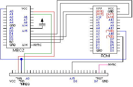


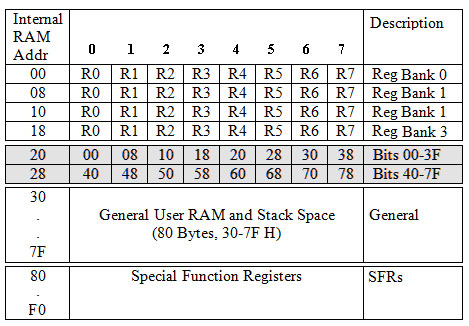


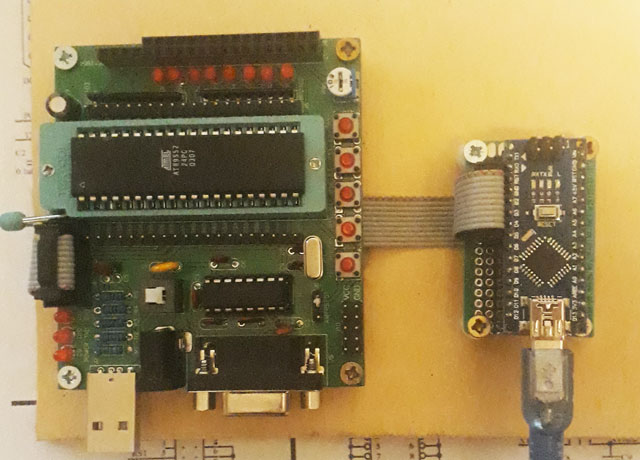


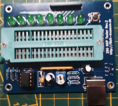
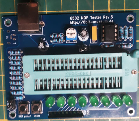

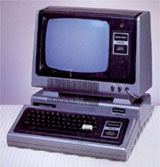


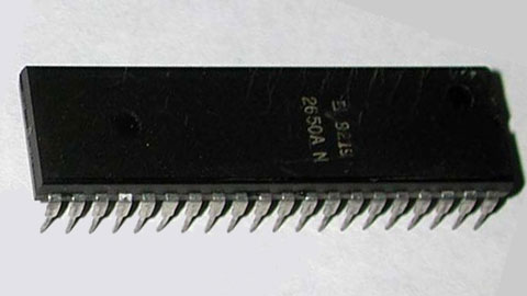


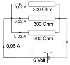


 Een potentiometer, ook wel potmeter genoemd, is een instelbare spanningsdeler, waarbij de verhouding tussen de twee weerstandswaarden en de midden aftakking tussen 0 en de maximale waarde ingesteld kan worden. Potentiometers zijn er in vele uitvoeringen, veel mensen kennen de potentiometer als draaiknop voor bijvoorbeeld de volumeregeling. Maar op mengpanelen zien we ook vaak de combinatie van draaipotmeters en langwerpige schuifpotmeters. Maar op printplaten zien we ook vaak de zogenaamde instelpotmeters die met een schroevendraaier ingesteld kunnen worden. Een potmeter bestaat meestal uit een rechte of ronde plaat met een weerstand baan waar een sleepcontact overheen loopt, die op deze wijze de weerstand baan in twee delen opsplitst. Zo ontstaat dus een weerstand aan weerszijden van de aftakking die kan veranderen door het sleepcontact te verplaatsen. Er bestaan ook stereo potmeters waarbij er twee weerstand banen aan één as of schuif gemonteerd zijn.


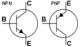


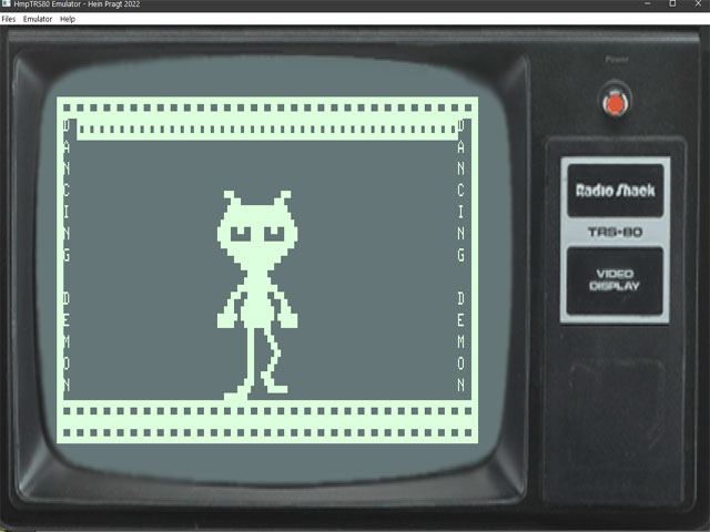


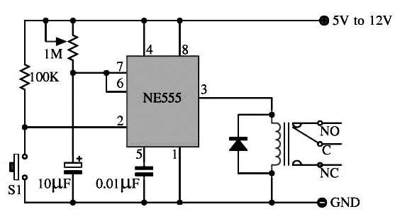


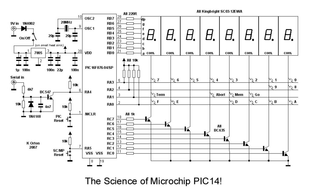
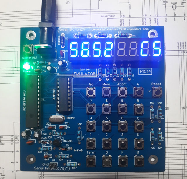

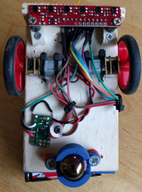


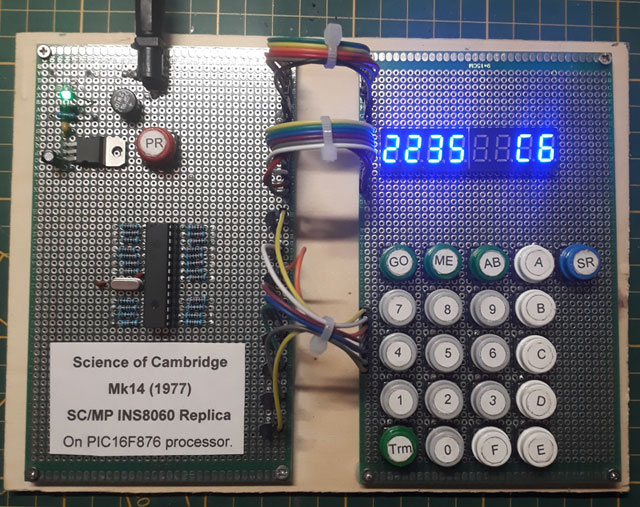


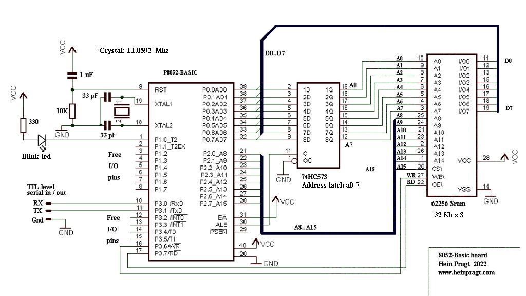


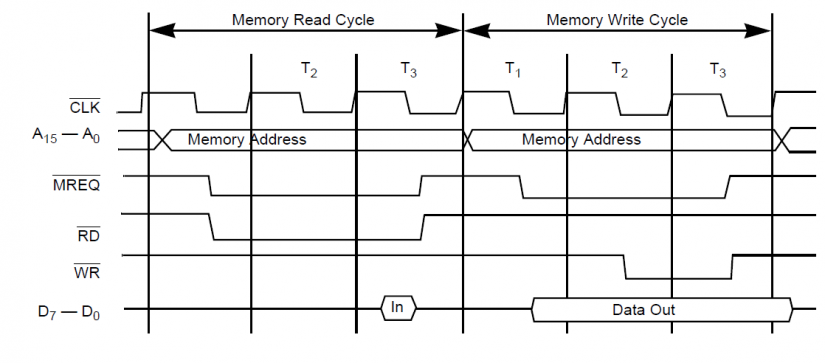
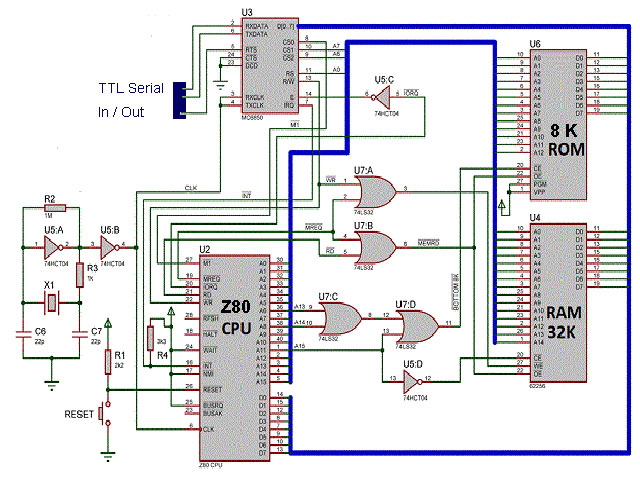


 As you can read on other pages, I am a reasonable fan of the Z80 processor. The Z80 is officially an 8 bit processor but also has registers that can be used as a pair as a 16 bit register. That’s why I was surprised to read that the Z80 actually has a 4-bit ALU (Arithmetic logic unit). How that works I try to explain on this page. The makers of the Z80 are already dropping something about this in a

